 Open Access Article
Creative Commons Attribution 3.0 Unported Licence
Low temperature fabrication of thermochromic VO2 thin films by low-pressure chemical vapor deposition
Beibei Guoa,
Lanli Chena,
Siqi Shi a,
Ahmad Ishaqb,
Dongyun Wan*a,
Zhang Chena,
Liangmiao Zhanga,
Hongjie Luoa and
Yanfeng Gao
 *a
*a
aSchool of Materials Science and Engineering, Shanghai University, Shanghai 200444, China. E-mail: echowandy@shu.edu.cn; yfgao@shu.edu.cn
bNational Center for Physics, Quaid-I-Azam University, Islamabad 44000, Pakistan
First published on 9th February 2017
Abstract
VO2(M) is of special interest as the material with the most potential for future application in smart windows and switching devices. However, a number of drawbacks need to be overcome, including the high processing temperature of current synthesis techniques and low thermochromic properties. This work reports the fabrication of high-performance thermochromic VO2 thin films at low temperatures below 400 °C based on a low-pressure chemical vapor deposition (LPCVD) with a vanadium(III) acetylacetonate precursor. Proper tuning of the process parameters is found to be critical in fabricating thickness-controllable highly-crystalline VO2 films. For an ∼62 nm thick VO2 film, visible transmittances of 52.3% (annealed at 400 °C) and 52.7% (annealed at 350 °C) were obtained. The corresponding solar energy modification abilities (ΔTsol) were 9.7% and 7.1%, and the transition temperatures were 45.1 °C and 50.9 °C. The underlying microscopic mechanism was studied by first-principles calculations and the results indicated that improved performances, including a low transition temperature, could be achieved by properly controlling the annealing temperature, ascribed to the combined effect of strain and oxygen vacancies. Moreover, the initial use of a pre-grown seed layer induced fast grain growth, which is favorable for further decreasing the deposition and annealing temperature to 325 °C.
1. Introduction
Vanadium dioxide (VO2), a kind of thermochromic material, exhibits a strong reversible thermal-induced metal-insulator phase transition (MIPT) at 68 °C,1–3 which is accompanied by a dramatic change in its optical properties.4 Based on the unique characteristics of VO2, thermochromic VO2 thin films can be used in smart windows5–7 and switching devices.8,9Various methods have been reported regarding the growth of VO2 thin films, such as sputtering,10,11 pulsed laser deposition,12 solution-based processing13–15 and chemical vapor deposition.5,16–21 Because of its high deposition rate, low-cost, large area growth and simplicity of doping, chemical vapor deposition (CVD) is a widely available and attractive method for the deposition of thin films. By altering parameters such as the deposition temperature, time, precursor species, vapor composition and flow rates, this method is capable of achieving a high degree of control over the morphology, crystallinity and properties of the VO2 thin films, hence obtaining highly crystallized, tough, and durable layers. The precursor species that have been utilized chiefly include VOCl3,16–18 VCl4,5,19,21 vanadium(IV) acetylacetonate (VO(acac)2),20,21 and vanadium(III) acetylacetonate (V(acac)3).20,22 These studies came to the conclusion that a high temperature advanced the growth of oxygen-deficient phases, and that the formation temperature of monoclinic VO2 should be kept above 450 °C (even up to 600 °C).5,16,19,20,22 However, as a prospective material for smart windows and switching devices, a high deposition temperature apparently limits the application of VO2 on the large arrays of integrated silicon circuits, and limits the choice of substrates to rigid ones. Therefore, research into low-temperature preparation processes is imperative.23,24
In this paper, pure monoclinic VO2 thin films were fabricated from directly available solid vanadium(III) acetylacetonate at 350–450 °C on quartz and silicon substrates by low-pressure chemical vapor deposition (LPCVD), using a multi-zone heating furnace. The as-prepared VO2 thin films exhibited relatively high crystallinity, porous morphology and excellent thermochromic performance, which will further prompt the practical application of VO2-based materials for smart windows. In addition, the combined nucleation/growth film deposition process was divided into two separate steps in our work; the seed layer produced in the first step could obstruct the further nucleation of new grains and promote the fast growth of existing grains during the second step,25 and the deposition and annealing temperature was effectively decreased to 325 °C. The feasibility of this method provides a new strategy for further reducing the deposition and annealing temperature simultaneously.
2. Experimental section
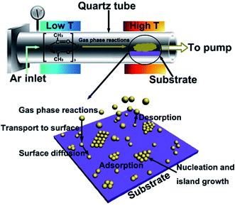
Vanadium(III) acetylacetonate (Sinopharm Chemical Reagent Co., Ltd, 97%) was employed as a precursor. The film fabrication included a CVD process and a post-annealing process, and therefore involved a deposition temperature and an annealing temperature. The deposition and annealing processes were carried out in a split vacuum/atmosphere tube furnace, which consists of a temperature controller, a reaction chamber, a vacuum & pressure controller and a gas flow controller. All of the experiments were performed in a high-purity argon (99.99%) atmosphere. Prior to deposition, the glass and silicon substrates were cleaned using deionized water, ammonia, hydrogen peroxide, acetone, and ethanol, and then blow-dried in air before use.A schematic representation of the LPCVD in a three-zone furnace and the CVD reaction process is shown in Fig. 1. The vanadium(III) acetylacetonate precursor was placed in a low temperature zone (blue areas situated at the left of the tube in Fig. 1) and the temperature was set at 150 °C. Meanwhile, the substrates were put into a high temperature zone (red areas situated at the right of the tube in Fig. 1) and the substrate temperature (deposition temperature) was set at 350 °C. The deposition time ranged from 30 to 120 min. Then the as-deposited samples were annealed at 300–450 °C for 2 h. A flow of argon was passed through the tube during the whole deposition and annealing process. The samples were removed from the furnace below 50 °C and stored in air.
In the two-step process, a thin seed layer was formed on the substrate in the first step at 300 °C for 2 h, followed by growth of an overlayer in the second step at 325 °C for 5.5 h. Then the samples were annealed at 325 °C for 8 h. For comparison, samples were also prepared using a one-step deposition at 325 °C for 6 h, and then treated under identical annealing conditions.
The crystallization and phase structures of the thin films were characterized by X-ray diffraction measurements (XRD, Model D/Max 2200 V, Rigaku). The morphology and the thickness of the films were measured using a scanning electron microscope (SEM, S4800, Hitachi), an atomic force microscope (AFM, Asylum Research), and a profilometer (Dektak 150, Veeco). X-ray photoelectron spectroscopy (XPS) experiments were carried out on an ESCA 2000 system (VG Microtech: UK) with twin anode Al Kα (1486.6 eV)/Mg Kα (1253.6 eV) X-ray sources to characterize the valence state of the elements and the stoichiometric change in the thin films. A Raman Renishaw RM3000 spectrometer was used to analyze the chemical bonding between the various elements and compounds. The optical transmittance characteristics were monitored on a Hitachi UH4150 UV-visible-near-IR spectrophotometer equipped with a controllable heating unit in the wavelength range of 300–2600 nm. The temperature between 20 °C and 90 °C was measured using a thermocouple in contact with the films, and was controlled using a temperature-control unit.
3. Results and discussion
3.1 Effect of the deposition time
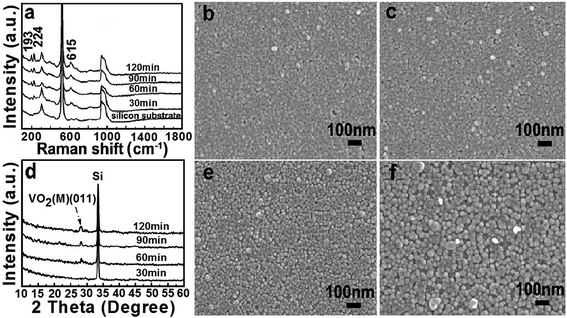
The film thickness is a key factor that affects the optical properties of the VO2 films. Consequently, the thickness was controlled and the optical properties were tuned by regulating the deposition time of the VO2 films in our work. Fig. 2 shows the Raman spectra, X-ray diffraction (XRD) patterns and SEM photographs of the films that were deposited at 350 °C for different deposition time, and then annealed at 350 °C for 2 h. In Fig. 2(a), the Raman modes centered at 193, 224 and 615 cm−1 are in agreement with the reported data of VO2(M). No other impurities, such as carbon contamination with Raman shifts at around 1360 and 1591 cm−1,26 are found. In addition, no changes in the phase composition occurred from 30 min to 120 min. The X-ray diffraction patterns of the films (Fig. 2(d)) can be readily indexed to VO2(M) (JCPDS card no. 43-1051), with peaks representing the (011) reflections, which is consistent with the Raman results. The thicknesses of the films are ∼31 nm (30 min), ∼53 nm (60 min), ∼62 nm (90 min) and ∼67 nm (120 min). The SEM photographs show that the four different films, with high surface coverage, consist of nanometer-sized, well-distributed particles. As the deposition time is prolonged from 30 to 90 min, as shown in Fig. 2(b), (c) and (e), the particle size increases indistinctly, and the mean diameter is around 15 nm. From 90 to 120 min, there is evident growth in the particle size (Fig. 2(e) and (f)). Furthermore, many nanosized defined pores appear in the films. This porous microstructure is favorable for improvement of the thermochromic optical properties of the VO2 films,15,27 which will be discussed in the next section.Extremely obvious transmittance differences were observed at 20 and 90 °C in Fig. 3(a). Table 1 contains the optical performance parameters of the films that were deposited at 350 °C for different deposition time, and then annealed at 350 °C for 2 h. Generally speaking, the luminous transmittance (Tlum) decreases and the solar energy modification ability (ΔTsol) rises as the thickness increases. There is a mutual restraint relationship between Tlum and ΔTsol. On the basis of the practical application requirements of smart windows, the optimum Tlum is about or above 50%, while the ΔTsol value should be as large as possible. The optical properties of the VO2(M) thin films that were deposited at 350 °C for 90 min and then annealed at 350 °C for 2 h are prominent (ΔTsol = 7.1% and Tlum = 52.7%.). Further extending the deposition time will substantially impair Tlum. Therefore, the conditions of depositing for 90 min at 350 °C and then annealing at 350 °C for 2 h are suitable for preparing high-performance thermochromic VO2(M) thin films.
| Deposition time (min) | Luminous transmittance, Tlum (%) | Solar transmittance, Tsol (%) | Solar energy modification ability, ΔTsol (%) | ||
|---|---|---|---|---|---|
| 20 °C | 90 °C | 20 °C | 90 °C | ||
| 30 | 70.9 | 71.5 | 72.8 | 69.4 | 3.3 |
| 60 | 52.8 | 55.3 | 57.8 | 52.6 | 5.3 |
| 90 | 52.7 | 53.9 | 56.6 | 49.6 | 7.1 |
| 120 | 48.7 | 49.8 | 52.5 | 45.7 | 6.9 |
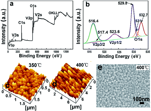
The hysteresis loops of the films that were deposited at 350 °C for different deposition time and then annealed at 350 °C for 2 h can be seen in Fig. 3(b), and were obtained by measuring the transmittance alteration at 2000 nm with continuous heating (solid lines) and cooling (dashed lines). Through the hysteresis loops, the MIPT temperatures were calculated. The correspondence between the deposition time and the MIPT temperature is listed in the top right corner of Fig. 3(b). The MIPT temperature, another vital thermochromic performance parameter, decreases as the thickness increases within a certain range, with the observed values being 56.0 °C (30 min), 52.2 °C (60 min), 50.9 °C (90 min) and 48.5 °C (120 min). There are many factors that can bring about an MIPT temperature below 68 °C, including oxygen vacancies, which can enhance the electron concentration and thus decrease the MIPT temperature. The O1s XPS spectrum of the VO2 thin film that was deposited at 350 °C for 90 min and then annealed at 350 °C for 2 h in Fig. 3(c) shows that several kinds of binding states coexist in the film. One of the peaks at 531 eV (530.7 eV,28 531.6 eV (ref. 29)) may be related to oxygen vacancies. Based on first principles calculations, our recent simulation results36 showed that the MIPT temperature steeply declines as a result of the formation of oxygen vacancies in films. Hence the decrease of the MIPT temperature of our CVD-prepared films compared with pure VO2(M) most likely originates from the existence of oxygen vacancies in the films.
3.2 Effect of the annealing temperature
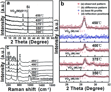
From the above results, it can be found that high-performance thermochromic VO2(M) thin films that were deposited at 350 °C for 90 min and then annealed at 350 °C for 2 h could be achieved. However, the annealing temperature has a great impact on the crystallinity and optical properties of the VO2 films. The XRD patterns, Rietveld refinement fitting results30 acquired using the Software Program TOPAS 4.1 and Raman spectra of the films that were deposited at 350 °C for 90 min and then annealed at different temperatures for 2 h are shown in Fig. 4(a–c), respectively. It can be seen from Fig. 4(a) and (c) that weak Raman peaks at 194 and 224 cm−1 and shifts for carbon (between 1200 and 1600 cm−1) exist within the film that was annealed at 300 °C, but there is no diffraction peak in the XRD diagram. Therefore, annealing the films at 300 °C or below is not conducive to crystallization. When the annealing temperature was above 350 °C, the shifts for carbon disappeared, and evident diffraction peaks and Raman modes basically centered at 143 (143 (ref. 5)), 194 (192,5 195 (ref. 31)), 224 (223,5 222 (ref. 31)), 259 (261 (ref. 5)), 389 (390 (ref. 5)), and 615 cm−1 (612,5 622 (ref. 31)) corresponding to VO2(M) are observed. Accordingly, in order to avoid the influences of other phases (e.g., carbon) and thus obtain pure VO2 films, the annealing temperature should be higher than 350 °C. Moreover, an increase in the peak intensity means an improvement in the crystallinity of the VO2 films as the annealing temperature increases. Therefore, a suitable annealing temperature is critical to obtain high-crystallinity pure VO2(M) films.XPS measurement of the film that was deposited at 350 °C for 90 min and annealed at 400 °C for 2 h was performed to clarify the detailed composition and to gain an insight into the oxidation states of the ions present. The wide range survey spectrum suggests the presence of vanadium, oxygen, and carbon, as shown in Fig. 5(a). The V2p core-level spectrum is composed of V2p3/2 and V2p1/2, which is attributed to the spin–orbit splitting of the components. The peaks at binding energies of 516.4 eV (reported values: 515.7–516.2,32–34 516.4 (ref. 28)) and 517.4 eV (reported values: 517.2,32 517.4 (ref. 28)) can be assigned to two different vanadium valence states, V4+ and V5+, respectively (Fig. 5(b)). A trace amount of V5+ is detected mostly on account of surface oxidization, either during the annealing process or during storage in air.34 The O1s spectrum can be deconvoluted into three peaks. One of the peaks at the binding energy of 529.8 eV (530.0 eV (ref. 35)) corresponds to oxygen bound to vanadium, while the peak at 531 eV is related to oxygen vacancies. Compared with Fig. 3(c), it is found that as the oxygen vacancy concentration in VO2 increases, the Tc decreases sharply, which has also been proved in our previous study from first principles calculations.36 The peak at 532.7 eV (532.6 eV (ref. 16)) is assigned to residual contamination of carbon-containing species or is due to OH (532.2 eV (ref. 37)) (Fig. 5(b)). The residual carbon contamination in the film is mainly due to the incomplete oxidation of the carbon element in the V(acac)3 precursor.
The surface morphology and microstructure were characterized by SEM and AFM, respectively. The top-view SEM and AFM images of the film that was annealed at 400 °C in Fig. 5(e) and (d) reveal that the film is homogeneous and consists of interconnected particles and irregular nanopores. The sizes of the particles are no larger than 100 nm. The grain sizes of the film are below the wavelength of visible and infrared light, which together with the porosity is beneficial for improving the optical quality.15,27 Fig. 5(c) is the AFM photograph of the film that was annealed at 350 °C. The root-mean-square (rms) roughness values of the two films are 31.87 (400 °C) and 6.31 nm (350 °C). The film with a rougher surface obtained by annealing at 400 °C showed better crystallinity than the film annealed at 350 °C.
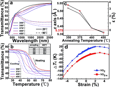
As seen in Fig. 6(a), there is almost no transmittance difference for the film that was annealed at 300 °C (black lines in Fig. 6(a), the solid and dashed lines are for the films that were measured at 20 °C and 90 °C, respectively). However, extremely remarkable transmittance differences were observed for the films that were annealed at 350–450 °C in the short-wave-near-infrared (780–2600 nm) region, which also indicates the generation of VO2(M). The optical performance parameters of the films that were annealed at different temperatures are listed in Table 2. A ΔTsol of 9.7% and a Tlum of 52.3% (20 °C) were achieved for the VO2(M) film that was annealed at 400 °C. These excellent thermochromic properties are comparable to the reported values for single layer VO2 films. Reported data shows that for single layer VO2 films, the ΔTsol is only 7.1% at Tlum = 50%, and increasing the film thickness could improve ΔTsol to 9.9%, but Tlum dropped to 12.5%.29
| Annealing temperature (°C) | Luminous transmittance, Tlum (%) | Solar transmittance, Tsol (%) | Solar energy modification ability, ΔTsol (%) | ||
|---|---|---|---|---|---|
| 20 °C | 90 °C | 20 °C | 90 °C | ||
| 350 | 52.7 | 53.9 | 56.6 | 49.6 | 7.1 |
| 375 | 52.6 | 52.1 | 58.0 | 49.5 | 8.5 |
| 400 | 52.3 | 50.9 | 58.6 | 48.8 | 9.7 |
| 450 | 49.6 | 51.2 | 59.3 | 50.9 | 8.5 |
Fig. 6(b) exhibits the hysteresis loops of the films that were annealed at different temperatures, which were obtained by measuring the transmittance alteration at 2000 nm with continuous heating (solid lines) and cooling (dashed lines). The correspondence between the annealing temperatures and the MIPT temperatures is listed in the top right corner of Fig. 6(b). The MIPT temperatures are 50.9 °C (350 °C), 48.0 °C (375 °C), 45.1 °C (400 °C) and 49.8 °C (450 °C). The hysteresis loop widths are 12.3 °C (350 °C) and 9.5 °C (400 °C). Compared with the typical MIPT temperature (68 °C) and hysteresis loop width (25.7 °C (ref. 13)) of VO2(M) films, the MIPT temperatures of the above films are lower and get increasingly closer to room temperature, particularly the minimum value of 45.1 °C (400 °C), which is crucial for application of this material in smart windows. Apart from this, the hysteresis loop widths are plainly narrowed. These results may be related to the nanoscale grain size, which contributes to reducing the MIPT temperature and narrowing the hysteresis loops (a grain size of 3.2 nm corresponds to a hysteresis width of 19.5 °C (ref. 38)). Meanwhile, the MIPT temperature firstly falls and then rises as the annealing temperature is increased, and this trend is probably due to the combined effect of strain and oxygen vacancies.
Fig. 6(c) shows the variation of the c axis of the VO2(M) films with increasing annealing temperature, with the lattice parameters acquired from the fitting results in Fig. 4(b). Here, the strain can be defined as ε = (c − c0)/c0, where c0 (c0 = 5.375 Å) and c are the supercell lengths along the c axis under equilibrium conditions and strain, respectively. The solid stars correspond to the left y-axis and the hollow stars refer to the right y-axis. The strain values are 3.1% (350 °C), 2.3% (375 °C), 0.3% (400 °C) and −0.3% (450 °C). ε > 0 signifies tension, while the opposite indicates compression. It can be observed in Fig. 6(c) that the tension gradually decreases and becomes compressive strain with the increase of annealing temperature.
First principles calculations were performed in a supercell with a 2 × 2 × 2 primitive unit cell for VO2(M) consisting of 96 atoms (excluding oxygen vacancies). The ratio between the oxygen vacancies and oxygen atoms in the supercell is about 1.56%, which has been discussed in our previous study.36 The MIPT temperature (Tc) can be quantitatively calculated via39
 | (1) |
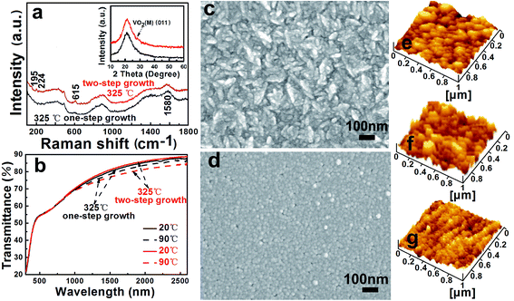
3.3 Two-step growth process
To further reduce the deposition and annealing temperature, a novel two-step growth process was employed in our experiment. Raman spectra (a), X-ray diffraction patterns (inset in (a)) and transmittance spectra (b) of the films that were prepared concurrently by one-step deposition (black lines) and two-step deposition (red lines) can be seen in Fig. 7. The results in Fig. 7(a) show no distinctive Raman and XRD diffraction peaks for the thin film that was prepared by one-step deposition, even upon extending the deposition and annealing time while further dropping the temperature to 325 °C. The transmittance–wavelength curves at high and low temperatures reveal that there is almost no phase transition. On the contrary, the film that was fabricated using a two-step deposition process showed distinguishable diffraction and Raman peaks, although the crystallinity remains poor. There is also a more evident transmittance difference at 20 and 90 °C for the film that was prepared by two-step deposition (red line in Fig. 7(b)). A large number of crystal nuclei form in the seed layer during the first deposition step, which can be regarded as the seeds of the overlayer. The overlayer then grows rapidly along the direction of the crystal lattice of the seed layer directly without nucleation during the annealing process. Therefore, the assistance of the seed layer can allow crystallized VO2 thin films to be obtained even if the deposition and annealing temperature is as low as 325 °C.Fig. 7(c) and (d) show SEM images of the films that were prepared by one-step deposition (without a seed layer) and two-step deposition (with a seed layer), respectively. By comparing the two images, it can be seen that the grain sizes of the film that was prepared without a seed layer are uneven and significant clustering can be observed. On the contrary, the grain sizes of the film that was prepared with a seed layer are fine, and uniform particles with no distinct clustering can be seen. The latter result may be attributed to the competition effect among the adjacent crystal nuclei, which restricts the space for growth during the annealing process. Nevertheless, only a small number of crystal nuclei initially form in the film that was prepared without a seed layer, which can grow into large grains, whereas the new crystal nuclei are subsequently limited to growing in the interspaces between the large grains. Thus, the newly formed grains are small, and have a large specific surface area that makes them prone to adsorbing onto the large grains resulting in clusters. The root-mean-square (rms) roughness values of the films are 2.50, 4.43 nm and 0.40 nm (from the AFM images seen in Fig. 7(e), (f) and (g) for the films that were prepared by one-step deposition (without a seed layer), two-step deposition (with a seed layer) and the seed layer, respectively). Thus the film with a seed layer is a better-crystallized VO2 film with a rougher surface than that without a seed layer.
4. Conclusions
In this paper, monoclinic VO2 thin films have been successfully prepared using a vanadium(III) acetylacetonate precursor at 350–450 °C, and subsequently at a lower temperature of 325 °C by low-pressure chemical vapor deposition (LPCVD). The process parameters, such as deposition time and annealing temperature, are critical to obtain thickness-controllable nanoporous high-performance VO2(M) thin films. The VO2(M) thin films that were annealed at 400 °C display outstanding thermochromic properties, which are suitable for smart window applications. Although the properties of the VO2(M) thin films that were annealed at 350 °C are comparatively poorer, their low temperature fabrication gives them fairly strong practical value. The underlying causes of the noticeable decrease in MIPT temperature for our CVD-prepared films compared with pure VO2(M) films, and the connection between the annealing temperature and the MIPT temperature were studied using first principles calculations. The results indicated that the annealing temperature and the strain in the films are directly related, while the combined effect of strain and oxygen vacancies together determine the MIPT temperature of VO2. In addition, a two-step deposition method is found to be facile and has great potential for the fabrication and development of VO2(M) thin films, accordingly reducing the deposition and annealing temperature simultaneously, which is favorable for application in flexible films.Acknowledgements
This work is supported by the joint foundation of the National Natural Science Foundation of China and the Big Science Facility of the Chinese Academy of Sciences (No. U1632108), the National Natural Science Foundation of China (No. 51622207 and U1630134), and funding from the Ministry of Science and Technology of China (2016YFB0303901-05). Gao acknowledges funding from the State Outstanding Young Scholars (51325203) and Changjiang Scholars programs.References
- J. B. Goodenough, J. Solid State Chem., 1971, 3, 490–500 CrossRef CAS.
- T. D. Manning, I. P. Parkin, C. Blackman and U. Qureshi, J. Mater. Chem., 2005, 15, 4560–4566 RSC.
- F. J. Morin, Phys. Rev. Lett., 1959, 3, 34–36 CrossRef CAS.
- Z. Chen, Y. F. Gao, L. T. Kang, C. X. Cao, S. Chen and H. J. Luo, J. Mater. Chem. A, 2014, 2, 2718–2727 CAS.
- T. D. Manning, I. P. Parkin, R. J. H. Clark, D. Sheel, M. E. Pemble and D. Vernadou, J. Mater. Chem., 2002, 12, 2936–2939 RSC.
- M. Kamalisarvestani, R. Saidur, S. Mekhilef and F. S. Javadi, Renewable Sustainable Energy Rev., 2013, 26, 353–364 CrossRef CAS.
- Y. F. Gao, S. B. Wang, L. T. Kang, Z. Chen, J. Du, X. L. Liu, H. J. Luo and M. Kanehira, Energy Environ. Sci., 2012, 5, 8234–8237 CAS.
- G. Seo, B. J. Kim, H. T. Kim and Y. W. Lee, Curr. Appl. Phys., 2014, 14, 1251–1256 CrossRef.
- A. Velichko, A. Pergament, V. Putrolaynen, O. Berezina and G. Stefanovich, Mater. Sci. Semicond. Process., 2015, 29, 315–320 CrossRef CAS.
- N. Y. Shishkin, A. A. Komarov, D. V. Kosov, V. A. Cherkasov, L. A. Bashkirov, U. Bardi and Y. K. Gunko, Sens. Actuators, B, 2005, 108, 113–118 CrossRef CAS.
- J. O. Choi, H. S. Lee and K. H. Ko, J. Mater. Sci., 2014, 49, 5087–5092 CrossRef CAS.
- T. H. Yang, S. Nori, H. H. Zhou and J. Narayan, Appl. Phys. Lett., 2009, 95, 102506 CrossRef.
- Z. T. Zhang, Y. F. Gao, H. J. Luo, L. T. Kang, Z. Chen, J. Du, M. Kanehira, Y. Z. Zhang and Z. L. Wang, Energy Environ. Sci., 2011, 4, 4290–4297 CAS.
- Z. T. Zhang, Y. F. Gao, Z. Chen, J. Du, C. X. Cao, L. T. Kang and H. J. Luo, Langmuir, 2010, 26, 10738–10744 CrossRef CAS PubMed.
- L. T. Kang, Y. F. Gao, H. J. Luo, Z. Chen, J. Du and Z. T. Zhang, ACS Appl. Mater. Interfaces, 2011, 3, 135–138 CAS.
- T. D. Manning and I. P. Parkin, Polyhedron, 2004, 23, 3087–3095 CrossRef CAS.
- U. Qureshi, T. D. Manning, C. Blackman and I. P. Parkin, Polyhedron, 2006, 25, 334–338 CrossRef CAS.
- U. Qureshi, T. D. Manning and I. P. Parkin, J. Mater. Chem., 2004, 14, 1190–1194 RSC.
- D. Vernardou, P. Paterakis, H. Drosos, E. Spanakis, I. M. Povey, M. E. Pemble, E. Koudoumas and N. Katsarakis, Sol. Energy Mater. Sol. Cells, 2011, 95, 2842–2847 CrossRef CAS.
- C. Piccirillo, R. Binions and I. P. Parkin, Chem. Vap. Deposition, 2007, 13, 145–151 CrossRef CAS.
- D. Vernardou, M. E. Pemble and D. W. Sheel, Chem. Vap. Deposition, 2006, 12, 263–274 CrossRef CAS.
- T. Maruyama and Y. Ikuta, J. Mater. Sci., 1993, 28, 5073–5078 CrossRef CAS.
- H. Kim, Y. Kim, K. S. Kim, H. Y. Jeong, A. R. Jang, S. H. Han, D. H. Yoon, K. S. Suh, H. S. Shin, T. Y. Kim and W. S. Yang, ACS Nano, 2013, 7, 5769–5776 CrossRef CAS PubMed.
- A. H. Fang, F. Q. Huang, X. M. Xie and M. H. Jiang, J. Am. Chem. Soc., 2010, 132, 3260–3261 CrossRef CAS PubMed.
- D. Y. Wan, F. Q. Huang and Y. M. Wang, ACS Appl. Mater. Interfaces, 2010, 2, 2147–2152 CAS.
- V. G. Pol, S. V. Pol, J. M. Calderon-Moreno and A. Gedanken, J. Phys. Chem. C, 2009, 113, 10500–10504 CAS.
- P. Jin, Japanese patent 2007171759-A, 2007.
- H. Q. Zhao, J. O. Wang, L. X. Zhang, Y. C. Rong, J. Chen, K. Ibrahim and X. R. Xing, Dalton Trans., 2013, 42, 10358–10364 RSC.
- J. Y. Gan, X. H. Lu, J. H. Wu, S. L. Xie, T. Zhai, M. H. Yu, Z. S. Zhang, Y. C. Mao, S. C. I. Wang, Y. Shen and Y. X. Tong, Sci. Rep., 2013, 3, 1021 Search PubMed.
- V. Melnik, I. Khatsevych, V. Kladko, A. Kuchuk, V. Nikirin and B. Romanyuk, Mater. Lett., 2012, 68, 215–217 CrossRef CAS.
- H. T. Kim, B. G. Chae, D. H. Youn, G. Kim, K. Y. Kang, S. J. Lee, K. Kim and Y. S. Lim, Appl. Phys. Lett., 2005, 86, 242101 CrossRef.
- N. Alov, D. Kutsko, I. Spirovova and Z. Bastl, Surf. Sci., 2006, 600, 1628–1631 CrossRef CAS.
- R. Lindstrom, V. Maurice, S. Zanna, L. Klein, H. Groult, L. Perrigaud, C. Cohen and P. Marcus, Surf. Interface Anal., 2006, 38, 6–18 CrossRef CAS.
- C. C. Hu, H. H. Xu, X. X. Liu, F. Zou, L. Qie, Y. H. Huang and X. L. Hu, Sci. Rep., 2015, 5, 16012 CrossRef PubMed.
- G. Silversmit, D. Depla, H. Poelman, G. B. Marin and R. D. Gryse, J. Electron Spectrosc. Relat. Phenom., 2004, 135, 167–175 CrossRef CAS.
- L. Chen, X. Wang, D. Wang, Y. Cui, B. Liu, S. Shi, H. Luo and Y. Gao, RSC Adv., 2016, 6, 73070–73082 RSC.
- M. Sathiya, A. S. Prakash, K. Ramesha, J. M. Tarascon and A. K. Shukla, J. Am. Chem. Soc., 2011, 133, 16291–16299 CrossRef CAS PubMed.
- L. Dai, C. X. Cao, Y. F. Gao and H. J. Luo, Sol. Energy Mater. Sol. Cells, 2011, 95, 712–715 CrossRef CAS.
- M. Netsianda, P. E. Ngoepe, C. Richard, A. Catlow and S. M. Woodley, Chem. Mater., 2008, 20, 1764–1772 CrossRef CAS.
| This journal is © The Royal Society of Chemistry 2017 |

