 Open Access Article
Creative Commons Attribution 3.0 Unported Licence
Generation of 3-dimensional polymer structures in liquid crystalline devices using direct laser writing†
C. C.
Tartan
*a,
P. S.
Salter
a,
T. D.
Wilkinson
b,
M. J.
Booth
a,
S. M.
Morris
a and
S. J.
Elston
*a
aDepartment of Engineering Science, University of Oxford, Parks Road, Oxford, OX1 3PJ, UK. E-mail: steve.elston@eng.ox.ac.uk; chloe.tartan@eng.ox.ac.uk
bDepartment of Engineering, University of Cambridge, 9 JJ Thomson Avenue, Cambridge, CB3 0FA, UK
First published on 3rd January 2017
Abstract
Direct laser writing is a powerful nonlinear fabrication technique that provides high intensities in the focal plane of a sample to engineer multidimensional structures with submicron feature sizes. Dielectrically and optically anisotropic soft matter is of particular interest when considering a host medium in which exotic topological characteristics may be generated. In this manuscript, we adopt a novel approach for direct laser writing of polymeric structures, whereby the photo-sensitive resin is liquid crystalline (LC) and aligned within electrically addressable LC devices. We show that the laser written polymer structures retain the optical properties of the liquid crystal resin at the point of laser exposure. Thus, birefringent polymer structures can be written, with the orientation of the optic axis tuned during fabrication through switching the liquid crystal with an applied electric field. This gives the potential to create complex spatial variations of the polymer refractive index on a micron scale. Furthermore, we present a range of structures for controlling the liquid crystal alignment in devices, including two-dimensional arrays of polymer pillars, a polymer checkerboard that creates a controllable disclination network, and 3-dimensional helical polymer ribbons and knots. This work introduces a new degree of freedom for the direct laser writing of advanced photonic materials as well as offering significant advances for the control of soft matter.
Introduction
Direct laser writing (DLW) involving two-photon polymerization (TPP) is a nonlinear optical process that enables polymer structures to be fabricated with sub-micron feature sizes.1 The TPP process permits the fabrication of structures with three dimensional resolution that would not otherwise be attainable using conventional single photon laser fabrication techniques.2–4 An important application of TPP is the fabrication of photonic materials, and to this end three dimensional polymer scaffolds manufactured by DLW have subsequently been further functionalized by infusion with liquid crystalline (LC) materials to give dynamic tuning of the optical properties.5–10 More recently, it has been shown that DLW can also be used to fabricate elastomeric materials directly inside the LC host.11,12Despite these notable achievements, there have not been any reports dedicated to the fabrication of polymer structures directly into a fully assembled device where, crucially, the LC can be electrically addressed during laser writing so as to create a complex spatial variation of the refractive index on a micron scale. The main reason for this is that the relatively thick bounding glass substrates that contain transparent conductive coatings are some orders of magnitude thicker than the LC layer, and introduce strong spherical aberrations that lead to an enlarged focal spot and decrease in efficiency. Consequently, this then restricts the minimum size of the structures that can be directly fabricated into an LC device and, furthermore, conventional DLW systems are unable to fully exploit the electro-optic response of the LC at the time of fabrication.
Adaptive optics has in recent years been successfully applied to aberration correction in microscopy as well as DLW.13–15 In this paper, we show how a DLW fabrication system that incorporates adaptive optics aberration correction can be used to generate a variety of 2- and 3-dimensional polymer structures directly into an electrically addressed LC device. Here, polymeric structures are realised that exploit the switching properties of the LC molecules during photo-polymerization, i.e. at the moment of exposure to the laser beam. The polymer network locks-in the instantaneous alignment of the electrically-addressed LC molecules thus retaining its optical properties, such that polymer features with continuously tuneable birefringence can be created at a micron scale. This opens the door to a range of potential novel structures that are not realisable using conventional alignment techniques.
Experimental
Materials and sample preparation
The photo-polymerizable mixture used in this investigation consisted of 69 wt% of the nematic LC host, E7 (Merck Chemicals, Ltd), 30 wt% of the reactive mesogen RM257 (Merck Chemicals, Ltd) and 1 wt% of the photoinitiator IRG819 (Merck Chemicals, Ltd). The LC host material was chosen as it exhibits a nematic phase at room temperature and it has a positive dielectric anisotropy such that the LC molecules align along the direction of an applied electric field. The nematic LC host has a birefringence of Δn = 0.219 at λ = 632.8 nm and a dielectric anisotropy of Δε = 13.7 at a temperature of T = 20 °C. Throughout the investigation, each cell was capillary-filled when the photosensitive mixture was in the isotropic phase by mounting each cell on a hot plate set at T = 80 °C. The devices were then allowed to cool to room temperature before laser writing was initiated.Direct laser writing system
Ultrafast laser pulses from a titanium sapphire oscillator emitting 100 fs pulses at λ = 790 nm is focused using a high numerical aperture (NA) objective lens into the photosensitive LC sample for the development of the polymer network at the focal spot of the laser. The laser operates at a maximum power of 300 mW with a pulse repetition rate of 80 MHz. A 20× Zeiss objective lens with a 0.5 NA was used throughout the investigation, unless otherwise stated. A phase only LC spatial light modulator (Hamamatsu X10468-02) was imaged onto the pupil plane of the objective for aberration correction. The devices were mounted on a high precision air bearing translation stage and moved relative to the focus of the laser beam during fabrication. A more detailed explanation of the experimental apparatus can be found in ref. 16.Results and discussion
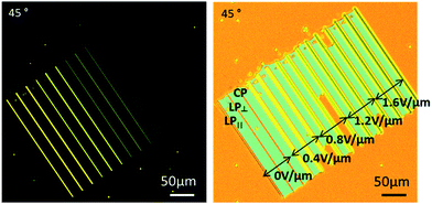
To begin with, we show polymer structures that lock-in the different birefringences associated with different LC alignments. In this case, a series of polymer walls were written into a 5 μm-thick, planar (parallel rubbed) nematic pi-cell device filled with the LC – monomer mixture under a range of applied electric field strengths. The walls were formed by translating the device through the laser focus at a speed of 25 μm s−1 and under continuous exposure to the femtosecond pulsed laser beam with an average power of Pav = 30 mW. A set of three walls were fabricated at each electric field strength with the writing laser beam being either circularly (CP) or linearly polarized (parallel (LP∥) and perpendicular (LP⊥) to the fabrication direction), to investigate whether any optical realignment of the LC director takes place during the polymerisation process. The microscope image on the left of Fig. 1 was taken when the device was heated to the isotropic phase at T = 80 °C. Evidently, the walls remain visible between crossed polarizers, revealing that the polymer structures display a degree of birefringence that changes according to the amplitude of the electric field that was applied to the device during laser writing. Moreover, these field-dependent LC states are recovered upon subsequent cooling to room temperature, as seen in the microscope image on the right of Fig. 1. The results in Fig. 1 show that walls fabricated with different polarizations of light are indistinguishable from one another. This confirms that the amplitude of the electric field of the laser is not large enough so as to distort the LC alignment during fabrication, but rather captures the director profile at the moment of exposure to the laser beam.In terms of more advanced photonic materials, two-dimensional square and hexagonal lattices of polymer pillars were engineered in a 20 μm-thick nematic pi-cell LC device. Arrays of pillars have previously been created in photoresists that are subsequently treated so as to induce certain alignments of the LC director post-fabrication. Such structures have been developed for the generation of bi-stable states in displays, or by epitaxial assembly for the formation of more complex LC phases.17,18 However, in these cases it was not possible to exploit the different director profiles that occur within an LC device under different applied electric field strengths. In this example, we have fabricated both square and hexagonal arrays of polymer pillars. The size and spacing of these pillars were controlled by the size of the focal spot of the laser and the diffusion properties of the polymer network. Here the pillars were written sequentially, with one pillar corresponding to one exposure of the ultra-fast laser.
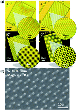
Fig. 2(a) presents microscope images of square and hexagonal arrays in their dark and bright states at two different device orientations (0° and 45° to the crossed polarizers, respectively). The polymer pillars were fabricated in situ under the application of a 0.4 V μm−1 electric field, where the molecules align in a bend configuration as illustrated in Fig. S1(b).† In this case, the pillars are expected to lock-in a hybrid (planar to homeotropic) director profile, while the remaining regions are able to switch freely when subjected to different electric field strengths due to the absence of a polymer network. The Scanning Electron Microscope (SEM) image in Fig. 2(b) of the hexagonal shaped pillar arrays shows the dimensions of the pillars to be ∼1.5 μm in diameter and ∼5 μm in height.
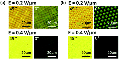
Fig. 3(a) and (b) are images of the dark and bright states for two different electric field amplitudes (see Fig. S1(d) and (e)† for additional field strengths). For most amplitudes, the alignment in and around the pillars is clearly distinguishable from the surrounding regions of the device: the one exception being when the same electric field as that used during fabrication is applied to the LC device. In this case, when the LC device is subjected to an electric field of E = 0.4 V μm−1, the director alignment within the region defined by the pillars was the same as that observed for the surrounding regions, indicating that the polymer pillars had indeed frozen-in the director profile of the LC that was present during fabrication.
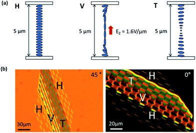
By applying an electric field during the laser writing process, it is also possible to create networks of disclinations directly within the LC device. Fig. 4 shows a checkerboard-type polymer structure that has been fabricated consisting of periodic walls that locked-in topologically distinct LC states. The device was a 5 μm thick, nematic pi-cell which undergoes a disclination mediated transformation from the equilibrium H state to the V state under an applied electric field, as sketched in Fig. 4(a), which then relaxes to the T state when the field is removed. The polymer walls, which extended through the bulk of the device from one substrate to the other, were written while the device existed in each of these 3 states: specifically, the walls are 10 μm in length and spaced at 5 μm intervals. The resultant checkerboard-type structure can be seen in Fig. 4(b) in the absence of an applied electric field during image capture. The region of the structure labelled ‘H’ is continuous with the bulk alignment around the checkerboard pattern as it was written in the absence of an electric field and so there is no discernible difference between the region defined by the checkerboard and the surrounding region.
The second region that was fabricated, labelled ‘V’ was written under an E = 1.6 V μm−1 electric field, which was sufficiently large to ensure that the entire device had been driven into the V (bend) state such that the polymer network then captured that alignment during the fabrication process.
Alternatively, upon removal of the applied field, it is known that the bend state collapses to a transient twisted alignment (T) state.19–21 Therefore, to capture and freeze-in the transient T state, the polymer network was formed before the device relaxed back to the ground (H) state. A final set of walls were then written once the device had returned to the H state (see Fig. 4(b)). Overall, the checkerboard pattern, therefore, consists of a series of polymer walls that were written at different electric field strengths, thereby locking-in topologically distinct director profiles, with a disclination loop separating the different regions. The close proximity of the polymer walls allows for the controllable introduction of disclination networks into an LC device.
Fig. 5 presents a sequence of images captured post-fabrication as the device is addressed with an increasing electric field. As the electric field strength is increased, the bend state grows out of the polymer structures that were fabricated either in the bend (field on – V) or twisted (removal of field – T) states, as these are energetically compatible due to their topological continuity. Upon removal of the electric field (t = 0 s), regions of the V state (bulk device) are found to collapse into the transient T state, which can be seen from the continuity between the bulk nematic LC and the region that consists of polymer network that has locked-in the bend and twisted alignments (see Fig. S2†). A domain wall forms around the topologically discontinuous line array that has locked-in the H state. Over time, the H state emanates from these structures written in the absence of an electric field (i.e. that have locked-in the H state) until the entire bulk relaxes to this lowest energy ground state.
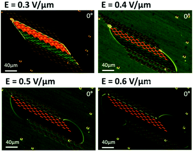 | ||
| Fig. 5 A series of microscope images showing the checkerboard-type structure in its dark state between crossed polarizers under varying electric field strengths. | ||
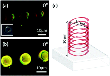
Finally, we provide examples of 3-dimensional polymer structures that have been written into our LC devices with and without the presence of an electric field. Initially, we fabricated 3-dimensional helical polymer ribbons into a 20 μm-thick, nematic Fréedericksz LC device that was filled with the same LC – monomer mixture used previously. The device was fabricated with a thin glass coverslip acting as the top substrate, permitting the use of a higher numerical aperture objective (1.4 NA oil immersion lens) which gives a greater resolution (∼1.2 μm) in the axial direction. The helical structures, 10 μm in diameter, shown in the microscope images of Fig. 6(a) and (b) were written whilst dynamically switching the electric field through the bulk and under continuous application of the field, respectively. The difference in birefringence between the helical polymer ribbons in Fig. 6(a) and (b) indicate that different alignments are indeed locked-in when the electric field is applied in situ. In this example, the polymer helices extend through the bulk of the device from one glass substrate to the other, as illustrated in Fig. 6(c).
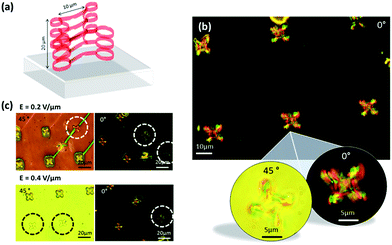
In addition to the helical ribbons, we have fabricated 3D polymer knots in the presence of an E = 0.4 V μm−1 electric field Fig. 7(a) is provided to aid in visualising the structure, which is shown in the microscope images of Fig. 7(b). Similar to the ribbons, these knots also extend through the bulk of the device. Previously, work has been carried out on the fabrication of complex topological structures, such as knots in colloidal systems in order to investigate self-assembled superstructures of knotted particles and defect networks with nanoparticles, but in this case there was no control of the alignment of the LC using an in situ electric field.22,23 The enlarged microscope images demonstrate how the transmission through the knot varies when the device is rotated between crossed polarizers, marking a clear distinction between the bright and dark optical states. The illustration in the electro-optic properties of the LC devices containing the polymer knots can be seen in Fig. 6(e) for two different applied electric field strengths, oriented in the bright and dark states of the device. The knots that have been circled in each image were written at the same electric field strength (i.e. E = 0.2 V μm−1 and E = 0.4 V μm−1) as that used to address the LC device when the images were captured after the fabrication process. When imaged using the corresponding field strength, it is clearly shown that the alignment of the LC appears continuous between the encircled polymer structures and the surrounding regions, for the remaining polymer structures, which were written at a different electric field strength to that used in the capture of the image, there is a clear distinction in the alignment between the region defined by the knots and the surrounding nematic LC. This confirms that the complex 3D polymer network has locked-in different director profiles depending upon the electric field amplitude that was applied during fabrication.
Conclusions
In conclusion, we have demonstrated the fabrication of complex, multi-dimensional micron-scale polymer structures with a tuneable birefringence under the application of an electric field. Specifically, our DLW system incorporates aberration correction to restore the diffraction-limited focus at the sample. This permits in situ fabrication, whereby polymeric structures can be engineered in to a photo-polymerizable LC sample whilst simultaneously electrically addressing the device so as to access the different director profiles. We have presented an array of different fabricated structures, including two-dimensional arrays of polymer pillars, a polymer checkerboard that locks-in topologically distinct states to create a controllable disclination network, and 3-dimensional helical polymer ribbons and knots. Collectively, these findings demonstrate the ability to create a complex spatial variation in the birefringence directly within an LC device that is on the micron-scale, opening up many new avenues in both soft matter physics and the DLW of photonic materials.Acknowledgements
The authors gratefully thank the Engineering and Physical Sciences Research Council (UK), Merck Chemicals Ltd, the Leverhulme Trust and The Royal Society for financial support.Notes and references
- S. Kawata, H.-B. Sun, T. Tanaka and K. Takada, Nature, 2001, 412, 697 CrossRef CAS PubMed.
- J. Hohmann, M. Renner, E. Waller and G. von Freymann, Adv. Opt. Mater., 2015, 3, 1488 CrossRef CAS.
- M. Farsari and B. N. Chichkov, Nat. Photonics, 2009, 3, 450 CrossRef CAS.
- M. Malinauskas, M. Farsari, A. Piskarskas and S. Juodkazis, Phys. Rep., 2013, 533, 1–31 CrossRef CAS.
- C.-H. Ho, Y.-C. Cheng, L. Maigyte, H. Zeng, J. Trull, C. Cojocaru and D. Wiersma, Appl. Phys. Lett., 2015, 106, 021113 CrossRef.
- C. Jisha, K.-C. Hsu, Y. Lin, J.-H. Lin, C.-C. Jeng and R.-K. Lee, CLEO-PR, 2013 Search PubMed.
- D. McPhail, M. Straub and M. Gu, Appl. Phys. Lett., 2005, 87, 091117 CrossRef.
- F. Serra, S. Eaton, R. Cerbino, M. Buscaglia, G. Cerullo, R. Osellame and T. Bellini, Adv. Funct. Mater., 2013, 23, 3990 CrossRef CAS.
- Z. Ji, X. Zhang, B. Shi, W. Li, W. Luo, I. Drevensek-Olenik, Q. Wu and J. Xu, Opt. Lett., 2016, 41, 336 CrossRef PubMed.
- T.-P. Kao, K.-C. Hsu, C.-H. Hung, C.-Y. Tai and C.-C. Sun, OECC2010, 2010 Search PubMed.
- H. Zeng, D. Martella, P. Wasylczyk, G. Cerretti, J.-C. Gomez Lavocat, C.-H. Ho, C. Parmeggiani and D. Wiersma, Adv. Mater., 2014, 26, 2319 CrossRef CAS PubMed.
- H. Zeng, P. Wasylczyk, G. Cerretti, D. Martella, C. Parmeggiani and D. Wiersma, Appl. Phys. Lett., 2015, 106, 111902 Search PubMed.
- M. Booth, Philos. Trans. R. Soc., A, 2007, 365, 2829 CrossRef PubMed.
- P. Salter and M. Booth, Opt. Express, 2012, 20, 19978 CrossRef CAS PubMed.
- P. Salter, A. Jesacher, J. Spring, B. Metcalf, N. Thomas-Peter, R. Simmonds, N. Langford, I. Walmsley and M. Booth, Opt. Lett., 2012, 37, 470 CrossRef CAS PubMed.
- C. Tartan, P. Salter, M. Booth, S. Morris and S. Elston, J. Appl. Phys., 2016, 119, 183106 CrossRef.
- A. Honglawan, D. Beller, M. Cavallaro, R. Kamien, K. Stebe and S. Yang, Adv. Mater., 2011, 23, 5519 CrossRef CAS PubMed.
- S. Kitson and A. Geisow, Appl. Phys. Lett., 2002, 80, 3635 CrossRef CAS.
- P. Brimicombe and E. Raynes, Liq. Cryst., 2005, 32, 1273 CrossRef CAS.
- P. Brimicombe and E. Raynes, Appl. Phys. Lett., 2006, 89, 031121 CrossRef.
- P. Bos and K. Koehler/Beran, Mol. Cryst. Liq. Cryst., 1984, 113, 329 CrossRef CAS.
- B. Senyuk, Q. Liu, S. He, R. Kamien, T. Lubensky and I. Smalyukh, Nature, 2013, 493, 200 CrossRef CAS PubMed.
- A. Martinez, M. Ravnik, B. Lucero, R. Visvanathan, S. Zumer and I. Smalyukh, Nat. Mater., 2014, 13, 258 CrossRef CAS PubMed.
Footnote |
| † Electronic supplementary information (ESI) available. See DOI: 10.1039/c6ra25091b |
| This journal is © The Royal Society of Chemistry 2017 |

