 Open Access Article
Creative Commons Attribution 3.0 Unported Licence
The novel and facile preparation of multilayer MoS2 crystals by a chelation-assisted sol–gel method and their electrochemical performance
Xingzhong Guo *,
Zichen Wang,
Wenjun Zhu and
Hui Yang*
School of Materials Science and Engineering, Zhejiang University, Xihu District, Hangzhou, 310027, China. E-mail: msewj01@zju.edu.cn; yanghui@zju.edu.cn; Fax: +86-571-8795-3054; Tel: +86-571-87953313 Tel: +86-571-8795-1408
First published on 30th January 2017
Abstract
Multilayer molybdenum disulfide (MoS2) was facilely prepared by a chelation-assisted sol–gel method with ammonium molybdate tetrahydrate ((NH4)6Mo7O24·4H2O) as the molybdenum source, thioacetamide (CH3CSNH2) as the sulfur source and diethylenetriamine pentaacetic acid (Dtpa) as the chelating agent, subsequently followed by high-temperature calcination. The chelating agent Dtpa ingeniously mediated the chelation reaction of the system and promoted the formation of a monolithic gel. The hexagonal MoS2 crystal (2H-MoS2) with good crystallinity precipitated after calcination at 1000 °C with the Mo and S mass ratio of 1![[thin space (1/6-em)]](https://www.rsc.org/images/entities/char_2009.gif) :
:![[thin space (1/6-em)]](https://www.rsc.org/images/entities/char_2009.gif) 3. The adjustable MoS2 layers stacked together to form MoS2 flakes, and these flakes aggregated to construct crystalline MoS2 particles. The electrochemical tests showed the possibility of as-prepared MoS2 crystals applied as a negative electrode for lithium ion batteries.
3. The adjustable MoS2 layers stacked together to form MoS2 flakes, and these flakes aggregated to construct crystalline MoS2 particles. The electrochemical tests showed the possibility of as-prepared MoS2 crystals applied as a negative electrode for lithium ion batteries.
1. Introduction
Molybdenum disulfide (MoS2) is a type of layered compound with a graphene-like structure, and has been widely applied in electrochemical, optical and mechanical fields due to its special structure and excellent properties.1,2 Structurally, MoS2 crystals are stacked by S atom layers and Mo atom layers arranged alternately where every Mo atom connects six S atoms with covalent bonds, and the adjacent layers interact by van der Waals force.3,4Up to now, a series of MoS2 with different nanostructures such as nanosheets, nanoflowers, microspheres and monolayered MoS2 sheets have been used in lithium ion battery storage due to the high reversible capacity (up to 1290 mA h g−1). Ding et al. successfully prepared MoS2 microspheres with good initial discharge and charge capacities (1160 and 791 mA h g−1) and a capacity of 672 mA h g−1 after 50 cycles.5 Lin et al. produced sulfur-depleted monolayered MoS2 nanocrystals by exfoliating and disintegrating the bulk MoS2 and the products showed excellent catalytic performance on HER.6 Chhowalla et al. demonstrated that metallic 1T phase MoS2 nanosheets prepared by chemical exfoliation can intercalate ions such as H+, Li+ and Na+ efficiently and reach capacitance values from 400 to ∼700 F cm−3.7 Hu et al. synthesized MoS2 nanoflowers with expanded interlayers and used the products as Na-ion battery anode with high discharge capacities and good rate capability.8 Wang et al. prepared single-layer MoS2/graphene composites as the anode electrode of lithium ion battery with better cycle performance and rate capability than pure MoS2 electrode due to the good electron conductivity of graphene and the synergy effect between MoS2 and graphene.38
There have been various synthetic methods to prepare MoS2 and its composites, including hydrothermal synthesis, solid-state process, chemical vapor deposition (CVD), etc.9–11 Wherein, hydrothermal synthesis is a common method for the preparation of well-crystallized MoS2 with various morphologies due to high temperature and pressure conditions.12,13 However those preparation methods almost are expensive, complicated and low productive. Sol–gel method is a new synthetic route for advanced materials based on low-temperature, high production, moderate reacting conditions and molecular-level mixture.14 So sol–gel method could be a cheap and simple way to prepare MoS2 crystal. At present, only Li et al. reported the preparation of porous MoS2 via a sol–gel route using (NH4)2Mo3S13 as precursor.15 However, the dissolving reaction of the precursor (NH4)2Mo3S13 to prepare “Mo3S12” gel is not supposed to be real sol–gel process. In addition, the precursor (NH4)2Mo3S13 is quite rare and very hard to synthesize. Therefore, it is essential to develop an effective and low-cost sol–gel approach to prepare MoS2 materials.
In the present work we demonstrate a novel and facile chelation-assisted sol–gel method to prepare multilayer MoS2. The common and inexpensive ammonium molybdate tetrahydrate ((NH4)6Mo7O24·4H2O), thioacetamide (CH3CSNH2) and diethylenetriamine pentaacetic acid (Dtpa) were employed as molybdenum source, sulfur source and chelating agent, respectively. The mass ratio of Mo and S has an important role on the formation of multilayer MoS2 crystalline phase. The synthesis mechanism, surface morphology, crystal structure and electrochemical performances of the as-prepared MoS2 were also studied.
2. Experimental
2.1. Preparation of MoS2
All reagents are purchased from Aladdin Industrial Corporation and are AR (analytically pure) level. Three typical experiments were carried out and the corresponding samples were named as MoS2-1, MoS2-2 and MoS2-3, which are different in the amount of S source. For the preparation of MoS2-1, 0.2 g (0.16 mmol) ammonium molybdate tetrahydrate ((NH4)6Mo7O24·4H2O) was firstly dissolved in 8 mL deionized water, and then 0.4 g (5.32 mmol) thioacetamide (CH3CSNH2) was added into the solution under continuous stirring. 0.05 g diethylenetriamine pentaacetic acid (Dtpa) was added into the solution to obtain the brown sol under stirring for 1 h. The sol was transferred into 60 °C oven for 12 h to gelate into bronze gel and kept drying at 60 °C for two days. After drying, some of the xerogel was calcinated in the tube furnace at 1000 °C for 4 h in a stream of argon flowing at 180 sccm to form 2H-MoS2 phase. MoS2-2 and MoS2-3 were synthesized in the same process with the amounts of CH3CSNH2 of 0.6 and 0.8 g respectively.2.2. Characterization
The X-ray diffraction (XRD) patterns of the samples were carried out on an X'Pert Pro diffractometer with a Cu Kα radiation (λ = 0.15418 nm). The step size is 0.02626°, the time per step is 25.5 s, and the total scan time is 4 min 42 s without any mask or filters. Raman spectra were performed on the Renishaw InVia Raman microscope under the excitation length of 532 nm. The morphologies and microstructures of the samples were observed by Hitachi S-4800 scanning electron microscopy (SEM) operating at 3.0 kV and JEOL 2100F transmission electron microscopy (TEM) at an acceleration voltage of 200 kV. Electrochemical measurements were performed using CR 2025 coin cells. The preparation process of SEM samples are as follows. At first, samples were dispersed homogeneously in ethyl alcohol with ultrasonic processing. Then the suspension liquid were dropped onto the aluminum foil. After the ethyl alcohol volatilized, the samples were left on the aluminum foil. The preparation process of TEM samples was the same as the SEM one except the objective table was copper grid. The working electrode was prepared by coating the slurry (80 wt% of active materials, 10 wt% of carbon black, and 10 wt% of polyvinylidene fluoride binder in N-methyl-2-pyrrolidinone) onto a Cu foil and dried in a vacuum oven at 120 °C for 12 h. A lithium foil was used as the counter electrode, a mixture of 1 M LiPF6 in ethylene carbonate (EC)–dimethyl carbonate (DMC) (1![[thin space (1/6-em)]](https://www.rsc.org/images/entities/char_2009.gif) :
:![[thin space (1/6-em)]](https://www.rsc.org/images/entities/char_2009.gif) 1 by volume) was employed as the electrolyte and a polypropylene microporous film was applied as the separator. Cell assembly was conducted in an argon-filled glovebox with oxygen and water concentration below 1 ppm. The galvanostatic charge/discharge measurements were carried out in a Land battery testing system in the voltage range of 0.001–3 V (vs. Li+/Li). The cyclic voltammetry (CV) tests were performed between 0.05 V and 3.0 V at a scan rate of 0.2 mV s−1 on a CHI660C electrochemical workstation (Shanghai Chenhua, China). The electrochemical impedance spectroscopy (EIS) measurements were tested on the same workstation with the frequency ranging from 0.01 Hz to 100 kHz.
1 by volume) was employed as the electrolyte and a polypropylene microporous film was applied as the separator. Cell assembly was conducted in an argon-filled glovebox with oxygen and water concentration below 1 ppm. The galvanostatic charge/discharge measurements were carried out in a Land battery testing system in the voltage range of 0.001–3 V (vs. Li+/Li). The cyclic voltammetry (CV) tests were performed between 0.05 V and 3.0 V at a scan rate of 0.2 mV s−1 on a CHI660C electrochemical workstation (Shanghai Chenhua, China). The electrochemical impedance spectroscopy (EIS) measurements were tested on the same workstation with the frequency ranging from 0.01 Hz to 100 kHz.
3. Results and discussion
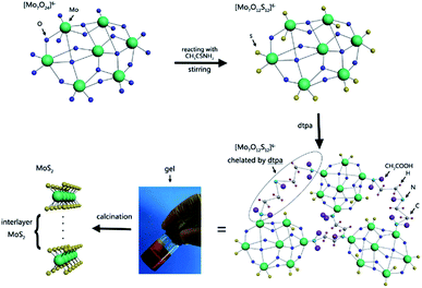
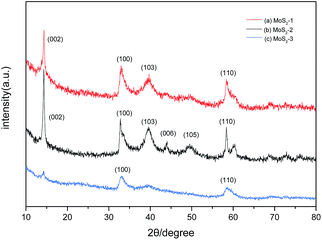
Fig. 1 shows the synthesis mechanism of multilayer MoS2 by chelation-assisted sol–gel method with diethylenetriamine pentaacetic acid (Dtpa) as chelating agent. Firstly, amounts of [Mo7O24]6− ionic groups existed in the neutral solution. [Mo7O24]6− is composed of seven octahedral [MoO6] ionic groups where three different bond lengths exist between Mo and O atoms.39,40 Then the S2− ions provided by CH3CSNH2 substituted for the terminal O atoms combined by Mo–O ionic bond because the bond energy of Mo–S is higher than that of terminal Mo–O. After adding Dtpa into the solution, the chelating agent attacked some new S atoms, broke the Mo–S bonds, and chelated with Mo atoms which lacked electrons to form stable electron structure. In the process, some of the S source were lost in the form of H2S. Every Dtpa molecule connected three Mo atoms of different Mo7O246− ionic groups to form a complicated network structure, which promoted the formation of gel. The wet gel gradually formed at 60 °C in 12 h. Then it transformed into xerogel in two days when the water was totally evaporated and the shrinkage happened in the range between 40% and 60% of the original size. The crystallization of the complex gel was conducted by calcinations at 1000 °C, and the multilayer MoS2 can be facilely obtained.The XRD patterns of as-prepared samples show the precipitates are hexagonal 2H-MoS2 (JCPDS 37-1492) with different crystallinity (Fig. 2). It is obvious that the MoS2-2 sample displays the sharpest diffraction peaks, indicating the highest crystallinity. It reveals that complete MoS2 crystal tends to be formed when the mass ratio of Mo source and S source is 1![[thin space (1/6-em)]](https://www.rsc.org/images/entities/char_2009.gif) :
:![[thin space (1/6-em)]](https://www.rsc.org/images/entities/char_2009.gif) 3. The diffraction peak of MoS2-2 sample at 2θ = 14.2° indicates the MoS2 layers stack orderly along (002) direction with a d-spacing of 0.62 nm. The (100) reflection at 2θ = 33.5° and (110) reflection at 2θ = 59.1° can be found in MoS2-3 sample but no clear (002) reflection. It is supposed that some complicated polysulfide molybdenum were synthesized owing to redundant S source in MoS2-3 sample and few MoS2 layers are stacked in the c direction.16 According to the Scherrer formula, D = Kλ/B
3. The diffraction peak of MoS2-2 sample at 2θ = 14.2° indicates the MoS2 layers stack orderly along (002) direction with a d-spacing of 0.62 nm. The (100) reflection at 2θ = 33.5° and (110) reflection at 2θ = 59.1° can be found in MoS2-3 sample but no clear (002) reflection. It is supposed that some complicated polysulfide molybdenum were synthesized owing to redundant S source in MoS2-3 sample and few MoS2 layers are stacked in the c direction.16 According to the Scherrer formula, D = Kλ/B![[thin space (1/6-em)]](https://www.rsc.org/images/entities/char_2009.gif) cos
cos![[thin space (1/6-em)]](https://www.rsc.org/images/entities/char_2009.gif) θ, K = 0.89, λ = 0.154056 nm, θ = 14.2°, B = 0.507 for MoS2-2 and B = 0.591 for MoS2-1. The average dimension of MoS2 in z-axis is roughly estimated at about 15 nm in MoS2-2 sample corresponding to 25 MoS2 layers, which was facilitated by high-temperature calcination. For MoS2-1 sample, the MoS2 grain dimension in z-axis is about 13 nm, corresponding to 21 MoS2 layers approximately. It shows that the mass ratio of Mo and S plays a role on the formation of multilayer MoS2 to some extent.
θ, K = 0.89, λ = 0.154056 nm, θ = 14.2°, B = 0.507 for MoS2-2 and B = 0.591 for MoS2-1. The average dimension of MoS2 in z-axis is roughly estimated at about 15 nm in MoS2-2 sample corresponding to 25 MoS2 layers, which was facilitated by high-temperature calcination. For MoS2-1 sample, the MoS2 grain dimension in z-axis is about 13 nm, corresponding to 21 MoS2 layers approximately. It shows that the mass ratio of Mo and S plays a role on the formation of multilayer MoS2 to some extent.
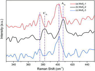
The three samples were further investigated to analyze the inner structure by Raman spectroscopy (Fig. 3). It has been proved that E12g and A1g peaks of monolayer MoS2 appear at 384.3 and 403 cm−1, respectively.17 With the increase of layer numbers, the in-plane E12g vibration weakens and the out-of-plane A1g vibration strengthens. When the layer number is over 6, the E12g and A1g peaks are observed at 382 and 408 cm−1 stably.18,19 It is seen that the MoS2-2 sample exhibits a strong out-of-plane vibration at 408 cm−1 and a relatively weaker in-plane vibration at 382 cm−1. However, the signal of this Raman spectroscopy is a little weak and red shifts are found in MoS2-1 and MoS2-3 samples. It is supposed that amorphous substances and defects in the resultant sample disorder the uniform MoS2 molecule vibrations, thus causing these phenomena. Due to the selection rules for scattering geometry and limited rejection of the Raleigh scattered radiation, the other two vibration modes E1g and E22g could not be detected.20 It proves that the mass ratio of Mo and S also impacts the inner structure of as-prepared MoS2.
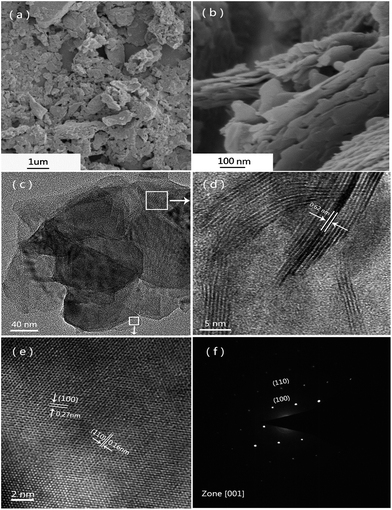
The microstructures and morphologies of as-prepared MoS2-2 sample were observed by SEM and TEM (Fig. 4). It is seen that the MoS2 precipitates exist in the form of particles with the size of <2 μm and some agglomeration (Fig. 4a). Fig. 4b depicts irregular MoS2 flakes aggregate together to form larger particles. As shown in Fig. 4c, the MoS2 nanosheets stack together to form a large flake with different inside thickness. It is clearly observed from Fig. 4d that a nanosheet has some parallel MoS2 crystal fringes with an interlayer distance of 0.62 nm, corresponding to interplanar spacing of 2H-MoS2 (002) plane based on XRD results. The high magnification HR-TEM image of the thin MoS2 layers (Fig. 4e) confirms that the as-prepared MoS2 is typically hexagonal MoS2. The interlayer distance of (100) plane and (110) plane are 0.27 and 0.16 nm, respectively. The selected area electron diffraction (SAED) (Fig. 4f) shows a clear monocrystalline MoS2 diffraction pattern with six inner diffraction spots indicating (100) plane and the outer diffraction spots indicating (110) plane. There is no (002) plane diffraction spots because the electrons incident direction is [001]. Based on above analysis, during the formation of MoS2 particles, large amounts of monocrystalline MoS2 layers in different orientations stacked to form nanosheets, the multilayer nanosheets arranged to form MoS2 flakes, and then the flakes aggregated to construct crystalline MoS2 particles.
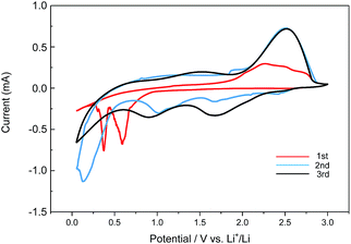
We used the sample MoS2-2 as the negative electrode of lithium ion battery because of its superior structure and composition. Fig. 5 depicts the cyclic voltammetry (CV) profile of as-prepared sample MoS2-2. Cyclic voltammetry is a normal method to research the redox reactions of the electrodes. From Fig. 5, two obvious reduction peaks at 0.6 V and 0.4 V are shown in the first cycle. The peak at 0.6 V implies intercalation of lithium ions into MoS2 layers with MoS2 structure transformation from 2H (trigonal prismatic coordination) to the 1T (octahedral coordination).21–23 The other peak at 0.4 V can be attributed to the conversion reaction process of LixMoS2 into Mo and Li2S. In the anodic sweep, the peak in 2.25 V is attributed to the delithiation of Li2S with the reaction process of Li2S − 2e → 2Li+ + S.7,24,25 In the second and third cathodic sweep, three reduction peaks are found at 1.7 V, 1.0 V, and 0.2 V, respectively, which could be due to the following reactions: 2Li+ + S + 2e → Li2S, MoS2 + xLi+ + xe → LixMoS2, and LixMoS2 + (4 − x)Li+ + (4 − x)e → Mo + 2Li2S.26,27
Fig. 6 shows the first three charge–discharge profiles of the sample MoS2-2 electrodes with a cutoff voltage of 0.005–3 V at a current density of 100 mA g−1, which are nearly accord with the CV measurements described above. In the first discharge process, there are two obvious voltage plateaus at 0.5 V and 1.0 V, which indicates the formation of LixMoS2 and the following conversion reaction of LixMoS2 into Mo and Li2S.1,17,28 The slope region below 0.5 V could be attributed to the formation of a solid-electrolyte interphase (SEI) layer.29,30 In the second and third discharge process, three vague potential plateaus could be found at 1.7 V, 1.0 V and 0.25 V, which are in qualitative agreement with the CV results. In the charge process, the MoS2-2 electrode shows a distinct potential plateaus at 2.25 V, which could be due to the reduction of sulfur to polysulfide.24,31,32 Fig. 6 also shows that the MoS2-2 electrode delivers an initial discharge capacity of 1149 mA h g−1 and a reversible charge capacity of 1038 mA h g−1, with a high coulombic efficiency of 90.3%.
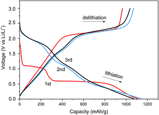 | ||
| Fig. 6 Galvanostatic charge and discharge curves of as-prepared sample MoS2-2 at a current density of 100 mA g−1. | ||
Fig. 7a depicts the cycling behavior and rate capability of the sample MoS2-2 at a constant current density of 100 mA g−1. Although the first charge and discharge capacities are higher than 900 mA h g−1, the cycling stability of the MoS2-2 electrode is poor with a discharge capacity decrease from 947 to 353 mA h g−1 after 40 cycles. Fig. 7b shows the rate cycling behavior of the sample MoS2-2 electrode. At the current densities of 1.0 A g−1, the capacity rapidly declines below 300 mA h g−1, which cannot compete with the MoS2/graphene composite electrode with good rate performance. Surprisingly, the sample MoS2-2 electrode has a high coulombic efficiency of nearly 100%.
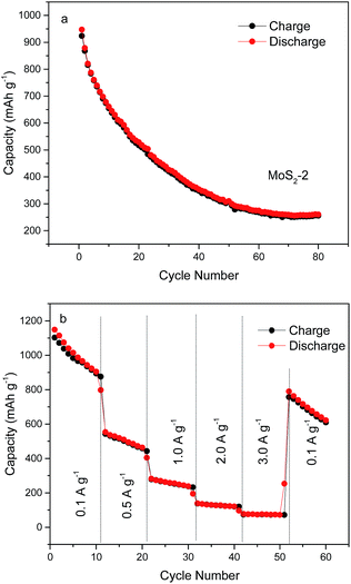 | ||
| Fig. 7 (a) Cycle performance of as-prepared sample MoS2-2 electrode at a current density of 0.1 A g−1, and (b) their rate capabilities at different current densities. | ||
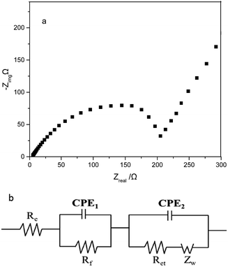
Electrochemical impedance spectra (EIS) can be applied to better understand the electrochemical performance of MoS2 electrode. Fig. 8a depicts the Nyquist plots of MoS2-2 electrode after 40th cycle, and Fig. 8b is the equivalent circuit model for the impedance response. The semicircle in high-frequency region is due to the resistance Rf and CPE1 of the solid electrolyte interphase (SEI) film.33,34 The medium-frequency semicircle corresponds to the charge-transfer resistance Rct and CPE2 of the electrode/electrolyte interface.35,36 The inclined line is assigned to the lithium-diffusion within the electrode material.37 According to EIS equivalent circuit in Fig. 8b, Rf and Rct of MoS2-2 electrode are 14.84 and 121.9 Ω, respectively.
4. Conclusions
In summary, the multilayer MoS2 crystal was synthesized by a chelation-assisted sol–gel method followed by calcination. Diethylenetriamine pentaacetic acid (Dtpa) as chelation agent was introduced to react with Mo and S sources to form Mo–S chelated gel. The mass ratio of Mo and S affected the formation of multilayer MoS2 as well as the inner structure of MoS2, and the best crystalline MoS2 particles are obtained with the Mo and S mass ratio of 1![[thin space (1/6-em)]](https://www.rsc.org/images/entities/char_2009.gif) :
:![[thin space (1/6-em)]](https://www.rsc.org/images/entities/char_2009.gif) 3. The resultant crystalline MoS2 particles were constructed by irregular MoS2 flakes arranged together, while these flakes were formed by adjustable MoS2 layers stacked together. The electrochemical tests showed the possibility of as-prepared MoS2 applied as negative electrode for lithium ion batteries. In order to improve the electrochemical performance, we need to continually explore a sol–gel process to prepare MoS2/graphene composite with the aid of synergy effect between MoS2 and graphene and the superior electron conductivity of graphene.
3. The resultant crystalline MoS2 particles were constructed by irregular MoS2 flakes arranged together, while these flakes were formed by adjustable MoS2 layers stacked together. The electrochemical tests showed the possibility of as-prepared MoS2 applied as negative electrode for lithium ion batteries. In order to improve the electrochemical performance, we need to continually explore a sol–gel process to prepare MoS2/graphene composite with the aid of synergy effect between MoS2 and graphene and the superior electron conductivity of graphene.
Acknowledgements
This work is supported by the National Natural Science Foundation of China (51372225) and High Science & Technique Brainstorm Project of Zhejiang Province of China (No. 2017C01002).References
- Z. Wang, T. Chen, W. Chen, K. Chang, L. Ma, G. Huang, D. Chen and J. Y. Lee, J. Mater. Chem. A, 2013, 1, 2202 CAS.
- M. A. Worsley, S. J. Shin, M. D. Merrill, J. Lenhardt, A. J. Nelson, L. Y. Woo, A. E. Gash, T. F. Baumann and C. A. Orme, ACS Nano, 2015, 9, 4698 CrossRef CAS PubMed.
- A. K. Geim and I. V. Grigorieva, Nature, 2013, 499, 419 CrossRef CAS PubMed.
- Q. H. Wang, K. Kalantar-Zadeh, A. Kis, J. N. Coleman and M. S. Strano, Nat. Nanotechnol., 2012, 7, 699 CrossRef CAS PubMed.
- S. J. Ding, D. Y. Zhang, J. S. Chen and X. W. Lou, Nanoscale, 2012, 4, 95 RSC.
- L. Lin, N. Miao, Y. Wen, S. Zhang, P. Ghosez, Z. Sun and D. A. Allwood, ACS Nano, 2016, 10, 8929 CrossRef CAS PubMed.
- M. Acerce, D. Voiry and M. Chhowalla, Nat. Nanotechnol., 2015, 10, 313 CrossRef CAS PubMed.
- Z. Hu, L. Wang, K. Zhang, J. Wang, F. Cheng, Z. Tao and J. Chen, Angew. Chem., 2014, 53, 12794 CrossRef CAS PubMed.
- J. Brivio, D. T. Alexander and A. Kis, Nano Lett., 2011, 11, 5148 CrossRef CAS PubMed.
- X. L. Li and Y. D. Li, Chemistry, 2003, 9, 2726 CrossRef CAS PubMed.
- L. Ma, W.-X. Chen, Z.-D. Xu, J.-B. Xia and X. Li, Nanotechnology, 2006, 17, 571 CrossRef CAS.
- H. Lin, X. Chen, H. Li, M. Yang and Y. Qi, Mater. Lett., 2010, 64, 1748 CrossRef CAS.
- W.-J. Li, E.-W. Shi, J.-M. Ko, Z.-z. Chen, H. Ogino and T. Fukuda, J. Cryst. Growth, 2003, 250, 418 CrossRef CAS.
- X. Guo, Q. Zhang, X. Ding, Q. Shen, C. Wu, L. Zhang and H. Yang, J. Sol-Gel Sci. Technol., 2016, 79, 328 CrossRef CAS.
- N. Li, Y. Chai, B. Dong, B. Liu, H. Guo and C. Liu, Mater. Lett., 2012, 88, 112 CrossRef CAS.
- X. Y. Zhao, C. W. Hu and M. H. Cao, Chem.–Asian J., 2013, 8, 2701 CrossRef CAS PubMed.
- L. Ma, X. Zhou, L. Xu, X. Xu, L. Zhang and W. Chen, Electrochim. Acta, 2015, 167, 39 CrossRef CAS.
- C. Lee, H. Yan, L. E. Brus, T. F. Heinz, J. Hone and S. Ryu, ACS Nano, 2010, 4, 2695 CrossRef CAS PubMed.
- G. L. Frey, R. Tenne, M. J. Matthews, M. S. Dresselhaus and G. Dresselhaus, Phys. Rev. B: Condens. Matter Mater. Phys., 1999, 60, 2883 CrossRef CAS.
- J. L. Verble, T. J. Wietling and P. R. Reed, Solid State Commun., 1972, 11, 941 CrossRef CAS.
- L. Ma, J. Ye, W. Chen, J. Wang, R. Liu and J. Y. Lee, ChemElectroChem, 2015, 2, 538 CrossRef CAS.
- T. Stephenson, Z. Li, B. Olsen and D. Mitlin, Energy Environ. Sci., 2014, 7, 209 CAS.
- C. Zhu, X. Mu, P. A. van Aken, Y. Yu and J. Maier, Angew. Chem., 2014, 53, 2152 CrossRef CAS PubMed.
- W. F. Li, Y. M. Yang, G. Zhang and Y. W. Zhang, Nano Lett., 2015, 15, 1691 CrossRef CAS PubMed.
- K. Chang and W. Chen, Chem. Commun., 2011, 47, 4252 RSC.
- K. Chang, W. Chen, L. Ma, H. Li, H. Li, F. Huang, Z. Xu, Q. Zhang and J.-Y. Lee, J. Mater. Chem., 2011, 21, 6251 RSC.
- K. Chang and W. X. Chen, ACS Nano, 2011, 5, 4720 CrossRef CAS PubMed.
- L. Fei, Y. Xu, X. Wu, G. Chen, Y. Li, B. Li, S. Deng, S. Smirnov, H. Fan and H. Luo, Nanoscale, 2014, 6, 3664 RSC.
- D. Xie, W. J. Tang, X. H. Xia, D. H. Wang, D. Zhou, F. Shi, X. L. Wang, C. D. Gu and J. P. Tu, J. Power Sources, 2015, 296, 392 CrossRef CAS.
- K. S. Kumar, W. Li, M. Choi, S. M. Kim and J. Kim, Chem. Eng. J., 2016, 285, 517 CrossRef CAS.
- S. Hu, W. Chen, J. Zhou, F. Yin, E. Uchaker, Q. Zhang and G. Cao, J. Mater. Chem. A, 2014, 2, 7862 CAS.
- P. Sun, W. Zhang, X. Hu, L. Yuan and Y. Huang, J. Mater. Chem. A, 2014, 2, 3498 CAS.
- Z. Deng, Y. Hu, D. Ren, S. Lin, H. Jiang and C. Li, Chem. Commun., 2015, 51, 13838 RSC.
- W. J. Zhu, H. Yang, W. K. Zhang, H. Huang, X. Y. Tao, Y. Xia, Y. P. Gan and X. Z. Guo, RSC Adv., 2015, 5, 74774 RSC.
- H. Li, K. Yu, H. Fu, B. Guo, X. Lei and Z. Zhu, J. Phys. Chem. C, 2015, 119, 7959 CAS.
- W. J. Zhu, H. Yang and X. Z. Guo, RSC Adv., 2016, 6, 13505 RSC.
- T. S. Sahu and S. Mitra, Sci. Rep., 2015, 5, 12571 CrossRef CAS PubMed.
- Z. Wang, T. Chen, W. X. Chen and J. Y. Lee, J. Mater. Chem. A, 2013, 1, 2202 CAS.
- A. Muller, S. Sarkar and M. Dartmann, Angew. Chem., 1978, 90, 535 Search PubMed.
- W. L. Lindsay and W. A. Norvell, Soil Sci. Soc. Am. J., 1978, 42, 421 CrossRef CAS.
| This journal is © The Royal Society of Chemistry 2017 |

