 Open Access Article
Creative Commons Attribution 3.0 Unported Licence
A simple process step for tuning the optical emission and ultraviolet photosensing properties of sol–gel ZnO film
Shuvaraj Ghosh and
Durga Basak*
Department of Solid State Physics, Indian Association for the Cultivation of Science, Jadavpur, Kolkata 700032, India. E-mail: sspdb@iacs.res.in
First published on 3rd January 2017
Abstract
A simple process step involving controlled cooling action was successfully established for defect control in a sol–gel ZnO film. In this study, a sol–gel process was adapted to form two sets of ZnO films with two different pre-heat treatment temperatures (set A and set B), but with the same post-heat treatment temperatures subjected to three different cooling rates (0.12, 0.25 and 90 °C s−1) for each set in order to control the defect formation. The structural and surface morphological results showed that ZnO films, for both the sets, exhibited a wurtzite structure, whereas the crystallite orientations, FWHM of the (002) peak and the surface roughness, were found to vary with the cooling rate irrespective of the pre-heat treatment temperature. The films showed phenomenal changes in the photoluminescence (PL) and ultraviolet photoconductivity (PC) results. Irrespective of the set type, the rapidly cooled (90 °C s−1) films showed an improved ultraviolet-to-visible PL intensity ratio as compared to others as a result of reduced defect emission in the visible region. The dark and photo current measurement results indicated the existence of higher adsorbed O2 molecules-related trap states and an enhanced UV photoresponse in rapidly cooled films for both the sets, providing strong evidence in support of defect control. X-ray photoelectron spectroscopy results confirmed the presence of larger adsorbed O2 molecules at the strained oxygen vacancy sites in the rapidly cooled films. These results demonstrated that the post-heat treatment cooling rate could be a brilliant and easy pathway to control the defects for tuning the optical emission and ultraviolet photosensing properties of sol–gel ZnO films.
Introduction
ZnO, II–VI semiconductor material belonging to the wurtzite family, has a wide range of applications, from skin care, phosphors, and varistors to transparent electrodes in displays, piezoelectric devices and the biomedical field.1–5 This oxide material has received significant attention due to its application in optoelectronic devices, such as UV detectors, LEDs and LDs, for its direct and wide band gap of 3.37 eV at room temperature.6–10 Under above band gap photoexcitation, ZnO radiates light in the UV region at around 380 nm. This photoluminescence in the UV region is due to recombination of excitons as ZnO has a very large exciton binding energy of about 60 meV, making the excitons stable at room temperature.11–13 Therefore, ZnO is a very important material for UV light emission and laser diodes. In addition to the sharp and strong UV emission, a broad peak in the visible region is found in almost all ZnO grown irrespective of the growth technique. The nature and intensity of the visible emission has been the subject of immense research for decades since the origin of the visible emission is not conclusively clear yet. Oxygen vacancies (VO) and other intrinsic defects have been thought to be responsible for these visible bands in addition to some impurities such as Cu2+.14–17 However, these assignments have always become difficult due to complex origin of the defects as well as more than one of the defects being responsible for an emission. For example, it has been proposed that holes can be trapped at the surface and that the green emission is due to the recombination of excited electrons with these deeply trapped holes.18 However, it is well understood that both UV and visible emissions strongly depend on the surface states as the surface depletion width, controlled by the defect concentration, influences both emission intensities. Therefore, a controlled processing is necessary to adjust the surface states in order to maximise the UV and minimise the visible emission. Towards this effort, there have been numerous reports on enhanced UV emission and/or UV/VIS emission ratio using doping,19,20 surface modification,21 changing the surface/volume ratio, etc. However, doping and surface modification involve either an extra dopant source or a further coating step. A growth method itself that is capable of controlling the emission property of ZnO films is highly desirable.ZnO thin films were prepared using various growth techniques, such as RF magnetron sputtering,22–24 chemical vapor deposition,25 pulsed laser deposition (PLD),26 spray pyrolysis,27 photo-atomic layer deposition,28 metal organic chemical vapor deposition (MOCVD),29 molecular beam epitaxy (MBE)30 and sol–gel technique.31 The sol–gel process has several advantages over others due to its simplicity, excellent compositional control, safety, low cost of the apparatus and raw materials, homogeneity on the molecular level due to the mixing of liquid precursors and relatively lower crystallization temperature. ZnO thin film deposition by the sol–gel method requires a heat treatment in air at higher temperatures in order to oxidise the precursors of the zinc compound solution. In general, the heat treatment involves two steps: drying at lower temperatures to evaporate the organic solvents (known as pre-heat treatment), and at higher temperatures for the formation of ZnO (known as post-heat treatment). The drying temperature is often chosen such that it is good for solvent evaporation, organic compounds removal as well as close to the ZnO crystallization temperature. Therefore, a temperature range from 120 °C to 350 °C was chosen for the pre-heat treatment process.32 The temperature for post-heat treatment was chosen in the range of 500–600 °C. It is also well known that the properties of ZnO films, deposited by the sol–gel technique, are determined by various parameters, such as precursor type and concentration, aging time, substrate, annealing temperature, and thickness.33 Kim et al. have applied two different cooling rates for preparing ZnO films, one slow and one fast after the pre-heat treatment at 300 °C, followed by a post-heat treatment at 550 °C. Along with a detailed morphological change, they have reported a blue shift and higher intense UV near band edge (NBE) peak for the film that was cooled rapidly. However, the post-heat treatment is very important as it is the step when the ZnO crystallites are formed. The cooling step after the post-heat treatment is thus very crucial and appears to be an important factor that largely controls the surface properties, which has been rarely reported. Therefore, in the present study, we demonstrate a simple, low temperature, and low-cost technique for controlling the photoluminescence (PL) and UV photoconductivity (PC) properties of ZnO thin films. It was shown that irrespective of the pre-heat treatment temperature, a rapidly cooled film always showed a higher UV/VIS emission ratio compared to slowly cooled or normally cooled films due to defect control; this has been supported by the results of (PC) studies. This study paves a way through comprehensive and comparative PL and PC studies of process controlled sol–gel ZnO films that can be exploited to tune the optical emission properties and photo-assisted conductivity of other oxides too.
Experimental
ZnO thin films were deposited on glass substrates using a sol–gel spin coating method. The glass substrates were cleaned and degreased ultrasonically using chromic solution, de-ionized water, HCl and KOH, followed by acetone and methanol for 10 min each. The sol concentration was 0.1 M, which was prepared by adding the required amount of zinc acetate-dihydrate [Zn(CH3COO)2·2H2O] with dehydrated isopropyl alcohol. Diethanolamine (DEA) was added to the solution as a sol stabilizer, followed by a thorough mixing with a magnetic stirrer at a speed of 400 rmp at room temperature (RT) for two hours and was kept for 48 hours for aging. Two sets of films were prepared wherein the pre-heat treatment after coating was varied while keeping the post-heat treatment and thereafter the cooling steps exactly similar.For set A films
The substrates were spin coated with the sol at 2500 rpm and after each coating process, the substrates were dried at 120 °C for 10 minutes and then crystallized at 500 °C for 30 min in air. The coating process was repeated 20 times. The final post-heat treatment was carried out at 500 °C for 1 h in air.For set B films
The substrates were spin coated with the sol at 2500 rpm and after each coating process, the substrates were dried at 120 °C for 10 minutes and then crystallized at 350 °C for 20 min in air. The coating process was repeated 20 times. Similar to set A, the final post-heat treatment was carried out at 500 °C for 1 h in air.Cooling processes after the final post-heat treatment for both set A and set B films were varied as described below:
(1) Slow cooling (sample A1 and B1): the ZnO films were taken out from the furnace very slowly and cooled to RT. The average cooling rate was 0.12 °C s−1.
(2) Normal cooling (sample A2 and B2): the ZnO films were taken out from furnace after annealing and kept at RT for cooling. The average cooling rate was 0.25 °C s−1.
(3) Fast cooling (sample A3 and B3): the ZnO films were taken out from furnace and dropped very quickly into a container filled with liquid N2. The average cooling rate was 90 °C s−1.
The purpose of varying the pre-heat treatment temperature while keeping the post-heat treatment temperature and thereafter the cooling steps exactly similar was to verify if the cooling rate affects the properties of ZnO films even when a different procedure is adopted for the film preparation. The summary of the entire growth technique for both the sets is shown in the following flow chart (Scheme 1).
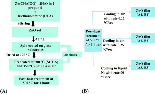 | ||
| Scheme 1 Flow chart for preparation of ZnO films up to post-heat treatment (A) and different cooling steps after post-heat treatment (B). | ||
The crystalline phase of the ZnO film was determined by an X-ray diffractometer (XRD) (model: X'pert pro, PANalytical) with CuKα radiation (1.5418 Å). The surface texture and roughness were measured via field emission scanning electron microscopy (FESEM; model no. JEOL JSM-6700) and atomic force microscopy (AFM; VEECO model: diCP-II). For the measurement of PL property of the films at RT, an He–Cd laser (Kimmon Koha Co. Ltd.; model: KR1801C) with optical excitation line at 325 nm and a high-resolution spectrometer (Horiba Jobin Yvon, model: iHR 320) together with a photomultiplier tube were used. X-ray photoelectron spectroscopy (XPS, Omicron, serial no: 0571) results were studied to know the chemical states of the elements and contribution of surface adsorbed –OH group and O2 in the films. For dark and photocurrent measurements, two Al electrodes (1 mm diameter) of thickness about 40–60 nm separated by a 3 mm distance were evaporated onto ZnO films by a thermal evaporator (model: 12A4D, HHV). The direct currents between the two contacts were measured using a Keithley sourcemeter (model: 2400) and GPIB data transfer card. For photoresponse measurements, the photocurrents were measured by illuminating the film with a light wavelength 325 nm from a He–Cd laser source at a 10 V bias voltage. The films were kept in the dark for several hours to achieve the equilibrium before the dark current measurements. The photocurrent transients were measured under chopped illumination (420 s on and 600 s off) of UV light (325 nm, 35–40 mW), and the current value at 10 V applied bias at RT was measured simultaneously.
Results and discussion
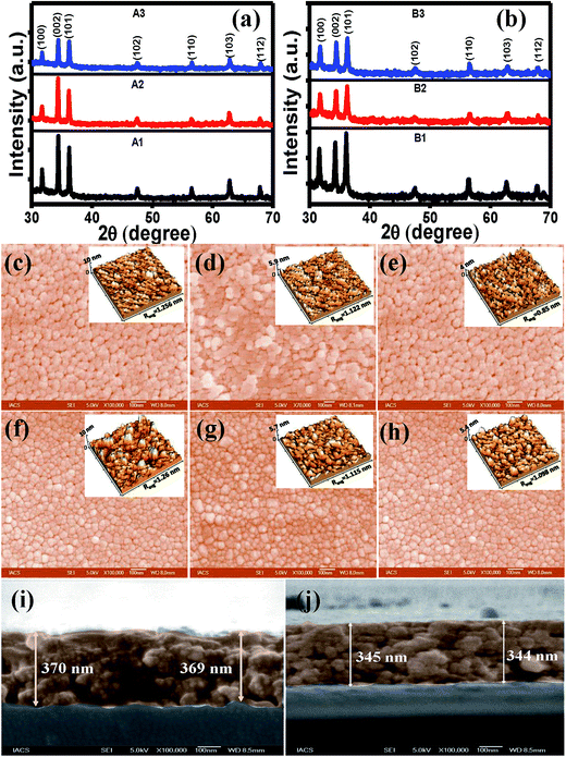
The XRD patterns for all the films as presented in Fig. 1(a) and (b) showed multiple peaks due to (100), (002), (101), (102), (110), (103) and (112) planes of reflections for a single phase wurtzite structure of ZnO indicating random orientations of the crystallites. Considering the three major peaks, it is seen that orientations of the crystallites along (002) was quite higher than that along (100) and (101) planes for both set A and B films. FWHM value of the (002) peak was maximum for the B3 film, whereas it was minimum for the A3 film. A variety of factors can contribute to the width of an X-ray diffraction peak in addition to instrumental effects and crystallite size; the most important of these are usually inhomogeneous strain, crystal lattice imperfections such as dislocations, stacking faults, twinning, grain boundaries, sub-boundaries, chemical heterogeneities, and crystallite smallness.34 Therefore, a higher FWHM value of the B3 sample indicated poorer crystallinity as a result of rapid cooling. The ZnO formation procedures for set A and set B were different since the sols were subjected to different heat treatment. The XRD results of set B films indicated that heat treatment was the determining factor for the structural qualities. As the film cools, the film and the substrate contract in different amounts, displaying different thermal expansion coefficients, and thus a thermal strain is created in the film.35 The strain along the c axis, ε is given by the following equation:36| ε = (C − C0)/C0 × 100% | (1) |
| Sample type | FWHM (002) | Strain ε (%) | Average roughness (nm) |
|---|---|---|---|
| A1 | 0.250 | −0.225 | 1.256 |
| A2 | 0.242 | −0.184 | 1.122 |
| A3 | 0.241 | −0.163 | 0.85 |
| B1 | 0.226 | −0.242 | 1.26 |
| B2 | 0.249 | −0.158 | 1.115 |
| B3 | 0.262 | −0.134 | 1.098 |
The optical band gaps of the films are calculated from the transmission graph of the films using the fundamental absorption equation:40
| (αhν)1/n = A(hν − Eg) | (2) |
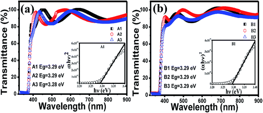 | ||
| Fig. 2 Transmittance spectra of (a) set A and (b) set B films. The corresponding insets show the Tauc plots of a representative film and the values of band gaps estimated from the Tauc plots. | ||
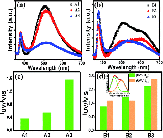
The PL spectra of all the films in Fig. 3(a) and (b) show that there is a sharp and intense UV peak at around 379 nm, which is attributed to the band-edge excitonic emission and a broad peak at around 500 nm attributed to sub-band gap defects. Regardless of the exact origin of the visible emissions, the large visible PL intensity for the films A1 and A2 indicates that the films are rich in defects. In contrast to set A, the set B films also showed a more intense UV peak than the visible broad peak. The change in the PL properties was probably due to the difference in the heat treatment, as previously mentioned. However, it was noticed that for both the sets, as the cooling rate was controlled, the magnitude of the UV peak of the films remained almost unchanged, whereas the relative magnitude of the visible peak changed widely under the same experimental set-up and condition for the PL measurements. Similar change in the PL properties was observed for TiO2 films.42 The line shape of the visible peak for set B films is evidenced as the superposition of two peaks at around 500 nm (green luminescence, GL) and one at around 600 nm (orange-red luminescence, ORL). Therefore, we have fitted the broad peak into two peaks (GL and ORL), and in order to compare their intensities with the UV peak intensity, both IUV/IVIS(GL) and IUV/IVIS(ORL) values for set B films were evaluated. The values of IUV/IVIS (Fig. 3(c) and (d)) were varied widely for the films processed under different cooling conditions. For N2 cooled films for both sets, the value of IUV/IVIS is the maximum as compared to the other two films in the respective series (Fig. 3(c) and (d)). However, a 4-fold increase in the IUV/IVIS value in A3 as compared to A1 could not be accounted for by the small change in the thickness of the film alone (Fig. 1(i) and (j)). The weaker defect emission intensity implies that the concentration of defects contributing to the radiative recombination for the green emission was very low. Due to rapid cooling, probability of adsorbed OH on the surface of the film was much less (since –OH is generally absorbed at ∼150 °C) than the two other films.43 Therefore, from the experimental evidence, it may be mentioned that this surface adsorbed species indirectly control the green emission. To know the exact mechanism, the possible origins of the GL need to be analyzed further.
Several studies have been published regarding the origin of this band, using different experimental setups and different samples grown using various techniques. There may be multiple origins of this luminescence because different transitions can lead to quite similar luminescence emission wavelengths, thereby generating a great controversy about the GL in ZnO. There are several hypotheses citing widely varied origins of GL, such as, zinc vacancies (VZn), oxygen vacancies (VO), interstitial zinc ions (Zni), oxygen antisites ZnO, transitions from Zni to VZn, and impurity of Cu2+ ions.14–17,23,44–48 Recently, it was recognized that VZn is a widely accepted defect to contribute to this green wavelength.43 VZn are situated 0.9 eV above the valence band minima, and hence a transition from the conduction band (or from a shallow donor) would yield a luminescence around 2.4 eV, which corresponds to the GL observed in ZnO samples grown using several techniques. It is likely that the surface adsorbed species generally heal the defects like VO or VZn.49 Since surface adsorbed –OH species in rapidly cooled films is expected to be quite low, healing of the VZn defects is also less probable, which means that these defects would satisfy their paring with other native defects forming complex defects such as VZn–Zni Frenkel pair.50 VZn is likely to form stable complexes with shallow donors in ZnO.51 However, the defect complex of VZn together with the shallow donor Zni (VZn + Zni) is a possible candidate for the orange luminescence (OL).52 GL was reduced in our study implying the probability of the defect complex to act as a radiative recombination centre for YL, and GL is supposedly less probable due to lesser compressive strain developed in the films. This has further implications that either of the individual defects plays a key role in GL. Previously it has been reported that heat treatment temperature and ambient temperature both control the ZnO film properties.53 In addition, irrespective of the heat treatments to form ZnO, a simple process, such as a cooling step applied after the post-heat treatment, is very much steering to tune its luminescence properties. A similar type of treatment was used by M. S. Kim et al. and they got a higher UV/VIS emission ratio for fast cooling. Compared with our results, their fast cooled sample showed much less visible emission, which indicates that their sample was completely healed by this treatment.
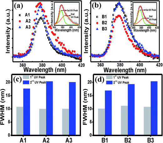
Further analyses of the UV peak in Fig. 4(a) and (b) showed that the UV peak for the both sets A and B were asymmetric on the higher wavelength side which was perfectly fitted with two Gaussian peaks, as shown in the respective insets in the figures. The higher energy peak corresponds to the exciton recombination (1st UV), whereas the lower energy peak at around 388 nm is known to arise due to the recombination from the Zni donor to the valence band.54 While the FWHM of the first UV peak remains almost unchanged irrespective of the cooling rate, the values for the second UV peak show a general increasing trend as the cooling rate is increased (Fig. 4(c) and 4(d)), indicating more spread of the energy level of the Zni defects below the conduction band. This experimental result indicates that Zni might have an attractive interaction with VZn in the complex defects, as mentioned earlier.
The linear increase in the current with the bias voltage in the I–V curves of the films for both sets (Fig. 5(a) and (b)) indicate an ohmic nature of the contacts with ZnO film. It was found that the dark currents for A3 and B3 were lower by two orders of magnitude than the other two in the series, whereas the value of the photocurrent did not differ much. It is known that VZn does not contribute to p-type conductivity in ZnO, but rather acts as a deep compensating center.55,56 If it had been the compensating centres, the magnitude of the photocurrent should not have been similar. Therefore, the presence of only VZn is ruled out. The dark current largely depends on the surface adsorbed O2 molecules.57 Therefore, from the results it can be inferred that A3 and B3, i.e. rapidly cooled films, might have a higher number of adsorbed O2 molecules, which may be attributed to the change in the strain values. The effect of strain on the adsorption of chemisorbed particles on surfaces offers a means of manipulating adsorption properties quite significantly. In an experimental study by Gsell et al.,58 the preferential occupation of local areas with expanded lattices, as well as the depletion of compressed lattice areas, was demonstrated for O2 molecules adsorbed on Ru (0001). The photocurrent transient curves in Fig. 5(c) and (d) show that as soon as UV light (325 nm and power 35–40 mW) was shined, the current increased very fast and when the light was turned ‘Off’, the current dropped. The recovery process in thin films is always slower than the response, as shown in earlier reports.59,60 This is due to the carrier trapping at the defects sites. The photo-to-dark current value i.e. the UV photoresponsivity value was much higher in both the A3 and B3 films, making them good UV photosensors. Such a high photo-to-dark current ratio has not been reported earlier for sol–gel ZnO films.61 For both sets of films, the current did not attain the dark value; this is consistent with the persistent photoconductivity (PP) phenomenon that is similar to previous reports.32
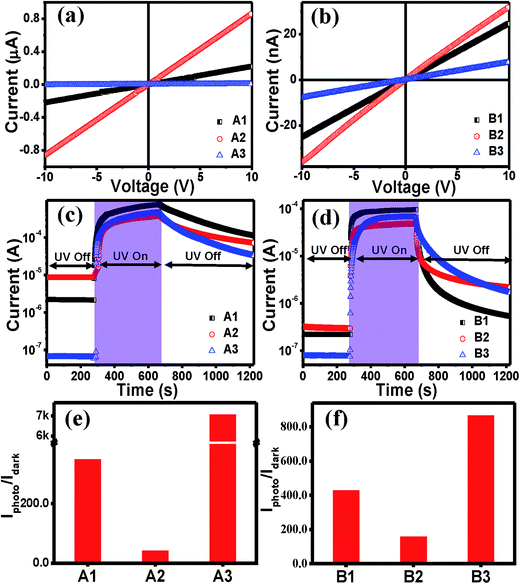 | ||
| Fig. 5 Dark I–V curves of (a) set A and (b) set B films. Photocurrent transients for (c) set A and (d) set B films. The photo-to-dark current ratios of (e) set A and (f) set B films. | ||
Having known that –OH could not get absorbed and the presence of more adsorbed O2 on the surface of the ZnO films of rapidly cooled films, the XPS tool was used to investigate the O content of the films. The XPS full scan for the films of set A and B show signals for only Zn, O and C elements (Fig. 6), indicating no other impurities in the samples. The O 1s core level peak was deconvoluted well into three peaks for A2 and into two peaks for A3. The peak centered at 530.4 ± 0.3 eV is associated with the O2− ions in the wurtzite structure surrounded by the Zn atoms with the full supplement of nearest-neighbour O2− ions.62 The peak at 531.5 ± 0.3 eV is associated with O2− ions that are in the oxygen-deficient regions within the ZnO matrix.62 The peak at 532.3 ± 0.3 eV is attributed to chemisorbed or dissociated O2 or –OH species on the surface of the ZnO thin film, such as –CO3, adsorbed H2O or adsorbed O2.62 It is very interesting to note that in contrast to A2 and B2, for both A3 and B3 films, the O 1s peak could be fitted with two peaks showing more O content (more relative peak area) possibly due to the more adsorbed O2 molecules at the less strained O vacancy sites.63 Therefore the XPS results clearly indicate and support tuning the defects by simply controlling the cooling step.
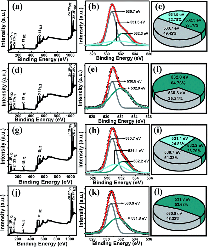 | ||
| Fig. 6 XPS full scan of (a) A2, (d) A3, (g) B2, (j) B3 films. Deconvoluted O 1s1/2 peak of (b) A2 (e) A3 (h) B2 (k) B3. Pie-chart of the relative peak areas (c) A2, (f) A3, (i) B2, (l) B3 films. | ||
Conclusion
In conclusion, we have shown a simple, straight forward and quick way to control the defects to tune the optical emission and ultraviolet photosensing properties of sol–gel ZnO films. Improving the PL properties as an enhanced UV/VIS emission intensity ratio was demonstrated in the rapidly cooled films irrespective of the pre-heat treatment procedure. Not only photoluminescence, but highly enhanced UV photoresponse due to higher O2 molecule adsorption on ZnO surface was observed in the rapidly cooled films. Our results give an insight into the importance of a simple process step for controlling the photoluminescence and photoconductivity properties with an eye on practical applications.Acknowledgements
One of the authors, S. Ghosh would like to thank CSIR, India for providing the fellowship vide Ref no: 22/12/2013(ii)EU-V.References
- S. H. Hsu, Y. Y. Lin, S. Huang, K. W. Lem, D. H. Nguyen and D. S. Lee, Nanotechnology, 2013, 24, 475102 CrossRef PubMed.
- A. A. Mosquera, D. Horwat, A. Rashkovskiy, A. Kovalev, P. Miska, D. Wainstein, J. M. Albella and J. L. Endrino, Sci. Rep., 2013, 3, 1714 Search PubMed.
- S. Dhara and P. K. Giri, Nanoscale Res. Lett., 2011, 6, 504 CrossRef PubMed.
- S. F. Varol, G. Babur, G. Cankaya and U. Kolemen, RSC Adv., 2014, 4, 56645–56653 RSC.
- A. Mallick, A. Kole, T. Ghosh, P. Chaudhuri and D. Basak, Sol. Energy, 2014, 108, 80–87 CrossRef CAS.
- A. I. Inamdar, S. H. Mujawar, S. R. Barman, P. N. Bhosale and P. S. Patil, Semicond. Sci. Technol., 2008, 23, 085013 CrossRef.
- B. Pare, P. Singh and S. B. Jonnalgadda, J. Sci. Ind. Res., 2009, 68, 724–729 CAS.
- C. Soci, A. Zhang, B. Xiang, S. A. Dayeh, D. P. R. Aplin, J. Park, X. Y. Bao, Y. H. Lo and D. Wang, Nano Lett., 2007, 7, 1003–1009 CrossRef CAS PubMed.
- S. Kiruthika, S. Singh and G. U. Kulkarni, RSC Adv., 2016, 6, 44668–44672 RSC.
- R. Paul, R. N. Gayen, S. Biswas, S. V. Bhat and R. Bhunia, RSC Adv., 2016, 6, 61661–61672 RSC.
- J. G. Lu, Z. Z. Ye, Y. Z. Zhang, Q. L. Liang, S. Fujita and Z. L. Wang, Appl. Phys. Lett., 2006, 89, 023122 CrossRef.
- S. A. Ansari, M. M. Khan, S. Kalathil, A. Nisar, J. Lee and M. H. Cho, Nanoscale, 2013, 5, 9238–9246 RSC.
- N. Gogurla, A. K. Sinha, S. Santra, S. Manna and S. K. Ray, Sci. Rep., 2014, 4, 6483 CrossRef CAS PubMed.
- R. Dingle, Phys. Rev. Lett., 1969, 23, 579–581 CrossRef CAS.
- Y. I. Alivov, M. V. Chukichev and V. A. Nikitenko, Semiconductors, 2004, 38, 31–35 CrossRef CAS.
- F. H. Leiter, H. R. Alves, A. Hofstaetter, D. M. Hofmann and B. K. Meyer, Phys. Status Solidi B, 2001, 226, R4–R5 CrossRef CAS.
- F. Leiter, H. Alves, D. Pfisterer, N. G. Romanov, D. M. Hofmann and B. K. Meyer, Phys. B, 2003, 340, 201–204 CrossRef.
- S. Wilken, J. Parisi and H. Borchert, J. Phys. Chem. C, 2014, 118, 19672–19682 CAS.
- Z. C. Pan, X. L. Tian, S. K. Wu, C. M. Xiao, Z. L. Li, J. F. Deng, G. H. Hu and Z. G. Wei, Superlattices Microstruct., 2013, 54, 107–117 CrossRef CAS.
- Z. C. Pan, P. W. Zhang, X. L. Tian, G. Cheng, Y. H. Xie, H. C. Zhang, X. F. Zeng, C. M. Xiao, G. H. Hu and Z. G. Wei, J. Alloys Compd., 2013, 576, 31–37 CrossRef CAS.
- L. Chen, T. T. Tran, C. A. Huang, J. Z. Li, L. J. Yuan and Q. Y. Cai, Appl. Surf. Sci., 2013, 273, 82–88 CrossRef CAS.
- S. Sharma, S. Vyas, C. Periasamy and P. Chakrabarti, Superlattices Microstruct., 2014, 75, 378–389 CrossRef CAS.
- S. Dhara and P. K. Giri, Thin Solid Films, 2012, 520, 5000–5006 CrossRef CAS.
- N. Srinatha, Y. S. No, V. B. Kamble, S. Chakravarty, N. Suriyamurthy, B. Angadi, A. M. Umarji and W. K. Choi, RSC Adv., 2016, 6, 9779–9788 RSC.
- Q. J. Feng, S. Liu, Y. Liu, H. F. Zhao, J. Y. Lu, K. Tang, R. Li, K. Xu and H. Y. Guo, Mater. Sci. Semicond. Process., 2015, 29, 188–192 CrossRef CAS.
- S. D. Shinde, S. K. Date, A. V. Deshmukh, A. Das, P. Misra, L. M. Kukreja and K. P. Adhi, RSC Adv., 2015, 5, 24178–24187 RSC.
- K. Sivalingam, P. Shankar, G. K. Mani and J. B. B. Rayappan, Mater. Lett., 2014, 134, 47–50 CrossRef CAS.
- J. Zhang, H. Yang, Q. L. Zhang, S. R. Dong and J. K. Luo, Appl. Phys. Lett., 2013, 102, 012113 CrossRef.
- M. A. Boukadhaba, A. Fouzri, V. Sallet, S. S. Hassani, G. Amiri, A. Lusson and M. Oumezzine, Superlattices Microstruct., 2015, 85, 820–834 CrossRef CAS.
- M. Asghar, K. Mahmood, M. A. Hasan, I. T. Ferguson, R. Tsu and M. Willander, Chin. Phys. B, 2014, 23, 097101 CrossRef.
- V. Kumar, S. Som, A. Yousif, N. Singh, O. M. Ntwaeaborwa, A. Kapoor and H. C. Swart, J. Colloid Interface Sci., 2014, 428, 8–15 CrossRef CAS PubMed.
- M. Dutta, S. Mridha and D. Basak, Appl. Surf. Sci., 2008, 254, 2743–2747 CrossRef CAS.
- S. K. Shaikh, S. I. Inamdar, V. V. Ganbavle and K. Y. Rajpure, J. Alloys Compd., 2016, 664, 242–249 CrossRef CAS.
- Advanced X-ray Techniques in Research and Industry (Stand Alone), ed. A. K. Singh, IOS Press, Amsterdam, 2005 Search PubMed.
- W. Pompe, X. Gong, Z. Suo and J. S. Speck, J. Appl. Phys., 1993, 74, 6012–6019 CrossRef CAS.
- H. C. Ong, A. X. E. Zhu and G. T. Du, Appl. Phys. Lett., 2002, 80, 941–943 CrossRef CAS.
- S. Weissmann, B. Post, M. E. Mrose, H. F. McMurdie, M. C. Morris and W. F. McClune, Selected Power Diffraction Data for Metals and Alloys, JCPDS, USA, 1978, vol. I, p. 108 Search PubMed.
- Photonics and Electronics with Germanium, ed. K. Wada and L. C. Kimerling, John Wiley & Sons, 2015 Search PubMed.
- M. S. Kim, K. G. Yim, D. Y. Lee, J. S. Kim, J. S. Son and J. Y. Leem, Appl. Surf. Sci., 2011, 257, 9019–9023 CrossRef CAS.
- E. A. Davis and N. F. Mott, Philos. Mag., 1970, 22, 903–922 CrossRef CAS.
- R. Ghosh, D. Basak and S. Fujihara, J. Appl. Phys., 2004, 96, 2689–2692 CrossRef CAS.
- S. Mondal and D. Basak, J. Lumin., 2016, 179, 480–486 CrossRef CAS.
- D. Sett, S. Sarkar and D. Basak, RSC Adv., 2014, 4, 58553–58558 RSC.
- B. Guo, Z. R. Qiu and K. S. Wong, Appl. Phys. Lett., 2003, 82, 2290–2292 CrossRef CAS.
- F. K. Shan, G. X. Liu, W. J. Lee, G. H. Lee, I. S. Kim and B. C. Shin, Appl. Phys. Lett., 2005, 86, 221910 CrossRef.
- M. Liu, A. H. Kitai and P. Mascher, J. Lumin., 1992, 54, 35–42 CrossRef CAS.
- D. C. Reynolds, D. C. Look, B. Jogai, J. E. Hoelscher, R. E. Sherriff, M. T. Harris and M. J. Callahan, J. Appl. Phys., 2000, 88, 2152–2153 CrossRef CAS.
- U. Ozgur, Y. I. Alivov, C. Liu, A. Teke, M. A. Reshchikov, S. Dogan, V. Avrutin, S. J. Cho and H. Morkoc, J. Appl. Phys., 2005, 98, 041301 CrossRef.
- J. W. Fang, H. Q. Fan, Y. Ma, Z. Wang and Q. Chang, Appl. Surf. Sci., 2015, 332, 47–54 CrossRef CAS.
- A. Bera and D. Basak, Appl. Phys. Lett., 2009, 94, 163119 CrossRef.
- M. A. Reshchikov, J. Q. Xie, B. Hertog and A. Osinsky, J. Appl. Phys., 2008, 103, 103514 CrossRef.
- R. Vidya, P. Ravindran, H. Fjellvag, B. G. Svensson, E. Monakhov, M. Ganchenkova and R. M. Nieminen, Phys. Rev. B: Condens. Matter Mater. Phys., 2011, 83, 045206 CrossRef.
- R. Ghosh, G. K. Paul and D. Basak, Mater. Res. Bull., 2005, 40, 1905–1914 CrossRef CAS.
- T. Minami, H. Nanto and S. Takata, Thin Solid Films, 1983, 109, 379–384 CrossRef CAS.
- V. Avrutin, D. J. Silversmith and H. Morkoc, Proc. IEEE, 2010, 98, 1269–1280 CrossRef CAS.
- A. Janotti and C. G. Van de Walle, Phys. Rev. B: Condens. Matter Mater. Phys., 2007, 76, 165202 CrossRef.
- B. Mallampati, S. V. Nair, H. E. Ruda and U. Philipose, J. Nanopart. Res., 2015, 17, 176 CrossRef.
- M. Gsell, P. Jakob and D. Menzel, Science, 1998, 280, 717–720 CrossRef CAS PubMed.
- D. Basak, G. Amin, B. Mallik, G. K. Paul and S. K. Sen, J. Cryst. Growth, 2003, 256, 73–77 CrossRef CAS.
- A. E. Jimenez-Gonzalez, J. A. S. Urueta and R. Suarez-Parra, J. Cryst. Growth, 1998, 192, 430–438 CrossRef CAS.
- S. Mridha and D. Basak, Chem. Phys. Lett., 2006, 427, 62–66 CrossRef CAS.
- B. Pal, D. Sarkar and P. K. Giri, Appl. Surf. Sci., 2015, 356, 804–811 CrossRef CAS.
- A. Schlapka, M. Lischka, A. Gross, U. Kasberger and P. Jakob, Phys. Rev. Lett., 2003, 91, 016101 CrossRef CAS PubMed.
| This journal is © The Royal Society of Chemistry 2017 |

