 Open Access Article
High efficiency conjugated polymer/Si hybrid solar cells with tetramethylammonium hydroxide treatment†
Xiaojuan Shen*a,
Baogen Maa,
Ling Chena and
Jie Zhao*b
aInstitute of Polymer Materials, School of Materials Science & Engineering, Jiangsu University, Zhenjiang, P. R. China. E-mail: xiaojuanshen@ujs.edu.cn
bCollege of Physics, Optoelectronics and Energy & Collaborative Innovation Center of Suzhou Nano Science and Technology, Suzhou, P. R. China. E-mail: jzhao@suda.edu.cn
First published on 3rd January 2017
Abstract
Conjugated polymer/Si hybrid solar cells are fabricated based on a Si nanowire array (SiNW) substrate prepared by metal-assisted electroless etching. With a facile method involving immersing the SiNW substrate in anisotropic tetramethylammonium hydroxide (TMAH) solution just for few minutes, the power conversation efficiency (PCE) of the hybrid solar cell can be 12.36%, which is 69.5% higher than that of pristine one. The efficiency improvement mechanism is discussed and analyzed in detail, and all the results demonstrate that with the TMAH treatment, the density of the SiNWs is reduced, and the electrochemical contact between the PEDOT:PSS and SiNWs as well as the rear contact is obviously improved, all of which significantly suppress the charge recombination in the hybrid solar cells. Our major investigation emphasizes the importance of the TMAH treatment to nanostructured Si and renders a promising approach to obtain low-cost and high performance conjugated polymer/Si hybrid solar cells.
1. Introduction
Conjugated polymer/Si hybrid solar cells have received intense attention since they take on the advantages of both crystalline Si and organic materials which include well-established Si processing technologies, low temperature as well as low cost and facile solution processes.1–10 In typical conjugated polymer/Si solar cells, light is predominately absorbed by Si, and the major roles of the conjugated polymers are the formation of heterojunction with Si and acting as the electron/hole transport layers. Over the past few years, polymers such as poly(3,4-ethylenedioxythiophene)/poly(styrenesulfonate) (PEDOT:PSS),1,7,8 2,2,7,7′-tetrakis(N,N-di-p-methoxyphenyl-amine)-9,9′-spirobifluorene (spiro-OMeTAD),3,5 and poly(3-hexylthiophene) (P3HT)2,11,12 have been widely deposited on Si to form hybrid devices, and high power conversation efficiency (PCE) up to 10% has been achieved by several groups.7,13–15 In particular, owing to the high transparence as well as high conductivity, PEDOT:PSS is a quite promising candidate for the conjugated polymers/Si hybrid solar cells.16,17 Remarkably, according to the previous simulation results, an ultimate PCE of over 20% can be probably achieved for the Si/PEDOT:PSS solar cells.4In order to enhance the device performance of the conjugated polymer/Si hybrid solar cells, radial p–n junction architectures composed of vertical silicon nanowire arrays (SiNWs) substrate have been extensively investigated.1,3,5,7,8,18,19 Comparing with the traditional planar junction, where the light absorption and carrier extraction are in the parallel spatial direction, the radial junction structures can decouple the requirement of absorption and collection in orthogonal one, which not only improve the light harvest property but also enhance the charge collection by shortening the transporting paths of the minority carriers. At present, high-density and large-area of SiNWs substrate could be fabricated by the inexpensive and simple metal-assisted electroless etching method.20–22 However, a well-defined contact between the conjugated polymer and SiNWs substrate is still a big challenge.8–11 Due to the large density and limited space of SiNWs, the conjugated polymer is difficult to completely penetrate into the narrow gaps among SiNWs, just floating or suspending around the SiNWs. The suspending conjugated polymer in SiNWs substrate will hinder effective charge transfer/collection and hence weaken the device performance. Additionally, though SiNWs will increase the light absorption of Si substrate, the SiNWs substrate associated with larger surface/volume ratio also suffers from serious surface recombination resulting from a lot of traps in Si surface,3,8,10 resulting in inferior performance of the hybrid solar cells. Consequently, how to solve the electrochemical contact problem between the conjugated polymer and SiNWs and how to balance the light harvesting and surface/volume ratio of SiNWs substrate have become an obstacle to be conquered for high-performance conjugated polymer/Si hybrid solar cells. Zhang et al. have reported a chemical method to tune the density of SiNWs, which improved the PCE of the hybrid PEDOT:PSS/SiNWs to 7.3%.8 However, the method requires strict experimental conditions which should immerse the SiNWs in a hot saturated PCl5 solution under nitrogen atmosphere and take at least 2 h to achieve the optimized morphology of SiNWs substrate.
Here, we demonstrated a simple and facile method to modify the SiNWs substrate which just needs to immerse the SiNWs substrate in anisotropic tetramethylammonium hydroxide (TMAH) solution for few minutes. With the TMAH treatment, the PCE of the hybrid PEDOT:PSS/SiNWs can achieve up to 12.36% which is 69.5% higher than that of pristine one. The underlying mechanism for the efficiency enhancement has been experimentally and theoretically investigated, and the treatment time of TMAH has also been optimized. Our major investigation is to provide a promising approach to low-cost and simple fabrication for high-performance conjugated polymer/Si hybrid solar cells.
2. Experimental
Preparation of SiNWs with metal-assisted etching and TMAH treatment
N-Type (100) Si substrates with resistivity of 1–3 Ω cm−1 are ultrasonically vibrated in acetone, ethanol and deionized (DI) water at room temperature for 20 min, respectively. The Si substrates are then cleaned with H2SO4 and H2O2 solution at 120 °C for 20 min to remove organic contaminations. The samples need to be rinsed with de-ionized water and dried with inert gas. After that, the cleaned Si substrates are immediately immersed in a mixed solution of deionized water, HF (4.6 mol L−1) and AgNO3 (0.02 mol L−1) for 5 min to grow SiNWs. The etched wafers are dipped into dilute HNO3 solution and HF to remove silver residuals and SiOx. Finally, these samples were treated in a mixed solution of tetramethylammonium hydroxide (TMAH) (0.003 M), methanol (0.019 M), and distilled water (1.33 M) for different times.Fabrication of hybrid solar cells
PEDOT:PSS solution is employed with 5 wt% dimethyl sulfoxide (DMSO) as a dopant to increase the conductivity. Meanwhile, 0.1 wt% Triton X-100 is also added as a surfactant to improve the adhesion between PEDOT:PSS film and the Si surface. The mixed solution is spin-coated onto the Si substrates at 2000 rpm for 60 s, then annealed at 140 °C for 20 min. The silver grid electrode are thermally evaporated through a shadow mask with a 0.5 cm2 area. Finally, 200 nm-thick Al is sequentially thermally evaporated onto the backside of the Si samples as a rear electrode. For the stability measurement, the devices are sealed in nitrogen atmosphere.Characterization
The SEM images of Si Substrate are obtained by a high-resolution scanning electron microscope (SEM) (Carl Zeiss Supra 55). The reflection spectra are measured using an integrating sphere (Perkin-Elmer Lambda 700). A Newport 91160 solar simulator equipped with a 300 W xenon lamp and an air mass (AM) 1.5 G filter is used to generate simulated solar spectrum irradiation source. The irradiation intensity is 100 mW cm−2 and calibrated by a Newport standard silicon solar cell 91150. Newport monochromator 74125 and power meter 1918 with silicon detector 918D are used in the external quantum efficiency (EQE) measurements. The electrical data are recorded by a Keithley 2612 source meter.3. Results and discussion
Generally, the conjugated polymer/SiNWs hybrid solar cell is hopeful to form the core (SiNWs)–shell (conjugated polymer) structure on a planar silicon substrate, which can not only enhance the device light absorption but also decrease the minority carriers transporting distance. However, as shown in Fig. S1 in (ESI†), due to the large density of SiNWs, it is hard for PEDOT:PSS to completely penetrate into the narrow gaps among SiNWs, and most of PEDOT:PSS is floating or suspending around the SiNWs, resulting in the poor contact between PEDOT:PSS and the Si surface. TMAH is a well-known etchant solution for the Si substrate.23,24 Comparing with other texturing process, etching with TMAH is a more attractive solution because it is non-toxic, it can be easily disposed of, it requires a shorter texturing period, and the high-quality anisotropic features can be realized without any metal ion contaminants. The reaction processes of the silicon anisotropic etching by TMAH can be described as follows:25 in the texturing solution TMAH can release OH− and (CH3)4N+ (TMA+) ions.| (CH3)4NOH → OH− + (CH3)4N+ |
The overall oxidation/reduction process is given by
| Si + 2OH− + 2H2O → Si(OH)22− + 2H2↑ |
The overall etching reaction of silicon in TMAH solution proceeds according to
| Si + 2(CH3)4NOH + 2H2O → 2(CH3)4N+ + SiO2(OH)22 + 2H2↑ |
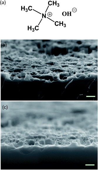
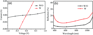
Fig. 1a shows the chemical structure of TMAH. The silanoles (Si–OH) groups on the Si substrate can be generated upon immersion in TMAH solution, which can be direct certified by the XPS measurement of Si (2p) peaks as shown in Fig. S2.† Fig. 1b shows the SEM images the SiNWs with TMAH treatment, it can be found that with TMAH treatment most bulk of the nanowires are etched, leaving the coarser root in the substrate. The increased space between SiNWs as well as the Si–OH groups formed in Si substrate is beneficial for the aqueous PEDOT:PSS infiltrating to SiNWs substrate. Thus comparing with the pristine one, as shown in Fig. 1c, the improved core–shell structure of the PEDOT:PSS/SiNWs is formed. In addition, as shown in Fig. S3,† the roughness of the rear Si substrate is reduced. Fig. 2a shows the current–voltage (J–V) curves between T-shaped Al pads at the rear side of the Si without (W/O) and with TMAH treatment. Here, Al pads are deposited by thermal evaporation at the rear side of the Si substrate as shown in the inset of Fig. 2a. It can be observed that the contact between Si and Al is non-ohmic when Al is directly deposited on Si, but with the TMAH treatment the contact between Si and Al is dramatically improved, enhancing the charge transfer/collection at the rear electrode.13,26 However, as shown in Fig. 2b, with the TMAH treatment, due to the decreased density and lengths of SiNWs, the light reflection of the SiNWs substrate with TMAH is higher than the pristine one.
Electrochemical impedance spectra (EIS) is an effective tool to reveal the effect of TMAH on the interfacial charge transfer/transport processes. Generally, from high to low frequency, three semicircles are observed in the Nyquist plots, representing the series resistance at the metal electrode (leftmost, Rs), the interfacial resistance of SiNWs/PEDOT:PSS (middle, R1) and the bulk resistance of the SiNWs (rightmost, R2), respectively.27,28 However, the middle one often overlaps with the high-frequency peak because of quite small series resistance of metal electrode. The equivalent circuit by Autolab software (inset) in Fig. 3 is further used to fit the experimental data of typical samples. For the device without TMAH treatment, the values of R1 and R2 are 4290 and 314 Ω, respectively. However, for the TMAH treatment device, due to the improve PEDOT:PSS and SiNWs contact area, the R1 enhances to 8975 Ω, while the R2 decreases to 275 Ω caused by the etched SiNWs substrate. Both of the values suggest that the electrochemical contact between Si and PEDOT:PSS is efficiently improved.
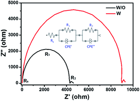 | ||
| Fig. 3 Nyquist plots of EIS spectra measured for devices without (W/O) and with (W) TMAH treatment at −0.5 V in the dark. The inset is the equivalent circuit used to fit the impedance spectra. | ||
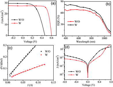
Fig. 4a shows the J–V curves of the PEDOT:PSS/SiNWs solar cells without and with TMAH treatment under simulated AM 1.5 illumination at 100 mW cm−2. The values of the open-circuit voltage (Voc), the short-circuit current density (Jsc), the fill factor (FF) and the PCE of the hybrid solar cells without and with TMAH treatment are summarized in Table 1. It can be seen that comparing with the pristine one, the Jsc of the hybrid solar cell with TMAH treatment has slight decreased from 29.22 to 27.32 mA cm−2, which is consistent with the integrated current values from the EQE spectra as shown in Fig. 4b. However, the corresponding Voc and FF of are obviously improved, from 0.470 to 0.598 V and 0.530 to 0.757, respectively. As a result, a PCE of 12.36% is achieved for the champion solar cell with TMAH treatment, which is 69.5% enhancement than the pristine one. Fig. S4† shows the UPS analysis of silicon substrate without and with TMAH treatment, it can be found that there is almost no change in the valance band as well as the work function of the silicon substrate after the TMAH treatment. Therefore, we conclude that the higher Voc achieved in the device with TMAH treatment can be mainly attributed to the decreased SiNWs surface area as well as the improved contact between the SiNWs and PEDOT:PSS. It is known that reducing the recombination velocity can greatly enhance the Voc of the devices.3,29,30 Since there are a large number of trap states on the Si surface, decreasing the SiNWs surface area can reduce the recombination velocity of the devices. Meanwhile, enhancing the contact between the SiNWs and PEDOT:PSS is beneficial for the charge transfer/collection, further reducing the recombination velocity of the device. As a result, the Voc of the device with TMAH is obviously enhanced. Fig. 4c shows the plot of dV/d(ln![[thin space (1/6-em)]](https://www.rsc.org/images/entities/char_2009.gif) J) versus J of the hybrid solar cells without and with TMAH treatment. The series resistance (Rs) of solar cells can be derived from the slope of dV/d(ln
J) versus J of the hybrid solar cells without and with TMAH treatment. The series resistance (Rs) of solar cells can be derived from the slope of dV/d(ln![[thin space (1/6-em)]](https://www.rsc.org/images/entities/char_2009.gif) J) versus J lines.13,26,31,32 It can be observed that after the TMAH treatment, due to the reduced charge recombination velocity, the charge recombination of the device is suppressed and charge transfer/collection efficiency is enhanced, therefore, the Rs of the device with the TMAH treatment decreases from 3.40 to 1.24 Ω cm2 for better charge transfer. Owing to the enhanced charge transfer/collection efficiency caused by the decreased SiNWs surface as well as the improved electrochemical contact between Si and PEDOT:PSS, the FF of the hybrid solar cell with TMAH is also improved. Notably, the enhanced rear contact in Fig. 2a also contributes to the higher FF and lower Rs.13,31
J) versus J lines.13,26,31,32 It can be observed that after the TMAH treatment, due to the reduced charge recombination velocity, the charge recombination of the device is suppressed and charge transfer/collection efficiency is enhanced, therefore, the Rs of the device with the TMAH treatment decreases from 3.40 to 1.24 Ω cm2 for better charge transfer. Owing to the enhanced charge transfer/collection efficiency caused by the decreased SiNWs surface as well as the improved electrochemical contact between Si and PEDOT:PSS, the FF of the hybrid solar cell with TMAH is also improved. Notably, the enhanced rear contact in Fig. 2a also contributes to the higher FF and lower Rs.13,31
| Device | Jsc (mA cm−2) | Voc (mV) | FF | PCE (%) |
|---|---|---|---|---|
| W/O | 29.22 | 470 | 0.530 | 7.28 |
| W | 27.32 | 598 | 0.757 | 12.36 |
In order to further confirm the suppression of the charge recombination for PEDOT:PSS/SiNWs devices with TMAH treatment, the minority carrier lifetime of the devices are measured. Fig. 5 depicts the spatial mapping of the effective minority carrier lifetime for the devices without and with TMAH treatment. Generally, the effective minority carrier lifetime of a silicon solar cell can be expressed as follow:7,14
| 1/teff = 1/tbulk + 2S/W | (1) |
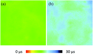 | ||
| Fig. 5 The minority carrier lifetime of the PEDOT:PSS/SiNWs hybrid solar cells without and with TMAH treatment. | ||
PEDOT:PSS/Si solar cell is generally assumed to be a Schottky junction solar cell, and the dark J–V curve can exhibit its rectifying characteristics and demonstrate that where the SiNWs/PEDOT:PSS heterojunction behave as well-defined diodes. Fig. 4d shows the J–V characteristics of the hybrid solar cells without and with TMAH treatment in dark circumstance. With the help of the thermionic emission model as follows:2,14
 | (2) |
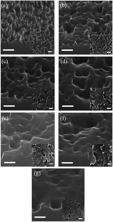
The etching time of TMAH plays an import role in the device performance. As the above discussion, with the TMAH treatment the contact between the SiNWs and PEDOT:PSS is improved, but the light harvest ability of the device is decreased. To optimize the etching time, the devices with different etching time are fabricated. In Fig. 7, the performance parameters of the PEDOT:PSS/SiNWs solar cells (Jsc, Voc, FF, and PCE) are plotted as functions of the etching time. Interestingly, it can be found that the Jsc in the PEDOT:PSS/SiNWs devices has a large drop at the first 15 s, and then has slight increase from 15 to 60 s. It is known that the reflection of the device is an important factor for the Jsc. As shown in Fig. S6,† the reflection of the device is increased along with the TMAH treatment time, thus the Jsc of the devices with TMAH treatment is lower than that of the device without treatment, decreasing at the first 15 s. Nevertheless, increasing the treatment time, the contact between the PEDOT:PSS layer and SiNWs substrate is enhanced, which is beneficial for the charge separation and collection. Therefore, though the reflection of the device is increased, the Jsc of the device has slight increased. Meanwhile, one can also observed that due to the improved the electrochemical contact between the PEDOT:PSS and SiNWs, as the etching time increase from 0 to 60 s, the FF increases from 0.530 to 0.757, and the Voc increase from 0.470 to 0.598 V. Thus, the PCE increases from 7.29% to 12.36%. Further increasing the etching time, all the performance parameters of the device decrease. In order to understand the reasons for the decrease of device performance, the SEM images of the SiNWs with different TMAH treatment time are further represented in Fig. 6. It can be seen that along with the TMAH treatment, the density as well as length of the SiNWs are reduced, the electrochemical contact between the PEDOT:PSS is also improved. However, the reflection of the SiNWs substrate is also increased (Fig. S6†). In addition, as shown in Fig. 7, with longer etching time, all of SiNWs are nearly etched, leaving the rougher Si substrate with small holes. Due to aqueous solution capillarity force of PEDOT:PSS, it is also hard for PEDOT:PSS to penetrate into the holes, leading the inferior performance of the device. Thus, the optimized etching time of SiNWs for TMAH is 60 s.
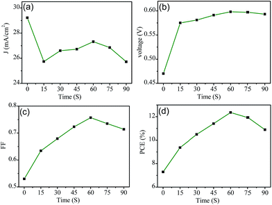 | ||
| Fig. 6 Jsc, Voc, FF, and PCE of the PEDOT:PSS/SiNWs hybrid solar cells are plotted as functions of the treatment time of TMAH. | ||
4. Conclusions
In summary, we have fabricated a series of PEDOT:PSS/Si hybrid solar cells based on the SiNWs substrate treated by TMAH. The SEM image, J–V curves and the minority carrier lifetime demonstrate that with the TMAH treatment, the density of the SiNWs is reduced, and the electrochemical contact between the PEDOT:PSS and SiNWs interface as well as the rear contact is greatly improved, all of which are significantly suppressing the charge recombination in the hybrid solar cells. The optimized treatment time of TMAH is also investigated which is 60 s. With longer treatment time, beside the lower light harvest absorption, the contact between Si and PEDOT:PSS is also decreased, resulting in the inferior performance of the devices. The resultant PCE of the hybrid solar cell can achieve up to 12.36%, which is 69.5% higher than that of pristine one. These preliminary results emphasize the importance of the TMAH treatment application in nanostructured Si and render a promising approach to obtain low-cost and high performance conjugated polymer/Si hybrid solar cells.Acknowledgements
This work was supported by National Natural Science Foundation of China (51402128, 21504061), the Natural Science Foundation of Jiangsu Province, China (No. BK20140561, BK20140311), University Science Research Project of Jiangsu Province (No. 13KJB150033) and a Project Funded by Jiangsu University for Senior Intellectuals (No. 13JDG101).Notes and references
- S.-C. Shiu, J.-J. Chao, S.-C. Hung, C.-L. Yeh and C.-F. Lin, Chem. Mater., 2010, 22, 3108–3113 CrossRef CAS
.
- S. Avasthi, S. Lee, Y. L. Loo and J. C. Sturm, Adv. Mater., 2011, 23, 5762–5766 CrossRef CAS PubMed
.
- X. Shen, B. Sun, D. Liu and S.-T. Lee, J. Am. Chem. Soc., 2011, 133, 19408–19415 CrossRef CAS PubMed
.
- T.-G. Chen, B.-Y. Huang, E.-C. Chen, P. Yu and H.-F. Meng, Appl. Phys. Lett., 2012, 101, 033301 CrossRef
.
- L. He, C. Jiang, H. Wang and D. Lai, ACS Appl. Mater. Interfaces, 2012, 4, 1704–1708 CAS
.
- J. P. Thomas and K. T. Leung, Adv. Funct. Mater., 2014, 24, 4978–4985 CrossRef CAS
.
- P. Yu, C.-Y. Tsai, J.-K. Chang, C.-C. Lai, P.-H. Chen, Y.-C. Lai, P.-T. Tsai, M.-C. Li, H.-T. Pan and Y.-Y. Huang, ACS Nano, 2013, 7, 10780–10787 CrossRef CAS PubMed
.
- F. Zhang, T. Song and B. Sun, Nanotechnology, 2012, 23, 194006 CrossRef PubMed
.
- Y. Jiang, X. Gong, R. Qin, H. Liu, C. Xia and H. Ma, Nanoscale Res. Lett., 2016, 11, 1–7 CrossRef CAS PubMed
.
- F. Zhang, B. Sun, T. Song, X. Zhu and S. Lee, Chem. Mater., 2011, 23, 2084–2090 CrossRef CAS
.
- J. S. Luo, A. H. Jensen, N. R. Brooks, J. Sniekers, M. Knipper, D. Aili, Q. F. Li, B. Vanroy, M. Wubbenhorst, F. Yan, L. V. Meervelt, Z. G. Shao, J. H. Fang, Z. H. Luo, D. E. De Vos and J. Fransaer, Energy Environ. Sci., 2015, 8, 1276–1291 CAS
.
- C.-Y. Liu, Z. C. Holman and U. R. Kortshagen, Nano Lett., 2008, 9, 449–452 CrossRef PubMed
.
- Y. Zhang, W. Cui, Y. Zhu, F. Zu, L. Liao, S.-T. Lee and B. Sun, Energy Environ. Sci., 2015, 8, 297–302 CAS
.
- X. Mu, X. Yu, D. Xu, X. Shen, Z. Xia, H. He, H. Zhu, J. Xie, B. Sun and D. Yang, Nano Energy, 2015, 16, 54–61 CrossRef CAS
.
- R. Liu, S. T. Lee and B. Sun, Adv. Mater., 2014, 26, 6007–6012 CrossRef CAS PubMed
.
- S. Kirchmeyer and K. Reuter, J. Mater. Chem., 2005, 15, 2077–2088 RSC
.
- M. Turbiez, P. Frère, M. Allain, C. Videlot, J. Ackermann and J. Roncali, Chemistry, 2005, 11, 3742–3752 CrossRef CAS PubMed
.
- W. Lu, C. Wang, W. Yue and L. Chen, Nanoscale, 2011, 3, 3631–3634 RSC
.
- E. C. Garnett and P. Yang, J. Am. Chem. Soc., 2008, 130, 9224–9225 CrossRef CAS PubMed
.
- K. Peng, Y. Xu, Y. Wu, Y. Yan, S. T. Lee and Z. Jing, Small, 2005, 1, 1062–1067 CrossRef CAS PubMed
.
- K. Q. Peng, J. J. Hu, Y. J. Yan, Y. Wu, H. Fang, Y. Xu, S. T. Lee and J. Zhu, Adv. Funct. Mater., 2006, 16, 387–394 CrossRef CAS
.
- K. Peng, W. Yin, F. Hui, X. Zhong, X. Ying and Z. Jing, Angew. Chem., 2005, 44, 2737–2742 CrossRef CAS PubMed
.
- O. Tabata, R. Asahi, H. Funabashi, K. Shimaoka and S. Sugiyama, Sens. Mater., 1992, 34, 51–57 CAS
.
- P. Papet, O. Nichiporuk, A. Kaminski, Y. Rozier, J. Kraiem, J. F. Lelievre, A. Chaumartin, A. Fave and M. Lemiti, Sol. Energy Mater. Sol. Cells, 2006, 90, 2319–2328 CrossRef CAS
.
- L. Wang, F. Wang, X. Zhang, N. Wang, Y. Jiang, Q. Hao and Y. Zhao, J. Power Sources, 2014, 268, 619–624 CrossRef CAS
.
- Y. Zhang, R. Liu, S.-T. Lee and B. Sun, Appl. Phys. Lett., 2014, 104, 083514 CrossRef
.
- X. Shen, L. Chen, J. Li and J. Zhao, J. Power Sources, 2016, 318, 146–153 CrossRef CAS
.
- X. Q. Bao and L. F. Liu, Mater. Chem. Phys., 2014, 149–150, 309–316 Search PubMed
.
- X. Shen, B. Sun, F. Yan, J. Zhao, F. Zhang, S. Wang, X. Zhu and S. Lee, ACS Nano, 2010, 4, 5869–5876 CrossRef CAS PubMed
.
- Z. Xia, T. Song, J. Sun, S.-T. Lee and B. Sun, Appl. Phys. Lett., 2014, 105, 241110 CrossRef
.
- Y. Zhang, F. Zu, S. T. Lee, L. Liao, N. Zhao and B. Sun, Adv. Energy Mater., 2014, 4, 201300923 Search PubMed
.
- X. Miao, S. Tongay, M. K. Petterson, K. Berke, A. G. Rinzler, B. R. Appleton and A. F. Hebard, Nano Lett., 2012, 12, 2745–2750 CrossRef CAS PubMed
.
- J. H. Werner, Appl. Phys. A, 1988, 47, 291–300 CrossRef
.
- D. Liu, Y. Zhang, X. Fang, F. Zhang, T. Song and B. Sun, IEEE Electron Device Lett., 2013, 34, 345–347 CrossRef CAS
.
Footnote |
| † Electronic supplementary information (ESI) available. See DOI: 10.1039/c6ra24970a |
| This journal is © The Royal Society of Chemistry 2017 |

