 Open Access Article
Enhanced electrochemical oxidation of phenol by boron-doped diamond nanowire electrode
Choong-Hyun Leea,
Eung-Seok Leea,
Young-Kyun Lima,
Kang-Hee Parkb,
Hee-Deung Parkb and
Dae-Soon Lim *a
*a
aDepartment of Materials Science and Engineering, Korea University, Seoul 02841, Republic of Korea. E-mail: dslim@korea.ac.kr; Fax: +82-2-928-3584; Tel: +82-2-3290-3272
bSchool of Civil, Environmental and Architectural Engineering, Korea University, Seoul 02841, Republic of Korea. E-mail: heedeung@korea.ac.kr; Fax: +82-2-928-7656; Tel: +82-2-3290-4861
First published on 18th January 2017
Abstract
We fabricated a boron-doped diamond nanowire (BDDNW) electrode via metal-assisted chemical etching (MACE) of Si and electrostatic self-assembly of nanodiamond (ESAND) seeding to provide a large surface area during the electrochemical oxidation process. The effect of nanostructuring of the BDD surface on the electrochemical oxidation performance and the current efficiency of the electrode in phenol were examined. Uniformly covered BDD on nanotextured Si substantially enhanced the electrochemical activity of the electrode. The effective surface area calculated from cyclic voltammetry (CV) was enhanced several times compared to that of a conventional planar BDD electrode. The BDDNW electrode also exhibited greatly enhanced chemical oxygen demand (COD), total organic carbon (TOC) removal behavior, and current efficiency. Furthermore, because of its excellent oxidation performance, the BDDNW electrode also exhibited much lower energy consumption in the phenol oxidation process.
1. Introduction
Large amounts of industrial wastewater containing toxic and nondegradable organic compounds have recently been discharged into the aquatic environment. For effective remediation of these effluents, some researchers have suggested the use of advanced oxidation processes (AOPs) that mainly utilize hydroxyl radicals (˙OH), which are highly oxidative agents.1 Exploiting the powerful oxidation ability of ˙OH (E0 = 2.80 V), AOPs can nonselectively react and mineralize organic compounds such as phenols, dyes, pharmaceuticals, herbicides and surfactants.2–5 Various AOP methods such as the Fenton process, ozonation, photocatalysis, ultrasound and electrochemical oxidation treatments are available for producing ˙OH.6–10 Electrochemical oxidation process are considered the most promising treatment method because of their high efficiency, wide applicability and environmental compatibility.11,12In an electrochemical oxidation process, various factors such as the applied current density, electrolytes, pH, operating temperature, initial organic concentration and electrode material can affect oxidation performance.13,14 The oxidation efficiency of an organic pollutant during treatment shows an especially strong dependence on the anode material because ˙OH are directly produced on the surfaces of the anode as a consequence of electrochemical water electrolysis.11 Several candidates for the anode material, including Pt, IrO2, SnO2, PbO2, glassy carbon (GC) and boron-doped diamond (BDD), have been investigated.15–18 Among these, BDD has been widely accepted as the most powerful anode material because of to its extremely high overpotential for the oxygen evolution reaction (OER).11,19,20 Additionally, BDD exhibits weak adsorption characteristics and tends to be chemically inert; consequently, numerous electrochemical wastewater treatment studies have been conducted on various organic oxidation mechanisms involving BDD anodes.21–23
Although BDD exhibits outstanding electro-oxidation performance, its utilization has thus far been limited to laboratory-scale experiments; its high cost makes it impractical in real wastewater treatment applications. To increase BDD electrode productivity and to overcome the drawback of its high cost, extensive effort has been directed toward achieving improved performance through modification of the conventional BDD electrode. The effect of the boron doping concentration of BDD on the oxidation of an aromatic compound has been studied by Bogdanowicz et al.24 A higher boron doping level of BDD was observed to lead to changes in diamond crystallites and in the density of the active sites on the surface, resulting in better oxidation performance. The influence of surface termination of BDD electrodes on organic oxidation has been investigated in several studies.25,26 The O-terminated BDD surface obtained via anodic polarization exhibits increased hydrophilicity, resulting in enhanced oxidation power of the anode. Souza et al. investigated the mineralization efficiency of 2,4-dichlorophenoxyacetic acid with respect to the sp3/sp2 ratio in BDD electrodes.27 They demonstrated that a higher content of sp3 diamond leads to more rapid oxidation.
Because the quantity of the produced ˙OH and its mobility mainly depend on the anode material, the surface area of the electrode is a critical factor in determining its oxidation performance. Although many reviews and research articles emphasize the effects of a large surface area of electrodes, only a few studies have focused on the BDD electrode surface area.28–30 He et al. fabricated a porous BDD electrode using a porous Ti substrate and demonstrated its electrochemical oxidation treatment performance. BDD pores with dimensions on the order of several tens of micrometers provided a large effective surface area and promoted current efficiency in the decomposition of various organic compounds. Nevertheless, fabrication of BDD on a Ti substrate requires long cooling time at the end of the CVD process because of the large thermal expansion gap and because of the problem of poorer long-term stability compared to that of Si-based BDDs, which results in delamination of the diamond film from the substrate due to residual stress.7,31 Moreover, the porous BDD of He et al. is limited to microsized structures, leaving the corresponding nanostructures, which are expected to exhibit substantially greater surface areas, unexplored.
To date, Si-based BDD nanostructures have been fabricated using various methods, including reactive-ion etching (RIE) of diamond, metal-assisted chemical etching (MACE) of Si, fabrication of carbon nanotube (CNT)–diamond hybrid structures and carbon dioxide activation.32–37 However, even though many techniques related to the nanostructuring of the BDD surface have been reported, these structures have only been applied in electrochemical sensor applications, not in electrochemical wastewater treatment processes.
In previous work, we examined the effect of micro-scaled texturing of BDD surface on dye (methyl orange) oxidation.38 In this work, we demonstrate the electrochemical phenol oxidation performance of nanostructured BDD electrodes fabricated by a simple etching treatment of Si substrates. We achieved a substantially greater surface area of BDD using the MACE process and electrostatic self-assembly of nanodiamond (ESAND) seeding. Nanocrystalline BDDs were deposited onto a substrate with a nanotextured Si surface morphology. BDD nanowires (BDDNWs) were thereby formed, providing a much larger surface area than the microstructure electrode examined in our previous work.38 We compared the electrochemical oxidation performance of the BDD nanowire and of the conventional planar BDD by examining the cyclic voltammetry (CV), chemical oxygen demand (COD), total organic carbon (TOC) and energy consumption of these two electrode materials in the oxidation of phenol.
2. Experimental procedure
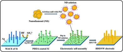
A p-type Si (100) wafer with 0.005 Ω cm resistivity was used as the substrate. The Si substrate was cleaned ultrasonically with ethanol and deionized water and subsequently immersed in 1% HF solution for 30 min. For Si surface nanotexturing, the MACE process was conducted in a solution of 4.5 M HF and 0.01 M AgNO3.39 Prior to chemical etching, the Si substrate was immersed in Piranha solution for 1 h to provide a hydrophilic surface. The surface-treated Si substrate was dipped into an etching solution for 5 min at 50 °C and then into a 30% HNO3 solution to remove residual silver dendrites.To provide a diamond nucleation site, we seeded nanodiamonds onto the Si substrate using the ESAND seeding technique. The conventional planar Si and nanotextured Si substrate were coated with poly(diallyldimethylammonium chloride) (PDDA) to provide a positively charged surface. The negatively charged nanodiamond particles in a poly(sodium 4-styrene sulfonate) (PSS) and nanodiamonds conjugate solution were electrostatically attached to the Si surfaces. Further information on the ESAND seeding method is provided in our previous report.40 After nanodiamond seeding, the planar BDD and BDDNW electrodes were synthesized by using hot-filament chemical vapor deposition (HFCVD) at a substrate temperature of 800 °C for 4 h. As the carbon source, 1 vol% of CH4 in H2 was fed at a total flow rate of 100 sccm; the diluted B2H6 gas concentration was maintained at [B]/[C] ratio of 5000 ppm in both electrodes. The total chamber pressure was maintained at less than 10 kPa. The BDDNW fabrication processes, including the nanodiamond seeding process, are depicted in Fig. 1.
After deposition, the microstructures and electrochemical properties of the BDD nanowire electrode were analyzed. Field-emission scanning electron microscopy (FESEM, Hitachi S-4300) was used to examine the surface morphology. For Raman spectra analysis, Raman spectroscopy with a 514.5 nm Ar-ion laser was used A potentiostat (Princeton Applied Research, VersaSTAT3) with a three-electrode cell of platinum, Ag/AgCl and a BDD nanowire electrode, representing the counter, reference and working electrodes, respectively, was used for electrochemical analyses.
˙OH produced by electrodes was determined by DNPH (2,4-dinitrophenylhydrazine) probe.41 Constant current density of 30 mA cm2 was applied in 0.5 M Na2SO4 solution with 5 mM methanol for 10 min. Formaldehyde was produced by reacting with methanol and transformed to a formaldehyde derivative by 20 mM DNPH (200 μL) with 1 M HCl (50 μL). Formaldehyde derivative was measured by Agilent 1260 high-performance liquid chromatography (HPLC) with UV absorbance at 360 nm.
To evaluate the bulk oxidation performance of the electrode, we constructed a single-compartment electrolytic circulation cell that operates in galvanostatic mode. The BDD nanowire electrode and a stainless steel plate were used as the anode and the cathode, respectively; the area of both electrodes was 4 × 4 cm2. The target organic compound was 1.0 mM phenol in 0.5 M Na2SO4 electrolyte (500 mL). The current density was fixed at 30 mA cm−2, and the total flow rate was 1 L min−1. During the 5 hours electrolysis, 2 mL of samples were extracted. After electrolysis, the COD (Hach DR-5000), the TOC (Shimadzu TOC-V CPH) and the phenol concentration (HPLC) were determined.
3. Results and discussion
We fabricated conventional planar BDD and BDDNW electrodes via the ESAND seeding and HFCVD techniques. Fig. 2(a)–(d) shows the surface and cross-sectional microstructures of the electrodes. Diamond crystals with a size of a few hundred nanometers were formed on planar Si, without forming pinholes. The thickness of the diamond layer in the planar BDD was approximately 200 nm. In the case of the BDDNW electrode, nanocrystalline BDDs grew well along the etched Si surfaces; the average length and thickness of the BDD nanowires were 200 nm and 750 nm, respectively. The ESAND method has been previously demonstrated to enable dense nanodiamond seeding on a complex nanotextured Si substrate without physical damage.36,38 Even though the planar BDD and BDDNW samples were fabricated under the same growth conditions, BDDNW exhibited a relatively lower growth rate, as indicated by its smaller crystal size and smaller film thickness. In Raman spectroscopy, both of planar BDD and BDDNW showed intense and clear nanocrystalline diamond peaks around 1130 cm−1.42 BDDNW showed slightly lower 1332 cm−1 band which attributed to the sp3 crystalline diamond phase and larger G peak (1550 cm−1) which attributed to the sp2 amorphous carbon.43,44 The peaks at 1430 and 1470 cm−1 are related with transpolyacetylene at grain boundaries which are typically observed in synthetic diamond film.45 Even though crystalline sp3 diamond phase portion was decreased, a larger crystal population and additional grain boundaries via surface nanostructuring of BDD would enhance its electrochemical properties, as measured on the basis of its electro-oxidation performance.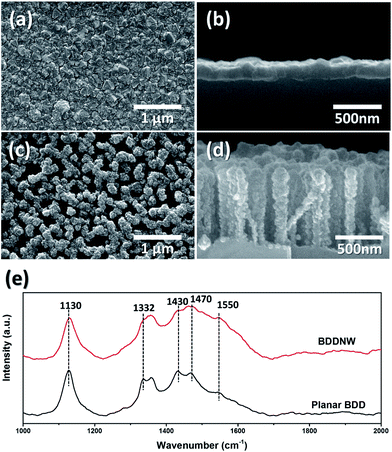 | ||
| Fig. 2 (a) SEM image of top view of planar BDD, (b) side view of planar BDD, (c) top view of BDDNW, (d) side view of BDDNW and (e) Raman spectras of electrodes. | ||
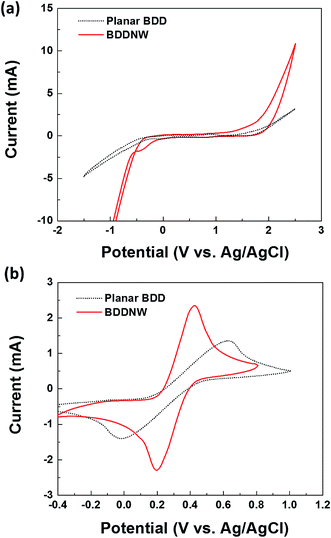
Fig. 3 shows the electrochemical properties of the planar BDD and BDDNW electrodes. Cyclic voltammograms obtained at a scan rate of 50 mV s−1 in 0.5 M H2SO4 are shown in Fig. 3(a). Both planar and BDDNW electrodes exhibit the wide working potentials (∼2.3 V) and high OER potentials typically observed for BDD electrodes. The OER potential is important in the electro-oxidation process because the ˙OH evolution reaction and the OER are competitive reactions. A higher OER potential restrains the oxygen evolution from water electrolysis and produces more ˙OH on the surface of the anode. Therefore, BDD exhibits a substantially higher electro-oxidation power than other electrodes.46,47 The current density of the BDDNW electrode is greater than that of the planar BDD electrode because of the BDDNWs' greater surface area; consequently, the BDDNW electrode should exhibit excellent electrochemical activity toward organic compounds. Increased surface area is also observed in the cyclic voltammograms for the Fe(CN)63−/4− redox couple, as shown in Fig. 3(b). In the case of the planar BDD, the anodic peak current (Ip,a) and the cathodic peak current (Ip,c) were 1.28 mA and −1.27 mA, respectively. The peak-to-peak separation potential (ΔEp) was 0.62 V. However, the BDDNW electrode shows significantly enhanced Ip,a (2.63 mA) and Ip,c (−2.38 mA) values and a significantly reduced ΔEp value (0.22 V). The lower ΔEp suggests that the electron transfer kinetics and the electrochemical activity of BDDNW are much better than those of the planar BDD electrode.48 Additionally, higher peak currents (Ip) indicate a larger effective surface area because the increase of Ip is proportional to the effective surface area. Fig. 4(a) shows variation of Ip with respect to the square root of the scan rate (v1/2) for the electrodes. Both peak currents show linear relationships, implying quasi-reversible behavior. Under this condition, the effective surface area is proportional to Ip/v1/2, as shown in the following equation:
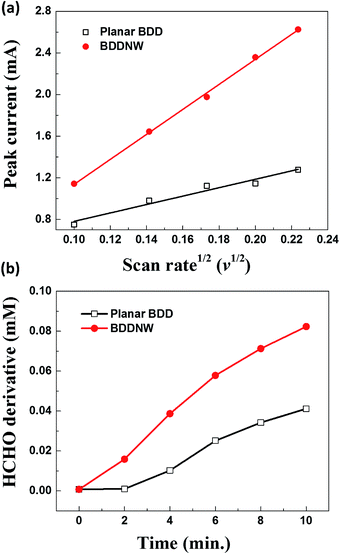 | ||
| Fig. 4 (a) Peak current versus the square root of the scan rate and (b) formaldehyde produced by reacting ˙OH with methanol. | ||
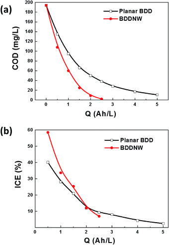
To evaluate the electro-oxidation performance, we conducted bulk electrolysis of 1 mM phenol using a single-compartment electrolytic cell with parallel electrodes. Fig. 5 shows a decrease of the COD and the instantaneous current efficiency (ICE) as a function of specific charge amount on the planar BDD and BDDNW electrodes. The ICE for the anodic oxidation of phenol was calculated using the following equation:
Fig. 6 shows the TOC, phenol removal and the mineralization efficiency (MCE). The MCE was calculated according to the equation:
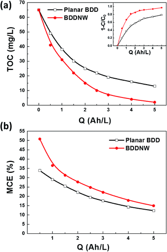 | ||
| Fig. 6 (a) TOC, phenol removal (inset) and (b) MCE curves for phenol oxidation on different electrodes. | ||
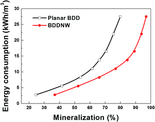
Fig. 7 shows specific energy consumption plotted with respect to phenol mineralization. The difference in the required specific energy increases dramatically with increasing the desired phenol mineralization. According to an extrapolation of the data, 27.5 kW h m−3 is required for 80% mineralization of phenol using the planar BDD electrode, whereas only 12.1 kW h m−3 is required using the BDDNW electrode. These results suggest that electrochemical oxidation of phenol using the BDDNW electrode is much more efficient from the standpoint of the economics of the oxidation process.
4. Conclusions
By using a metal-catalyzed silicon etching process and electrostatic nanodiamond seeding method, we successfully fabricated a BDDNW electrode for electrochemical oxidation processes. The BDDNW electrode exhibited an effective surface area that was three times greater than that of the planar-type BDD electrode; it also exhibited much faster electro-oxidation kinetics. In bulk electrolysis of phenol-containing water, the BDDNW electrode showed much higher COD and TOC removal rates as well as a higher current efficiency. Because of the large effective surface area of the nanowires, the BDDNW electrode generated large amounts of ˙OH. Despite the mass transfer limitation, the BDDNW electrode exhibited highly improved electrochemical oxidation performance compared to the microtextured BDD electrode investigated in our previous study as well as compared to other microstructured BDD electrodes. Additionally, nanostructuring of the BDD electrode reduced specific energy consumption for 80% mineralization of phenol by a factor of more than 2 compared to the conventional planar BDD electrode. These results indicate that because of the larger surface area of nanostructured BDD, nanostructuring of the BDD electrode may solve the problem associated with the high production cost per unit area of BDD electrodes and can potentially be applied in applications involving real wastewater.Acknowledgements
This work was supported by Korea Ministry of Environment (MOE) as “Public Technology Program based on Environmental Policy” (No. E416-00070-0604-0).References
- M. Cheng, G. M. Zeng, D. L. Huang, C. Lai, P. Xu, C. Zhang and Y. Liu, Chem. Eng. J., 2016, 284, 582–598 CrossRef CAS.
- J. Hoigne, Water Sci. Technol., 1997, 35, 1–8 CrossRef CAS.
- M. Pera-Titus, V. Garcia-Molina, M. A. Banos, J. Gimenez and S. Esplugas, Appl. Catal., B, 2004, 47, 219–256 CrossRef CAS.
- S. W. da Silva, C. R. Klauck, M. A. Siqueira and A. M. Bernardes, J. Hazard. Mater., 2015, 282, 241–248 CrossRef CAS PubMed.
- A. R. F. Pipi, I. Sires, A. R. De Andrade and E. Brillas, Chemosphere, 2014, 109, 49–55 CrossRef CAS PubMed.
- K. Ikehata, N. J. Naghashkar and M. G. Ei-Din, Ozone: Sci. Eng., 2006, 28, 353–414 CrossRef CAS.
- Y. Tian, X. M. Chen, C. Shang and G. H. Chen, J. Electrochem. Soc., 2006, 153, J80–J85 CrossRef CAS.
- E. Brillas, I. Sires and M. A. Oturan, Chem. Rev., 2009, 109, 6570–6631 CrossRef CAS PubMed.
- Y. G. Adewuyi, Environ. Sci. Technol., 2005, 39, 8557–8570 CrossRef CAS PubMed.
- S. G. Kumar and K. S. R. K. Rao, RSC Adv., 2015, 5, 3306–3351 RSC.
- A. Kraft, M. Stadelmann and M. Blaschke, J. Hazard. Mater., 2003, 103, 247–261 CrossRef CAS PubMed.
- A. Sakalis, K. Fytianos, U. Nickel and A. Voulgaropoulos, Chem. Eng. J., 2006, 119, 127–133 CrossRef CAS.
- T. Bechtold, A. Turcanu and W. Schrott, Diamond Relat. Mater., 2006, 15, 1513–1519 CrossRef CAS.
- R. E. Palma-Goyes, F. L. Guzman-Duque, G. Penuela, I. Gonzalez, J. L. Nava and R. A. Torres-Palma, Chemosphere, 2010, 81, 26–32 CrossRef CAS PubMed.
- J. T. Xing, D. H. Chen, W. Zhao, X. L. Peng, Z. L. Bai, W. W. Zhang and X. X. Zhao, RSC Adv., 2015, 5, 53504–53513 RSC.
- S. P. Li, Y. H. Li, X. Y. Zeng, W. R. Wang, R. X. Shi and L. N. Ma, RSC Adv., 2015, 5, 68700–68713 RSC.
- Y. Wang, C. C. Shen, L. F. Li, H. Y. Li and M. M. Zhang, RSC Adv., 2016, 6, 30598–30610 RSC.
- A. Urtiaga, P. Fernandez-Castro, P. Gomez and I. Ortiz, Chem. Eng. J., 2014, 239, 341–350 CrossRef CAS.
- J. H. T. Luong, K. B. Male and J. D. Glennon, Analyst, 2009, 134, 1965–1979 RSC.
- W. Zhang, S. Y. Zhu, R. Luque, S. Han, L. Z. Hu and G. B. Xu, Chem. Soc. Rev., 2016, 45, 715–752 RSC.
- E. Brillas, B. Boye, I. Sires, J. A. Garrido, R. M. Rodriguez, C. Arias, P. L. Cabot and C. Comninellis, Electrochim. Acta, 2004, 49, 4487–4496 CrossRef CAS.
- F. Montilla, P. A. Michaud, E. Morallon, J. L. Vazquez and C. Comninellis, Electrochim. Acta, 2002, 47, 3509–3513 CrossRef CAS.
- P. Canizares, C. Saez, J. Lobato and M. A. Rodrigo, Ind. Eng. Chem. Res., 2004, 43, 6629–6637 CrossRef CAS.
- R. Bogdanowicz, A. Fabianska, L. Golunski, M. Sobaszek, M. Gnyba, J. Ryl, K. Darowicki, T. Ossowski, S. D. Janssens, K. Haenen and E. M. Siedlecka, Diamond Relat. Mater., 2013, 39, 82–88 CrossRef CAS.
- C. Chen, E. Nurhayati, Y. Juang and C. Huang, J. Environ. Sci., 2016, 45, 100–107 CrossRef PubMed.
- D. A. Tryk, H. Tachibana, H. Inoue and A. Fujishima, Diamond Relat. Mater., 2007, 16, 881–887 CrossRef CAS.
- F. L. Souz, C. Saez, M. R. V. Lanza, P. Canizares and M. A. Rodrigo, Electrochim. Acta, 2016, 187, 119–124 CrossRef.
- B. P. Chaplin, Environ. Sci.: Processes Impacts, 2014, 16, 1182–1203 CAS.
- A. Kraft, Int. J. Electrochem. Sci., 2007, 2, 355–385 CAS.
- M. Panizza, P. A. Michaud, G. Cerisola and C. Comninellis, Electrochem. Commun., 2001, 3, 336–339 CrossRef CAS.
- P. Y. Lim, F. Y. Lin, H. C. Shih, V. G. Ralchenko, V. P. Varnin, Y. V. Pleskov, S. F. Hsu, S. S. Chou and P. L. Hsu, Thin Solid Films, 2008, 516, 6125–6132 CrossRef CAS.
- Y. S. Zou, Y. Yang, Y. L. Zhou, Z. X. Li, H. Yang, B. He, I. Bello and W. J. Zhang, J. Nanosci. Nanotechnol., 2011, 11, 7914–7919 CrossRef CAS PubMed.
- N. J. Yang, H. Uetsuka and C. E. Nebel, Adv. Funct. Mater., 2009, 19, 887–893 CrossRef CAS.
- D. B. Luo, L. Z. Wu and J. F. Zhi, ACS Nano, 2009, 3, 2121–2128 CrossRef CAS PubMed.
- H. Zanin, P. W. May, D. J. Fermin, D. Plana, S. M. C. Vieira, W. I. Milne and E. J. Corat, ACS Appl. Mater. Interfaces, 2014, 6, 990–995 CAS.
- S. K. Lee, M. J. Song, J. H. Kim, T. S. Kan, Y. K. Lim, J. P. Ahn and D. S. Lim, NPG Asia Mater., 2014, 6, e115 CrossRef CAS.
- J. F. Zhang, T. Nakai, M. Uno, Y. Nishiki and W. Sugimoto, Carbon, 2014, 70, 207–214 CrossRef CAS.
- J. Y. Bak, C. H. Lee, J. D. Kim and D. S. Lim, J. Korean Phys. Soc., 2016, 68, 109–114 CrossRef CAS.
- K. Q. Peng, Z. P. Huang and J. Zhu, Adv. Mater., 2004, 16, 73–76 CrossRef CAS.
- J. H. Kim, S. K. Lee, O. M. Kwon and D. S. Lim, J. Nanosci. Nanotechnol., 2009, 9, 4121–4127 CrossRef CAS PubMed.
- C. Tai, J. F. Peng, J. F. Liu, G. B. Jiang and H. Zou, Anal. Chim. Acta, 2004, 527, 73–80 CrossRef CAS.
- K. Siuzdak, R. Bogdanowicz, M. Sawczak and M. Sobaszek, Nanoscale, 2015, 7, 551–558 RSC.
- J. V. Macpherson, Phys. Chem. Chem. Phys., 2015, 17, 2935–2949 RSC.
- P. W. May, W. J. Ludlow, M. Hannaway, P. J. Heard, J. A. Smith and K. N. Rosser, Chem. Phys. Lett., 2007, 446, 103–108 CrossRef CAS.
- S. Prawer and R. J. Nemanich, Philos. Trans. R. Soc., A, 2004, 362, 2537–2565 CrossRef CAS PubMed.
- M. Panizza and G. Cerisola, Electrochim. Acta, 2003, 48, 3491–3497 CrossRef CAS.
- M. Panizza and G. Cerisola, Electrochim. Acta, 2004, 49, 3221–3226 CrossRef CAS.
- X. H. Kang, J. Wang, H. Wu, I. A. Aksay, J. Liu and Y. H. Lin, Biosens. Bioelectron., 2009, 25, 901–905 CrossRef CAS PubMed.
- A. J. Bard and L. R. Faulkner, Electrochemical Methods: Fundamentals and Applications, Wiley, New York, 2000 Search PubMed.
- S. Trasatti and O. A. Petrii, J. Electroanal. Chem., 1992, 327, 353–376 CrossRef CAS.
- C. Comninellis and C. Pulgarin, J. Appl. Electrochem., 1991, 21, 703–708 CrossRef CAS.
- C. A. Martinez-Huitle and S. Ferro, Chem. Soc. Rev., 2006, 35, 1324–1340 RSC.
- Y. P. He, W. M. Huang, R. L. Chen, W. L. Zhang and H. B. Lin, Sep. Purif. Technol., 2015, 149, 124–131 CrossRef CAS.
- P. Canizares, J. Lobato, R. Paz, M. A. Rodrigo and C. Saez, Water Res., 2005, 39, 2687–2703 CrossRef CAS PubMed.
- C. Comninellis and A. Nerini, J. Appl. Electrochem., 1995, 25, 23–28 CrossRef CAS.
| This journal is © The Royal Society of Chemistry 2017 |

