 Open Access Article
Electrospray technique in fabricating perovskite-based hybrid solar cells under ambient conditions
Pei-Ying Lina,
Yueh-Ying Chenb,
Tzung-Fang Guo*ac,
Yaw-Shyan Fu *b,
Li-Chung Laid and
Chung-Kwang Leed
aDepartment of Photonics, National Cheng Kung University, 70101 Tainan, Taiwan, Republic of China. E-mail: guotf@mail.ncku.edu.tw
bDepartment of Greenergy, National University of Tainan, 70005 Tainan, Taiwan, Republic of China. E-mail: ysfu@mail.nutn.edu.tw
cAdvanced Optoelectronic Technology Center, National Cheng Kung University, 70101 Tainan, Taiwan, Republic of China
dGreen Technology Research Institute CPC Corporation, 81126 Kaohsiung, Taiwan, Republic of China
First published on 10th February 2017
Abstract
In this work, we utilized the electrospray technique to deposit the solidified crystal precursors on the substrate to investigate the transition processes in forming an orthorhombic methylammonium lead iodide film for fabricating perovskite planar heterojunction solar cells. The formation of solidified crystal precursors by the electrospray technique improves the de-wetting of the perovskite film on the substrate. Judicious selection of the applied voltage in the electrospray process generates crystal precursors of the appropriate dimensions. These as-electrosprayed crystals are the solid-state reactants for the halogen exchange and they form a uniformly covered film on the substrate under suitable annealing conditions. The hybrid device prepared by the electrospray technique exhibits a power conversion efficiency of 9.3%, a short-circuit current of 19.71 mA cm−2, an open-circuit voltage of 0.87 V, and a fill factor of 0.55. The electrospray technique with the solid-state reaction mechanism proposed in this paper would be ideal for the large-area coating of a perovskite active layer, and thus has potential for use in real mass production.
Introduction
The organic–inorganic hybrid organometal halide perovskites have drawn much attention due to their high absorption coefficients, direct band gaps, and long diffusion lengths.1–5 Miyasaka's group first employed methylammonium lead iodide (CH3NH3PbI3, MAPbI3) as a light sensitizer in dye-sensitized solar cells in 2009,6 and since then researchers have made many improvements to advance the photovoltaic parameters of perovskite-based hybrid solar cells. Snaith and co-workers used the mixed halide perovskite precursors CH3NH3PbI3−xClx deposited on “scaffold” Al2O3,7,8 and found that the perovskite layer may transport electrons without n-type TiO2. Etgar et al. reported the production of a conductor-free mesoscopic perovskite/TiO2 heterojunction solar cell.9 These studies indicated that the perovskite may function as a compound semiconductor to absorb the light and transport electrons/holes in the active layer. Based on this idea, various prototypes of planar architecture have been developed. An earlier work reported on the donor–acceptor contact interface for charge separation, based on the hybrid CH3NH3PbI3 perovskite/fullerene (C60) planar heterojunction (PHJ) with a device configuration of organic photovoltaics (OPVs).10 Current perovskite-based solar cells with a planar architecture have achieved a highest power conversion efficiency (PCE) of approximately 20%.11–13Our previous work successfully demonstrated the fabrication of efficient hybrid solar cells by the spin-coating technique to form a perovskite layer in the PHJ configuration.10 Many recent studies have reported processes to optimize device performance.14–20 Some two-step approaches apply the pre-coated PbI2 to the substrate followed by a reaction with CH3NH3I (MAI) vapor at 150 °C in N2 atmosphere,14 or an inter-diffusion reaction between MAI with PbI2 in a MAI/PbI2 double layer configuration15,16 to form the perovskite layer. Other approaches apply the mixed solvent to enhance the morphology of perovskite film17,18 or introduce the additives (1,8-diiodooctane, polyvinylpyrrolidone, NH4Cl or HI) into the precursor solution to improve the crystallinity while casting the perovskite layer.19,20 However, during the film forming process of the perovskite layer, the de-wetting of the film on the substrate causes supersaturation of the solution at different times and positions. In addition, the wet-coating approach may not be a suitable process to prepare the perovskite layer on a large-area substrate, which is needed for practical applications. Accordingly, we are interested in developing an approach to deposit solidified crystal precursors on the substrate at an early reaction stage and then to convert the solid precursors into a perovskite layer through a solid-state reaction at an elevated temperature, as this process could be suitable for large-area coating.
Solid state reactions have been applied to prepare light-absorbing layers, such as Cu2ZnSnS4 (CZTS)21 and CuInSe2 (CIS),22 under non-vacuum conditions. We fabricated a CuInSe2 thin film via a low temperature solid state reaction from the as-deposited individual binary precursor CuSe and InSe powders.23 It should be noted that nanocrystals are more chemically active than bulk materials in the solid-state reaction to convert the reactant into the product.24 The electrospray technique produces size-selected and highly dispersive nanocrystals,25–27 such as nanostructure oxide ceramic powders,28–30 for use in light emitting diodes,31 fuel cells32,33 and solar cells.34,35 In other words, the electrospray method could be a suitable and easy process to deposit small solidified crystals of the appropriate dimensions for halide exchange, thus enabling phase transformation in the solid-state reaction to prepare the perovskite active layer on the substrate.
In this paper, we apply an electrospray technique to make the solidified crystals that are then used as precursors. Later, through solid-state diffusion induced by heat treatment, the solid precursors convert to an orthorhombic CH3NH3PbI3 layer for the fabrication of hybrid perovskite/C60 PHJ solar cells. We adjust the applied voltages in the electrospray process to modulate the dispersion density of the solidified crystals, which is the key parameter to determining the surface coverage of the precursors for the subsequent solid reaction. The orthorhombic CH3NH3PbI3 perovskite film exhibits a suitable morphology for use in device fabrication. The resulting cell presents decent photovoltaic parameters, with an open-circuit voltage (VOC) of 0.87 V, a short-circuit current (JSC) of 19.71 mA cm−2, and a fill factor (FF) of 0.55, corresponding to a PCE of 9.3%. The electrospray technique with the solid reaction mechanism proposed in this paper would be ideal for the large-area coating of a perovskite layer for real mass production.
Experimental
Material and sample preparation
Methyl ammonium iodide (CH3NH3I) was synthesized by reacting 14 mL of methylamine (CH3NH2, 40 wt% in methanol, Alfa Aesar) and 15 mL of hydroiodic acid (HI, 57 wt% in water, Showa) in a 100 mL round-bottom flask at 0 °C under nitrogen atmosphere for 2 h with stirring. After the reaction, the solvent of the solution was evaporated using a rotary evaporator and the solvents were carefully removed at 50 °C. A white colored powder, CH3NH3I, was formed after the reaction. The precipitate was washed with diethyl ether (99.7%, Sigma-Aldrich) three times and dried at 60 °C in a vacuum oven overnight. Precursor solution CH3NH3PbI3−xClx was synthesized by mixing CH3NH3I and lead chloride (PbCl2) (98%, anhydrous, Merck) in a 3![[thin space (1/6-em)]](https://www.rsc.org/images/entities/char_2009.gif) :
:![[thin space (1/6-em)]](https://www.rsc.org/images/entities/char_2009.gif) 1 molar ratio with a total concentration of 100 mg mL−1 dissolved in N,N-dimethylformamide (DMF) (≥99.8%, Fisher Scientific) at 60 °C with stirring for 12 h.
1 molar ratio with a total concentration of 100 mg mL−1 dissolved in N,N-dimethylformamide (DMF) (≥99.8%, Fisher Scientific) at 60 °C with stirring for 12 h.
Device fabrication
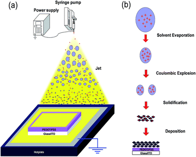
Prior to device fabrication, the pre-patterned glass/indium-tin-oxide (ITO) (15 Ω □−1, RITEK Corp.) was sequentially cleaned by ultrasonic treatment in detergent, de-ionized water, acetone and isopropyl alcohol. For the cell fabricated on a glass/ITO/poly(3,4-ethylenedioxythiophene) poly(styrene-sulfonate) (PEDOT:PSS) substrate, the PEDOT:PSS (Baytron PVP Al 4083, filtered with 0.45 μm PVDF filter) was spin-coated onto the ultraviolet ozone treated glass/ITO substrate at 4000 rpm for 60 s, and then annealed in air at 150 °C for 25 minutes. The perovskite precursor was then deposited on the glass/ITO/PEDOT:PSS under ambient conditions by electrospray deposition. The electrospray setup is depicted in Fig. 1(a), and consisted of a syringe and needle (internal diameter 0.21 mm), a syringe pump (KdScientific, Model 200), a high positive voltage power supply (You-Shang Technical Corp.), and an aluminium foil as the plate ground electrode. At the electrospray deposition, a syringe attached to a syringe pump was filled with the as-prepared CH3NH3PbI3−xClx solution. The flow rate was set at 0.5 mL h−1. The electrospray started by applying a high positive voltage of 20 kV at the electrode (nozzle head). The distance between the nozzle head and the ground electrode (aluminium foil) was 9 cm. The deposition time was 80 s, and the substrate was held at 70 °C by a hotplate. The perovskite films were then annealed at 90, 110, 130 °C for 60 minutes under ambient conditions. Afterward, the samples were transferred to a thermal evaporator to deposit the fullerene (C60) (30 nm) (>99.0%, Solenne), bathocuproine (BCP) (10 nm) (Sigma-Aldrich), and Al electrode (100 nm) in sequence under a vacuum of 6 × 10⁻⁶ Torr. The active area of the device was 0.06 cm2.Characterization
The device characteristics, the current density–voltage (J–V) curves, were measured in a nitrogen-filled glove box using a Keithley 2400 SourceMeter under standard 1 sun AM 1.5G simulated irradiation (100 mW cm−2) from a Newport 91160A 300W Solar Simulator (Class A). The light intensity for the illumination can be tuned by placing a neutral density filter in front of the device during the measurement. The scan rate was 0.1 V s−1. The simulated solar irradiance was corrected by a Schott visible-color glass-filtered (KG5 color filter) Si diode (Hamamatsu S1133). The incident photon to electron conversion efficiency (IPCE) spectra were measured by a 300 W xenon light source (Oriel), Oriel Cornerstone 130 1/8 m monochromator, Keithley 2400 sourcemeter, a chopper (SR540, Stanford Research System Inc.) and a Lock-in amplifier (SR510, Stanford Research System Inc.). The crystallographic properties of perovskite on the glass/ITO/PEDOT:PSS substrate were characterized by X-ray diffraction (XRD) measurements (Simatsu, XRD6000, Japan), as recorded using a Cu Kα (λ = 0.15418 nm) radiation source that was operated at 40 kV and 100 mA. The X-ray diffractogram was obtained at a scan rate of 0.03° s−1 for 2θ values between 10° and 60°. The surface coverage of the perovskite images was obtained using an optical microscope (Olympus BX51M, Japan) and analyzed using the ImageJ software package. The particle images were obtained using a scanning electron microscopy (SEM) system (Hitachi, 4200A, Japan) operating at 10 kV.Results and discussion
The solidified crystals were prepared on a glass/indium-tin-oxide (ITO)/poly(3,4-ethylenedioxythiophene) poly(styrene-sulfonate) (PEDOT:PSS) substrate by the electrospray technique described above. Since the electrostatic force overcomes the surface tension of the spray solution at a sufficiently high electric bias, the solution arriving at the nozzle head directly nebulizes as a jet of liquid droplets. Eventually, these droplets are accelerated by the electric field toward the grounded plate and deposited on the glass/ITO/PEDOT:PSS substrate.Fig. 1(b) shows a schematic of the formation of solidified crystals on the glass/ITO/PEDOT:PSS substrate. There are four steps that occur as the droplets are accelerated toward the grounded plate in the electrospray process: solvent evaporation, coulombic explosion, solidification and deposition. Liquid droplets in a jet carry charges when they leave the nozzle head. The droplets are dispersed due to the repulsive force of the charges on the droplets. “Solvent evaporation” then occurs and raises the surface charge density due to a decrease in the droplet volume and the surface area. As electrostatic force overcomes the surface tension to reach the limit of the charge-mass ratio (the Rayleigh limit36), the droplets further disrupt into smaller droplets (satellite droplets), a process which is termed “Coulombic explosions”. The droplets continuously go through the above “solvent evaporation” and “Coulombic explosions” processes several times while traveling between the nozzle head and substrate. Finally, the evaporation of solvent precipitates the solutes from the tiny droplets and the solidified solutes are deposited on the substrate. The deposition of the solidified crystals or powders is correlated with the tiny droplet sizes, which can be modulated by the applied voltage on the nozzle head and the distance from the substrate. Accordingly, the size-selected and highly dispersive nano solids can be deposited on the glass/ITO/PEDOT:PSS substrate by the electrospray process.
Fig. 2 shows the optical microscope (OM) images of the films on glass/ITO/PEDOT:PSS substrates as deposited by different applied voltages. The concentration of the electrospray solution, deposition time, and the substrate temperature were all identical and set at 100 mg L−1, 80 s, and 70 °C, respectively. As illustrated by the OM images in Fig. 2, the surface of the substrate for the samples deposited at the biased voltages between 9 to 14 kV is composed of many large patterns. Presumably, the electrostatic force at these biases did not reach the Rayleigh limit on the droplets to induce sequential coulombic explosions, so the droplet size did not decrease. The large droplets were thus directly deposited on the substrate, resulting in a very rough surface morphology of the films on the substrate. Further increasing the applied voltages to a magnitude of 15–22 kV markedly improved the coverage of the solid films on the substrates, as depicted in Fig. 2. It should be noted that the sample prepared using a 20 kV applied voltage is densely covered with a solid film, and this would thus be the optimal condition in this study. However, the high voltage, 22 kV, has a negative effect on the deposition of the film. As shown in Fig. 2, there are many dark patterns on the OM image of the sample deposited at 22 kV. At the high applied voltage the droplets easily explode at an early stage due to the fact that the Coulomb force is greater than the surface tension in the droplet,37 which can lead to non-uniform deposition of the solids on the substrate.
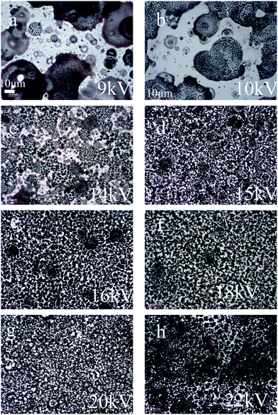 | ||
| Fig. 2 OM images of the films on glass/ITO/PEDOT:PSS substrates as deposited by different applied voltages: (a) 9, (b) 10, (c) 14, (d) 15, (e) 16, (f) 18, (g) 20, and (h) 22 kV. | ||
Fig. 3 shows the X-ray diffraction (XRD) patterns for the as-deposited film prepared at 20 kV on glass/ITO/PEDOT:PSS substrates and the films annealed at 110 °C for 0, 20 and 60 minutes. As shown in Fig. 3, the peaks at 14.1°, 28.4°, 43.2°, and 58.9° are assigned to the (110), (220), (330), and (440) planes, respectively, for the orthorhombic crystal structure of CH3NH3PbI3.38 For the as-deposited film without 110 °C annealing, the peaks at 12° and 16.8° (marked with “*” sign) are assigned to XRD patterns by a Pb-complex39,40 composed of Pb halide and the organic species. We observe a small shift in preferred orientation (220) peaks toward the higher diffraction angles with the d-spacing changes in Fig. 3(b), indicating lattice distortion by the substitution of the Cl with I as the atom radius of Cl (0.167 nm) atoms is much smaller than I (0.206 nm). The excess Cl ions in the solid film react with CH3NH3PbI3 crystallite and form a CH3NH3PbI3:Cl intermediate at early reaction stage. Through the thermal treatment to anneal the film at 110 °C for 20 minutes, the magnitudes of the (100) and (200) peaks increase markedly and the peaks at 12° and 16.8°, as shown in the XRD pattern of the as-deposited sample disappear, indicating the transformation of precursors to form orthorhombic CH3NH3PbI3. The prolonged thermal treatment (110 °C for 60 minutes) further increases the relative magnitude of XRD patterns, with a full width at half maximum (FWHM) of 0.22°, suggesting the relatively high crystallinity of perovskite film, and the peak at the 15.6° diffraction angle assigned to MAPbCl3 disappears, as shown in the inset of Fig. 3(b). This observation for the thermal treatment of orthorhombic CH3NH3PbI3 perovskite herein agrees with the results of previous research.41 In this study, annealing the film prepared by electrospraying at 110 °C for 60 minutes can form an orthorhombic CH3NH3PbI3 film on the glass/ITO/PEDOT:PSS substrate with the appropriate crystal phases for device fabrication.
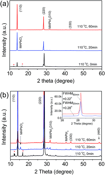 | ||
| Fig. 3 XRD patterns for the as-deposited film prepared at 20 kV on glass/ITO/PEDOT:PSS substrates and the films annealed at 110 °C for 0, 20 and 60 minutes. | ||
It should also be noted that surface morphology of the perovskite films produced in this study is correlated with the annealing temperature. Fig. 4 shows scanning electron microscopy (SEM) images with a magnification of 5k× for perovskite films on glass/ITP/PEDOT:PSS substrates annealed at 70, 90, 110, and 130 °C for 60 minutes. For the sample annealed at 70 °C, as presented in Fig. 4(a), the SEM image shows that the surface morphology is composed of many solid particles with dimensions of around 1.5–2.0 μm. This indicates that the temperature of 70 °C is too low to initiate the interdiffusion process of the solid to form a continuous film on the substrate. Fig. 4(b) presents an SEM image of the sample annealed at 90 °C for 60 minutes. Under this annealing condition, we observe the growth of perovskite film on the substrate as induced by the diffusion of the solid at the elevated temperature, but there are still many voids with dimensions larger than a few μm. The number and density of voids should thus be reduced for better coverage of the film on the substrate. Further increasing the temperature to 110 °C markedly improves the morphology of the perovskite film and decreases the surface roughness, as illustrated in Fig. 4(c). This result is correlated with XRD measurement in Fig. 3, which shows that the film exhibits a good crystal structure when annealed at 110 °C for 60 minutes. However, annealing the sample at 130 °C dramatically changes the surface morphology. As shown in Fig. 4(d), the SEM image reveals many large crystals on the substrate. The film is discrete, with many big voids between grains, and thus is not applicable as an active layer for the fabrication of good photovoltaic cells.
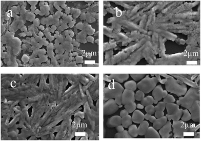 | ||
| Fig. 4 SEM images of the perovskite films on glass/ITP/PEDOT:PSS substrates annealed at (a) 70, (b) 90, (c) 110, and (d) 130 °C for 60 minutes. | ||
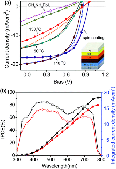
Fig. 5(a) presents the schematic device structure and the current density–voltage (J–V) curves with forward (hollow icons) and reverse scans (solid icons) of hybrid perovskite solar cells of glass/ITO/PEDOT:PSS/orthorhombic CH3NH3PbI3 perovskite/C60/bathocuproine (BCP)/Al configuration under the standard 1 sun AM 1.5G simulated solar irradiation. As plotted in Fig. 5, the hybrid cell made of a CH3NH3PbI3−xClx active layer by the electrospray method reported in this work exhibits a VOC of 0.87 V, a JSC of 19.71 mA cm−2, and an FF of 0.55, corresponding to a PCE of 9.3%. These photovoltaic parameters are comparable to those of a hybrid cell with a CH3NH3PbI3−xClx active layer prepared by the conventional spin-coating process, which exhibits a VOC of 0.94 V, a JSC of 17.74 mA cm−2, and an FF of 0.6, corresponding to a PCE of 10%. Fig. 5(b) shows the incident photon to electron conversion efficiency (IPCE) spectrum of the cell fabricated by electrospraying having a peak IPCE above 80% at approximately 420–500 nm. The photocurrent integrated from the overlap of the IPCE spectrum with the AM 1.5G solar irradiation gives a current density of 18.35 mA cm−2, in which the integrated photocurrent is correlated with a magnitude of JSC, as depicted in Fig. 5(a). Fig. 6 shows the cross-sectional image of the hybrid device in this study. We observe a compact perovskite active layer with a thickness of approximately 380–400 nm. The electrospray technique developed herein is thus a suitable approach to deposit perovskite materials for fabricating hybrid solar cells. For the devices made of an orthorhombic CH3NH3PbI3 active layer annealed at 90 °C and 130 °C instead of 110 °C for 60 minutes, we observe the photovoltaic parameters of a VOC of 0.81 V, a JSC of 15.23 mA cm−2, and an FF of 0.44, corresponding to a PCE of 5.4% for the 90 °C device, and a VOC of 0.85 V, a JSC of 13.57 mA cm−2, and an FF of 0.30, corresponding to a PCE of 3.5% for the 130 °C device. The relatively low device performance is due to the non-uniform coverage or incomplete reaction of perovskite film on the substrate. As seen in the SEM image in Fig. 4(d), the voids between grain boundaries cause electric shunting between the electrodes, markedly reducing the FF, JSC, and PCE of the solar cells. In addition, the J–V curve for the hybrid cell made of a CH3NH3PbI3 active layer prepared by electrospraying CH3NH3I and PbI2 (molar ratio of 1![[thin space (1/6-em)]](https://www.rsc.org/images/entities/char_2009.gif) :
:![[thin space (1/6-em)]](https://www.rsc.org/images/entities/char_2009.gif) 1) in the DMF solution is plotted in Fig. 5 for comparison. The device exhibits a VOC of 0.63 V, a JSC of 5.77 mA cm−2, and an FF of 0.25, corresponding to a PCE of 0.9%. The low device performance is attributed to the too fast formation of CH3NH3PbI3 crystals during the electrospray process. CH3NH3I instantly reacts with PbI2 solids to form CH3NH3PbI3 perovskite, and thus the film does not uniformly cover the substrate, and the thermal treatment also did not improve the morphology of the CH3NH3PbI3 film. On the other hand, the formation rate of CH3NH3PbI3−xClx is relatively slow compared to that of CH3NH3PbI3,42 thus causing better coverage of the film on the glass/ITO/PEDOT:PSS substrate. The surface morphology of the CH3NH3PbI3 film is too rough, as can be seen by the naked eye, and is not able to make a uniform film for fabricating decent cells. Accordingly, the morphology of the perovskite film prepared by electrospraying in our current study is still the key component to determining the photovoltaic parameters of the cells, which can be modulated by the precise control of the applied voltage, solution concentration, annealing temperature and time, as well as other parameters. Note that the stability of the materials and solar cell performance are important issues that have been commonly shown in perovskites made by spin-coating and vacuum evaporation methods. The stability of the unencapsulated perovskite solar cell devices made by our electrospray method was further tested during exposure to 70% RH at room temperature for about 200 hours. The device PCE was reduced to approximately 50% of the initial values due to significant decay of the JSC and FF. Although the device fabrication of perovskite solar cells can be realized in ambient conditions for real mass production, the long-term stability of the photovoltaic performance should be further improved through encapsulation or interface engineering in the future.
1) in the DMF solution is plotted in Fig. 5 for comparison. The device exhibits a VOC of 0.63 V, a JSC of 5.77 mA cm−2, and an FF of 0.25, corresponding to a PCE of 0.9%. The low device performance is attributed to the too fast formation of CH3NH3PbI3 crystals during the electrospray process. CH3NH3I instantly reacts with PbI2 solids to form CH3NH3PbI3 perovskite, and thus the film does not uniformly cover the substrate, and the thermal treatment also did not improve the morphology of the CH3NH3PbI3 film. On the other hand, the formation rate of CH3NH3PbI3−xClx is relatively slow compared to that of CH3NH3PbI3,42 thus causing better coverage of the film on the glass/ITO/PEDOT:PSS substrate. The surface morphology of the CH3NH3PbI3 film is too rough, as can be seen by the naked eye, and is not able to make a uniform film for fabricating decent cells. Accordingly, the morphology of the perovskite film prepared by electrospraying in our current study is still the key component to determining the photovoltaic parameters of the cells, which can be modulated by the precise control of the applied voltage, solution concentration, annealing temperature and time, as well as other parameters. Note that the stability of the materials and solar cell performance are important issues that have been commonly shown in perovskites made by spin-coating and vacuum evaporation methods. The stability of the unencapsulated perovskite solar cell devices made by our electrospray method was further tested during exposure to 70% RH at room temperature for about 200 hours. The device PCE was reduced to approximately 50% of the initial values due to significant decay of the JSC and FF. Although the device fabrication of perovskite solar cells can be realized in ambient conditions for real mass production, the long-term stability of the photovoltaic performance should be further improved through encapsulation or interface engineering in the future.
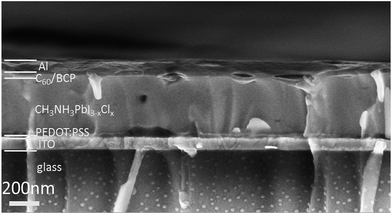 | ||
| Fig. 6 Cross-sectional image of the hybrid device produced in this study with a glass/ITO/PEDOT:PSS/orthorhombic CH3NH3PbI3 perovskite/C60/BCP/Al configuration. | ||
Conclusions
In conclusion, in this work we successfully demonstrated an electrospray technique to deposit solidified crystal precursors on the substrate and convert the solids to form an orthorhombic CH3NH3PbI3 active layer for fabricating perovskite-based hybrid solar cells. Depositing the solids by electrospraying improves the de-wetting of the layer when using the wet-coating process on the substrate. The applied voltages between the nozzle head and the ground electrode in the electrospray process modulate the uniformity and initial morphology of the deposited film. Thermal annealing at an elevated temperature improves the crystallinity and coverage of the perovskite film on the substrate. A hybrid cell made of the active layer produced by the electrospray process exhibits a VOC of 0.87 V, a JSC of 19.71 mA cm−2, and an FF of 0.55, corresponding to a PCE of 9.3%, which is comparable to the performance of a cell prepared by the conventional spin-coating process. The results indicate that the electrospray technique developed in this work would be ideal to achieve large-area coating of a perovskite active layer with the potential for real mass production. We understand that the morphology of the deposited film is still the key component to determining the photovoltaic parameters of the resulting cells. Intensive work to further advance the device performance is currently in progress.Acknowledgements
The authors would like to thank the National Science Council (NSC) (now Ministry of Science and Technology) in Taiwan (NSC102-2628-M-006-001-MY3), (MOST105-2119-M-024-001), the Asian Office of Aerospace Research and Development (AOARD-14-4012), and the CPC Corporation, Taiwan (MEA0300012) for financially supporting this research.References
- C. Wehrenfennig, G. E. Eperon, M. B. Johnston, H. J. Snaith and L. M. Herz, Adv. Mater., 2014, 26, 1584 CrossRef CAS PubMed.
- W. J. Yin, T. T. Shi and Y. F. Yan, Adv. Mater., 2014, 26, 4653 CrossRef CAS PubMed.
- G. C. Xing, N. Mathews, S. Y. Sun, S. S. Lim, Y. M. Lam, M. Grätzel, S. Mhaisalkar and T. C. Sum, Science, 2013, 342, 344 CrossRef CAS PubMed.
- S. D. Stranks, G. E. Eperon, G. Grancini, C. Menelaou, M. J. P. Alcocer, T. Leijtens, L. M. Herz, A. Petrozza and H. J. Snaith, Science, 2013, 342, 341 CrossRef CAS PubMed.
- J.-H. Im, C.-R. Lee, J.-W. Lee, S.-W. Park and N.-G. Park, Nanoscale, 2011, 3, 4088 RSC.
- A. Kojima, K. Teshima, Y. Shirai and T. Miyasaka, J. Am. Chem. Soc., 2009, 131, 6050 CrossRef CAS PubMed.
- M. M. Lee, J. Teuscher, T. Miyasaka, T. N. Murakami and H. J. Snaith, Science, 2012, 338, 643 CrossRef CAS PubMed.
- P. Docampo, J. M. Ball, M. Darwich, G. E. Eperon and H. J. Snaith, Nat. Commun., 2014, 4, 2761 Search PubMed.
- L. Etgar, P. Gao, Z. Xue, Q. Peng, A. K. Chandiran, B. Liu, M. K. Nazeeruddin and M. Grätzel, J. Am. Chem. Soc., 2012, 134, 17396 CrossRef CAS PubMed.
- J.-Y. Jeng, Y.-F. Chiang, M.-H. Lee, S.-R. Peng, T.-F. Guo, P. Chen and T.-C. Wen, Adv. Mater., 2013, 25, 3727 CrossRef CAS PubMed.
- H. Zhou, Q. Chen, G. Li, S. Luo, T.-b. Song, H.-S. Duan, Z. Hong, J. You, Y. Liu and Y. Yang, Science, 2014, 345, 542 CrossRef CAS PubMed.
- W. S. Yang, J. H. Noh, N. J. Jeon, Y. C. Kim, S. Ryu, J. Seo and S. I. Seok, Science, 2015, 348, 1234 CrossRef CAS PubMed.
- N. Ahn, D.-Y. Son, I.-H. Jang, S. M. Kang, M. Choi and N.-G. Park, J. Am. Chem. Soc., 2015, 137, 8696 CrossRef CAS PubMed.
- Q. Chen, H. Zhou, Z. Hong, S. Luo, H.-S. Duan, H.-H. Wang, Y. Liu, G. Li and Y. Yang, J. Am. Chem. Soc., 2014, 136, 622 CrossRef CAS PubMed.
- Z. Xiao, C. Bi, Y. Shao, Q. Dong, Q. Wang, Y. Yuan, C. Wang, Y. Gao and J. Huang, Energy Environ. Sci., 2014, 7, 2619 CAS.
- K. M. Boopathi, M. Ramesh, P. Perumal, Y.-C. Huang, C.-S. Tsao, Y.-F. Chen, C.-H. Lee and C.-W. Chu, J. Mater. Chem. A, 2015, 3, 9257 CAS.
- N. J. Jeon, J. H. Noh, Y. C. Kim, W. S. Yang, S. Ryu and S. I. Seok, Nat. Mater., 2014, 13, 897 CrossRef CAS PubMed.
- H. Ishihara, W. Chen, Y.-C. Chen, S. Sarang, N. D. Marco, O. Lin, S. Ghosh and V. C. Tung, Adv. Mater. Interfaces, 2016, 3, 1500762 CrossRef.
- P.-W. Liang, C.-Y. Liao, C.-C. Chueh, F. S. Zuo, T. Williams, X.-K. Xin, J. Lin and A. K.-Y. Jen, Adv. Mater., 2014, 26, 3748 CrossRef CAS PubMed.
- Y. Guo, K. Shoyama, W. Sato and E. Nakamura, Adv. Energy Mater., 2016, 6, 1502317 CrossRef.
- R. A. Wibowo, W. H. Jung, M. H. Al-Faruqi, I. Amal and K. H. Kim, Mater. Chem. Phys., 2010, 124, 1006 CrossRef CAS.
- W. K. Kim, S. Kim, E. A. Payzant, S. A. Speakman, S. Yoon, R. M. Kaczynski, R. D. Acher, T. J. Anderson, O. D. Crisalle, S. S. Li and V. Craciun, J. Phys. Chem. Solids, 2005, 66, 1915 CrossRef CAS.
- K. C. Hsu, Y. S. Fu, P. Y. Lin, I. T. Tang and J. D. Liao, Int. J. Photoenergy, 2013, 2013, 156964 Search PubMed.
- D. Son, S. M. Hughes, Y. D. Yin and A. P. Alivisatos, Science, 2004, 306, 1009 CrossRef CAS PubMed.
- B. Dudout, J. C. M. Marijnissen and B. Scarlett, J. Aerosol Sci., 1999, 30, 687 CrossRef.
- I. W. Lenggoro and K. Okuyama, J. Aerosol Sci., 1997, 28, 351 CrossRef.
- S. Basak, D. R. Chen and P. Biswas, Chem. Eng. Sci., 2007, 62, 1263 CrossRef CAS.
- K. Balasubramanian, S. N. Jayasinghe and M. J. Edirisinghe, Int. J. Appl. Ceram. Technol., 2006, 3, 55 CrossRef CAS.
- S. N. Jayasinghe, M. J. Edirisinghe and D. Z. Wang, Nanotechnology, 2004, 15, 1519 CrossRef CAS.
- Q. Z. Chen, A. R. Boccaccini, H. B. Zhang, D. Z. Wang and M. J. Edirisinghe, J. Am. Ceram. Soc., 2006, 89, 1534 CrossRef CAS.
- I. W. Lenggoro, K. Okuyama, J. F. de la Mora and N. Tohge, J. Aerosol Sci., 2000, 31, 121 CrossRef CAS.
- E. M. Kelder, O. C. J. Nijs and J. Schoonman, Solid State Ionics, 1994, 68, 5 CrossRef CAS.
- T. Nguyen and E. Djurado, Solid State Ionics, 2001, 138, 191 CrossRef CAS.
- B. Su, M. Wei and K. L. Choy, Mater. Lett., 2001, 47, 83 CrossRef CAS.
- R. Chandrasekhar and K. L. Choy, J. Cryst. Growth, 2001, 231, 215 CrossRef CAS.
- L. Rayleigh, Philosophical Magazine Series 5, 1882, 14, 184 CrossRef.
- L. Wannatong, A. Sirivat and P. Supaphol, Polym. Int., 2004, 53, 1851 CrossRef CAS.
- S. R. Raga, M.-C. Jung, M. V. Lee, M. R. Leyden, Y. Kato and Y. Qi, Chem. Mater., 2015, 27, 1597 CrossRef CAS.
- B. Wang, K. Y. Wong, X. Xiao and T. Chen, Sci. Rep., 2015, 5, 10557 CrossRef PubMed.
- I. Persson, K. Lyczko, D. Lundberg, L. Eriksson and A. Płaczek, Inorg. Chem., 2011, 50, 1058 CrossRef CAS PubMed.
- N. Yantara, F. Yanan, C. Shi, H. A. Dewi, P. P. Boix, S. G. Mhaisalkar and N. Mathews, Chem. Mater., 2015, 27, 2309 CrossRef CAS.
- T.-B. Song, Q. Chen, H. Zhou, C. Jiang, H.-H. Wang, Y. M. Yang, Y. Liu, J. You and Y. Yang, J. Mater. Chem. A, 2015, 3, 9032 CAS.
| This journal is © The Royal Society of Chemistry 2017 |

