
 Open Access Article
 This Open Access Article is licensed under a Creative Commons Attribution-Non Commercial 3.0 Unported Licence
UV-enhanced atomic layer deposition of Al2O3 thin films at low temperature for gas-diffusion barriers†
Kwan Hyuck Yoon‡
,
Hongbum Kim‡,
Yong-Eun Koo Lee,
Nabeen K. Shrestha and
Myung Mo Sung*
and
Myung Mo Sung*
Department of Chemistry, Hanyang University, Seoul, 04763, Republic of Korea. E-mail: smm@hanyang.ac.kr
First published on 18th January 2017
Abstract
We present ultraviolet (UV) enhanced atomic layer deposition (ALD), UV-ALD, as a promising approach to deposit effective gas-diffusion barrier thin films. Highly dense, uniform, and conformal Al2O3 thin films were prepared by UV-ALD at 40 °C, suggesting that UV irradiation during the ALD process promotes the reactions to achieve an ideal ALD process even at low temperature. The water-diffusion barrier performance of the Al2O3 thin films was found to be significantly enhanced by the use of UV irradiation. The water vapor transmission rate of Al2O3 films grown by UV-ALD at 40 °C was estimated to be 9.20 × 10⁻⁷ g m−2 d−1 using a Ca conductance test, which is one of the lowest reported WVTR values among the ALD Al2O3 barrier thin films and satisfies the WVTR requirement of 10−6 g m−2 d−1. The WVTR measurements were also performed by MOCON testing using 10–100 nm thick Al2O3 thin films on PET substrates, also showing superior performance of the UV-ALD thin films to that of the thermal ALD film. All the UV-ALD films except the 10 nm-thick one show WVTR values below 1.00 × 10⁻³ g m−2 d−1, the detection limit of the MOCON instrument used.
1. Introduction
Organic light emitting diodes (OLEDs) have been known as a promising display technology with their advantages in terms of natural color reproduction, low voltage operation, ultra-thin structure, and mechanical flexibility.1–3 It is well known that a primary obstacle to commercialization of OLEDs is their extremely high sensitivity to moisture and oxygen.4,5 Moreover, plastic substrates used for flexible OLED devices offer little protection against water and oxygen, resulting in rapid degradation of the devices.6–8 Consequently, development of effective gas-diffusion barriers has been a key issue for OLED devices. For an adequate lifespan of the OLEDs, the water-vapor transmission rate (WVTR) of the gas-diffusion barrier is required to be 10−6 g m−2 d−1 or less.8,9 Atomic layer deposition (ALD) has emerged as a promising method to prepare the barriers that meet such WVTR requirements because it allows the deposition of ultra-thin, uniform, and conformal films.10–13 Several studies reported the use of ALD to prepare gas-diffusion barrier films made of various inorganic materials.14–23 In particular, Al2O3 has been considered as an attractive choice for barrier materials against moisture and oxygen.19–23 Unfortunately, the ALD process has not yet been successful to prepare effective Al2O3 barrier thin films for OLEDs. This is probably because the substrate temperature during the ALD process should be kept low, below 80 °C, so as to avoid thermal damage on the temperature-sensitive organic materials in OLEDs24,25 and plastic substrates.26,27 The temperature (<80 °C) is too low to provide enough thermal energy for all the surface reactions to complete.12,18,23,28 The ALD Al2O3 films were low-density films with a large amount of hydroxyl groups and carbon-related impurities when prepared at low temperature (<200 °C).28–31Some recent studies attempted to overcome the problems by adopting the plasma-enhanced ALD (PE-ALD) which can produce high-quality thin film for gas-diffusion barrier at low temperature.32–36 However, none of these Al2O3 thin films grown by PE-ALD have met the WVTR requirement to be used for OLEDs.37 Moreover, PE-ALD technique has a critical drawback: the organic materials in OLEDs are exposed to a flux of highly energetic atoms or charge particles from plasma.22,38,39 Therefore, it seems crucial to develop efficient low-temperature thin film encapsulation (TFE) process.
ALD assisted by UV irradiation has also been used for enhanced growth of metal oxide thin films.40–47 In our previous report, uniform and conformal ZrO2 thin films were deposited on plastic substrates at room temperature (RT) by UV-enhanced ALD (UV-ALD).43 One can expect that high-quality Al2O3 thin films may be obtained at low deposition temperature by using UV-ALD. However, only a couple of cases have been reported for the use of the UV-ALD to prepare Al2O3 thin film and their deposition temperatures were not limited to low temperature.42,44 Moreover, these works are focused on the effect of UV irradiation on growth mechanism or electrical properties of the films, not on their barrier performance for OLEDs applications.
Herein, we developed high quality Al2O3 thin films as efficient gas-diffusion barrier films for OLEDs by adopting the UV-ALD at low temperature. Strikingly, the density of Al2O3 film was improved from 2.59 g cm−3 to 3.01 g cm−3 by employing UV light irradiation during the ALD process at 40 °C. The Al2O3 thin film grown by the UV-ALD exhibited the WVTR of 9.20 × 10⁻⁷ g m−2 d−1, manifesting its excellent barrier performance. These results demonstrate that the UV-ALD process can be a promising approach to fabricate Al2O3 film for TFE application on plastic substrates.
2. Experimental methods
2.1. Preparation of substrates
Various substrates (e.g., Si, glass, and plastic) were used in the study. The Si substrates employed in this study were cut from p-type (100) Si wafers (LG Siltron) with resistivity in the range of 1 to 5 Ω cm. The Si substrates were initially treated with a chemical cleaning process that involved degreasing, HNO3 boiling, NH4OH boiling (alkali treatment), HCl boiling (acid treatment), rinsing in deionized water, and blow-drying with nitrogen to remove contaminants and to grow a thin protective oxide layer on the surface.48 The glass substrates were cleaned with acetone, ethanol, de-ionized water, and blow-dried with nitrogen to remove contaminants. The plastic substrates were cut from polyethylene terephthalate (PET) films (Melinex ST504, 125 μm). Before using, the substrates were cleaned in de-ionized water and ethanol, and blow-dried with nitrogen to remove contaminants.2.2. Deposition of Al2O3 film via UV-ALD
Al2O3 thin films were deposited onto the substrates using trimethylaluminum (TMA, 97% Sigma-Aldrich) and water as aluminum and oxygen precursors, respectively. Argon (Ar) served as a carrier and purging gas at a rate of 100 sccm. The TMA and water were evaporated at 20 °C. For enhancing the ALD reaction, 400 W Hg lamp was installed between hot and cold mirrors to have a working distance of 10 cm from the substrate, as shown in Fig. 1a. The hot mirror was used to reflect IR and visible lights, while the cold mirror was used as an UV radiation reflector. When IR and visible lights from the Hg lamp were filtered out, only broad spectrum of UV-C (200–280 nm) light was focused on the substrate and the substrate temperature was kept constant, as illustrated in Fig. S1.† The total intensity of the UV light at the substrate surface was 4 W cm−2. The detailed sequence of UV-ALD cycle is shown in Fig. 1b. Briefly, each ALD cycle consists of 1 s exposure of the substrate to TMA vapor, 15 s of Ar-purge to remove physisorbed TMA, 2 s exposure to water vapor with UV irradiation, additional UV irradiation for 0–4 s, and then 30 s of Ar-purge. The substrate temperature was maintained at 40 °C by a substrate holder with a water cooling system. | ||
| Fig. 1 (a) Schematic diagram of an ALD system equipped with a UV lamp. Cold mirror and hot mirror reflect UV radiation and visible/IR radiation, respectively. Note that the hot mirror prevents the substrate temperature from increasing. (b) UV-ALD sequence used for current study. (c) Sequential surface reactions to fabricate Al2O3 thin films on a substrate using UV-ALD. | ||
2.3. Film characterization
The film thickness and refractive index of Al2O3 films were measured using spectroscopic ellipsometer (Elli-SE, Ellipso Technology). Film density was characterized using X-ray reflectivity (XRR, PANalytical X'Pert PRO) with a Cu Kα X-ray tube (1.54 Å) operated at 40 kV and 30 mA. The experimentally obtained XRR spectra were fitted using X'Pert Reflectivity program. Chemical composition of the film was determined using X-ray photoelectron spectroscopy (XPS, PHI 5000 VersaProbe, Ulvac-PHI) with an Al Kα X-ray line (1486.6 eV) operated at 15 kV. The binding energy of each element was calibrated using C 1s peak (284.6 eV). Film morphology was investigated by atomic force microscopy (AFM, XE-100). Contact angle between a water-droplet and the film surface was measured by the contact angle meter (A-100 Ramι-Hart goniometer).For quantitative evaluation of barrier performance of the Al2O3 films deposited on glass substrates, their WVTRs were measured indirectly using calcium (Ca) conductance test under two different acceleration conditions, 85 °C, 85% RH and 70 °C, 90% RH. The conductance measurements for the Ca test were taken using a semiconductor parameter analyzer (HP 4155C, Agilent Technologies). Furthermore, visual evaluation of the barrier films under the acceleration condition at 85 °C and 85% RH was also performed using an array of Ca dots. In case of the Al2O3 films on PET substrates (10 cm × 10 cm), the WVTRs were directly measured by MOCON test (Permatran-W 3/33 MA) at 37.8 °C and 100% RH.
3. Results and discussion
3.1. ALD growth of Al2O3 thin film and influence of UV irradiation
Fig. 1c shows a schematic diagram for Al2O3 film growth by UV-ALD. When TMA is injected into the reactor, it is chemisorbed on the substrate-surface via ligand exchange reactions with hydroxyl groups that are rich in the surface.12 As a result, volatile CH4 by-products are released and –O–Al(CH3)2 species are attached to the surface by covalent bonding.12 In the subsequent ALD half-reaction, H2O vapor reacts with the –O–Al(CH3)2 to form –O–Al(OH)2 and CH4 by-products.12 During this second half of the ALD process, UV light is irradiated on the surface, which assists the reaction between H2O and –O–Al(CH3)2 surface group to form Al2O3 by removing –CH3 groups via photo-dissociation.49–52The surface reactions during the ALD process must be self-terminating and complementary to yield a uniform and conformal Al2O3 thin film. To verify the self-terminating nature of Al2O3, dosing times for TMA and water were varied between 0.5 and 5 s and a constant Ar purging time of 120 s were used. The UV irradiation was applied during the water dosing stage. The UV irradiation time was equal to the water dosing period for the period from 0.5 to 2 s, but it was fixed to be 2 s for the period longer than 2 s. A constant temperature of 40 °C was maintained for the substrate during the entire ALD process. For comparison, deposition of Al2O3 thin films was also performed by thermal ALD process, i.e., ALD without UV irradiation, under the same experimental conditions. The growth per cycle (GPC) of each Al2O3 films was measured by an ellipsometry (Fig. S2a and b†). The GPC values by both UV-ALD and thermal ALD became saturated when the dosing pulses of TMA and H2O exceeded 1 s and 2 s, respectively. On the other hand, a longer Ar purging time after H2O dosing step was required for the thermal ALD than for the UV-ALD, 120 s vs. 30 s, to reach the saturation level of the GPC values, as shown in Fig. S2c.† This indicates that there were excessive H2O molecules condensed on the surface during the ALD process probably due to low surface temperature,28 and that the UV irradiation eliminated the redundant water molecules effectively. The film growth was linear as a function of the number of ALD cycles for both cases but the growth rate was higher under UV irradiation (Fig. S2d†). Thus, these results demonstrate that the self-terminating surface reaction for ALD of the Al2O3 thin films at 40 °C can be enhanced by applying UV irradiation.
The effect of UV irradiation during ALD process on the Al2O3 film properties was investigated by extending the irradiation for additional time periods, 0–4 s, beyond the 2 s of H2O dosing stage (Fig. 2a–c). The substrate temperature was maintained at 40 °C during the UV-ALD process. For comparison, the Al2O3 films were also prepared by thermal ALD at various temperatures ranging from 40 to 200 °C, as shown in Fig. 2d–f. For each Al2O3 film prepared under different conditions, the GPC, density, and refractive index of the film were measured.
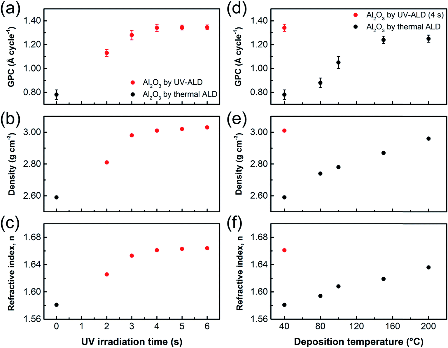 | ||
| Fig. 2 Effect of UV irradiation time and temperature on Al2O3 thin films grown by ALD. (a) Growth per cycle (GPC), (b) density, and (c) refractive index of the film grown at 40 °C as a function of UV irradiation time (2 s in H2O dosing step and 0–4 s for additional exposure in purging step); (d) GPC, (e) density, and (f) refractive index of the film as a function of temperature. The UV-ALD data shown in (d–f) are obtained using a UV irradiation time of 4 s. | ||
Fig. 2a shows the GPC of the Al2O3 films as a function of UV irradiation time. The GPC increased with UV irradiation time and attained the saturation levels when the total irradiation time reached 4 s (i.e., 2 s during H2O dosing step, plus 2 s additional irradiation time during Ar-purge). The saturated GPC value was 1.34 Å per cycle. In contrast, the GPC of the Al2O3 film by thermal ALD was 0.78 Å per cycle at 40 °C, which increased gradually with temperature and reached the stationary level of 1.25 Å per cycle at 150 °C (Fig. 2d). The lower GPCs at temperatures below 150 °C is probably due to insufficient thermal energy for completing the ALD reactions over entire substrate surface. This finding suggests that UV irradiation can serve as an additional energy source to help achieve an ideal ALD process even at low temperature.
Fig. 2b and e show the effect of UV irradiation time and temperature on the densities of the Al2O3 films, respectively. The densities were estimated by XRR measurements and simulation to find well-fitted curves. XRR spectra of the 50 nm-thick Al2O3 thin films grown by ALD at 40 °C with and without UV irradiation and their well-fitted simulated curves are shown in Fig. S3a.† The two different samples show similar spacing between the periodic fringes, suggesting that both samples have a similar film thickness. Film densities were obtained from the critical angles of the XRR spectra, as shown in inset of Fig. S3a.† When the ALD reaction was performed at 40 °C under UV irradiation for 4 s and up, the film density reached a constant level of 3.01 g cm−3 (Fig. 2b). In contrast, the film density by thermal ALD was only 2.59 g cm−3 at 40 °C, which was brought to the same level as that by the UV-ALD when the deposition temperature increased to 200 °C (Fig. 2e). This implies that pinholes may exist in the Al2O3 film grown by thermal ALD at temperature lower than 200 °C. It seems that UV irradiation during ALD process effectively prevents the generation of pinholes in the film prepared at temperature as low as 40 °C.
The refractive indices of the Al2O3 thin films were measured using spectroscopic ellipsometry. Typical ellipsometry spectra of the Al2O3 thin films grown at 40 °C by thermal and UV-ALD are shown in Fig. S3b.† The refractive indices at 633 nm were measured for the Al2O3 thin films grown by UV-ALD and thermal ALD reactions, as shown in Fig. 2c and f. Similar to the GPC and film density, the refractive indices of the films increased and then leveled off as the UV irradiation time and deposition temperature increased. The refractive index of the Al2O3 thin films grown at 40 °C under UV irradiation for 4 s was 1.66 while it was only 1.58 at 40 °C and increased up to 1.64 at 200 °C when UV irradiation was not applied. These low refractive indices of the films by thermal ALD may be due to the low film densities and/or the presence of impurities such as hydroxyl- and carbon-containing ones.53–56 Under UV irradiation for a sufficiently long period of time (i.e., at least 4 s in the present case), the generation of impurities may be avoided by photo-induced removal of the –OH groups and loosely bonded H2O molecules as well as by photo-dissociation of surface-adsorbed TMA leading to removal of –CH3 groups from the film surface.42
3.2. Influence of UV irradiation on chemical composition of Al2O3 thin film
To gain insight into the influence of UV irradiation on chemical composition of the Al2O3 thin film, XPS study on the films grown at 40 °C by thermal ALD and UV-ALD was performed. Fig. 3a shows high resolution XPS spectra for Al 2p core level of the two Al2O3 thin films, one with a peak centering at 74.95 eV (thermal ALD film) and the other one with a peak at 74.60 eV (UV-ALD film). The different peak positions for the two Al2O3 thin films suggest that there may be additional types of bonds other than O–Al–O bond. The Al 2p XPS spectra were deconvoluted to show two components corresponding to O–Al–O (i.e., bond in Al2O3) peak centering at the binding energy of 74.55 eV (red spectra), and –OH/AlOOH (i.e., bond in AlOOH or Al(OH)3) peak centering at the binding energy of 75.25 eV (blue spectra).57 Similarly, high resolution XPS spectra for O 1s core level show that there is a notable difference in the binding energy, about 1 eV, between the two Al2O3 films (Fig. 3b). The O 1s spectra were also deconvoluted into two components consisting of O–Al–O oxide peak (red spectrum) centering at 531.00 eV, and –OH/AlOOH hydroxide peak (blue spectrum) centering at about 532.30 eV.57 The deconvoluted spectra reveal interesting facts. In case of the Al2O3 films by UV-ALD, the Al 2p and the O 1s spectra reveal that the relative intensity and the area under the peaks corresponding to O–Al–O bonds are much larger than those of the –OH/AlOOH bonds (Fig. 3a and b, top). However, an opposite situation in the relative intensity and the area under the peaks is observed in the case of the films by thermal ALD (Fig. 3a and b, bottom). These XPS study results show that the thermal ALD Al2O3 film contains a lot of unreacted –OH groups, while the UV-ALD film is composed mainly of O–Al–O species, despite the same low deposition temperature. This suggests that the UV irradiation during the ALD process helped complete the ALD reactions that were otherwise inefficient and incomplete due to low thermal energy at 40 °C. Consequently, the UV-ALD films would have higher GPC, density, and refractive index than the thermal ALD films at the same temperature, as already demonstrated in Fig. 2 above.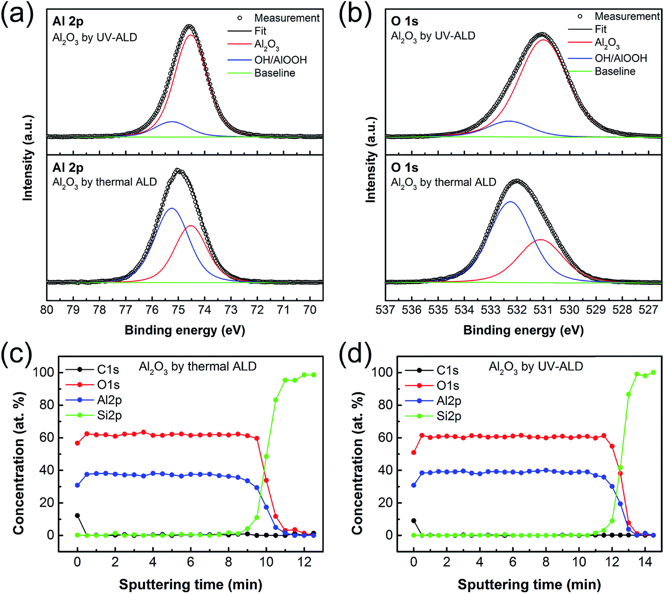 | ||
| Fig. 3 High resolution XPS spectra for the (a) Al 2p, (b) O 1s core level of Al2O3 thin films by thermal ALD and UV-ALD at 40 °C. XPS depth profiles for the Al2O3 thin film grown at 40 °C by (c) thermal ALD and (d) UV-ALD. | ||
Depth profiles of the two films were also studied using XPS so as to find the various elements present and their spatial distribution throughout the films. The depth profiles reveal there are no depth-dependent variations in the amount of Al and O throughout the films as shown in Fig. 3c and d. However, the amount ratio of O to Al in the two samples are different. For the film obtained by UV-ALD at 40 °C, the O/Al ratio is found to be 1.56, which is closer to the theoretical stoichiometric value of 1.5 for Al2O3. In contrast, the film by thermal ALD shows the O/Al ratio of 1.66. The excessive O for the film by thermal ALD may be related to the large concentration of –OH species incorporated into the film, as discussed above. The carbon contents in the thermal ALD and UV-ALD films were also estimated from the depth profiles in Fig. 3c and d. It was found that the thermal ALD process yielded comparatively higher carbon content (0.36 atomic %) in the films than did the UV-ALD process (0.07 atomic %). We suppose that carbon atoms in the films originate from the surface-adsorbed –O–Al(CH3)2 during the ALD process. The difference in the carbon content also suggests what we found above: thermal energy at 40 °C is not sufficient enough to complete the ALD reactions and the UV irradiation facilitate the removal of –CH3 groups.
3.3. ALD growth of Al2O3 thin film on PET substrate under UV irradiation
Generally, plastic substrates employed in flexible electronics require a suitable low temperature processing technique for deposition of uniform and ultra-thin film of Al2O3. In the present study, Al2O3 thin film on PET substrate was deposited by ALD at 40 °C with and without UV irradiation. Fig. S4† shows the macroscopic surface properties of the Al2O3 thin film studied by performing contact angle analysis. The PET substrates were employed in the deposition processes, just after being cleaned with de-ionized water and ethanol, and dried, without further treatment for activating the surfaces. When the ALD process was performed without UV irradiation, the contact angle of water decreased gradually with ALD cycles. In general, the Al2O3 surface shows intrinsically hydrophilic behavior.58 The slow gradual decrease in the contact angles on the thermal ALD films with ALD cycles suggest that the films grew by island-like growth mechanism.59,60 In contrast, when the ALD reactions were assisted by UV irradiation, the contact angle of water on the Al2O3 deposited PET surface drops to a stationary level after only five ALD cycles, indicating layer-by-layer film growth. Further, microscopic surface analysis of the Al2O3 film on PET substrate, deposited by 100 cycles of ALD with a thickness of approximately 10 nm, was performed using AFM. As evident from AFM images shown in Fig. S5,† the film obtained by thermal ALD is rather coarse with abundant texture, showing a root-mean-square (RMS) surface roughness of 6.38 nm that is a lot higher than that of bare PET (3.13 nm) (Fig. S5a and b†). However, a uniform and smooth surface with a RMS surface roughness of 3.34 nm, very close to that of bare PET, was observed in the case of the film grown by UV-ALD (Fig. S5c†). These roughness results also suggest different mechanisms for film growth in the two cases. It seems that UV irradiation activates the PET surface effectively for the chemisorption of ALD precursors on the surface as well as promotes the surface reactions. Thus, the surface-terminating layer-by-layer deposition of Al2O3 was achieved uniformly over entire PET surface by UV-ALD at 40 °C. These results also demonstrate that the PET surface was not degraded by UV-ALD process under the experimental condition used. We note that the surface roughness is expected to increase because of debris or sinkage if the surface is damaged.3.4. Water diffusion barrier properties of Al2O3 thin films
Water diffusion barrier characteristics of the Al2O3 thin films grown at low temperature by thermal ALD and UV-ALD were evaluated quantitatively by measuring water vapor permeability of the films both directly and indirectly. Firstly, the water-vapor transmission rate (WVTR) for each type of the films was measured indirectly using the Ca conductance test method,61 which involves the monitoring of Ca degradation by measuring the conductance change with time exposed to various degree of water content environments. Briefly, the testing procedure was as follows. First, a device consisting of 200 nm-thick thermally evaporated Ca electrode between two Ag electrodes separated by a distance of 500 μm on a glass substrate was constructed and then encapsulated with a 100 nm-thick Al2O3 thin film, as shown in the inset of Fig. 4a. Second, the devices were then stored under following two acceleration conditions: (i) 85 °C and 85% relative humidity (RH); (ii) 70 °C and 90% RH. Fig. 4a and b show the changes in the conductance of the Ca electrode as a function of the exposure time to the two acceleration conditions. Based on the standard equation of permeation given elsewhere,61 and the conductance data with respect to the exposure time, WVTRs of the 100 nm-thick Al2O3 thin films by thermal ALD and UV-ALD were obtained as summarized in Table 1. The permeation rates represent the mean values from 10 test samples. There is a significant improvement in the WVTR values by the use of UV irradiation during ALD process. Notably, the estimated WVTR value at room temperature for the UV-ALD Al2O3 film was 9.20 × 10⁻⁷ g m−2 d−1, which is one of the lowest WVTR values among the ALD Al2O3 barrier thin films ever reported. For more comparison, previous reports on selected Al2O3 thin films that were deposited at low ALD reaction temperatures and demonstrated an excellent barrier property against moisture are summarized in Table S1.† It should be noted that this quantitative barrier performance satisfies the WVTR requirement of 10−6 g m−2 d−1 that is the desired goal of the OLEDs industry. | ||
| Fig. 4 Barrier performance of the Al2O3 thin films deposited at 40 °C by thermal ALD and UV-ALD. Ca conductance test results under two different acceleration conditions (a) 70 °C, 90% RH and (b) 85 °C, 85% RH. The inset in (a) shows the device structure on a glass substrate. (c) Visual test results under an accelerated condition of 85 °C, 85% RH, using Ca dot arrays on glass substrates that are encapsulated by the Al2O3 thin films. The visible optical changes indicate the corrosion of Ca (black) into calcium oxide (transparent) by permeated water vapor. (d) Variation of WVTR of the films on PET substrate by MOCON test as a function of film thickness, (e) MOCON test results to obtain the WVTR for the 100 nm-thick Al2O3 barrier films by thermal ALD and UV-ALD. With time, WVTR values reach a constant level that is assigned as the final WVTR value by MOCON test. The detection limit of the MOCON instrument used was 1.00 × 10⁻³ g m−2 d−1. | ||
| Deposition type of Al2O2 film | WVTR in conditiona [g m−2 d−1] | WVTR in conditionb [g m−2 d−1] | Calculated WVTR at RT [g m−2 d−1] |
|---|---|---|---|
| a Acceleration condition of 70 °C, 90% RH.b 85 °C, 85% RH. | |||
| Thermal ALD | 2.61 (±0.16) × 10−3 | 9.23 (±0.25) × 10−3 | 8.14 (±2.09) × 10−6 |
| UV-ALD | 4.61 (±0.52) × 10−4 | 1.84 (±0.19) × 10−3 | 9.20 (±1.08) × 10−7 |
Secondly, a visual barrier test was also performed using Ca probe consisting of a thermally deposited array of 144 square-shaped Ca dots (0.50 mm × 0.50 mm) on a glass substrate. The array of Ca dots was subsequently encapsulated with a 100 nm-thick Al2O3 barrier film, either by thermal ALD or UV-ALD, and was exposed to a controlled accelerated environment of 85 °C and 85% RH. This method is based on the visual monitoring of the optical changes accompanying the corrosion of the Ca dots, because Ca metal (black dot) converts to calcium oxide (transparent dot) as water vapor permeates through the barrier film.62 Fig. 4c shows the photographs of the Ca dot arrays encapsulated by barrier films after exposing to the accelerated environment for various periods of time. The Ca dot array encapsulated with the thermal ALD based Al2O3 barrier film (Top row) showed the complete oxidation of 31, 57, 89, and 144 Ca dots in 24, 120, 360, and 720 h, respectively. Thus, about 22% of the total Ca dots were completely oxidized just in 24 h exposure, and the entire Ca dots were oxidized in 720 h exposure. The rapid oxidation of Ca dots is attributed to the pinholes in the Al2O3 thin film deposited by thermal ALD at low temperature, which form direct pathways for water-vapor permeation throughout the film.63,64 However, a significantly better barrier performance was observed by the UV-ALD based Al2O3 barrier film (Bottom row): only 5, 14, and 21 Ca dots were oxidized in 120, 360, and 720 h, respectively. Less than 4% of the total Ca dots were found to be oxidized in 120 h exposure, while only 15% of the total Ca dots were oxidized in 720 h.
Thirdly, direct measurement of WVTRs was performed for Al2O3 thin films deposited on PET substrates, by MOCON test under the standard exposure environment (i.e., 37.8 °C, 100% RH). Two types of Al2O3 barrier films on a PET substrate, each with the film thickness ranging from 10 nm to 100 nm, were prepared by thermal ALD and UV-ALD respectively, and subject to MOCON test. Fig. 4d shows the variation of measured WVTR values by MOCON test with respect to film thickness and Fig. 4e shows representative MOCON test results to obtain the WVTR values. In general, thicker the film is, harder the water vapor passes through.65 In case of the thermal ALD Al2O3 films, such trend was observed (Fig. 4d). However, their barrier performances are all very poor. For example, the 10 nm-thick Al2O3 film exhibited a WVTR value of 6.11 × 10⁻¹ g m−2 d−1 which is close to that of bare PET substrate.7,8 The 100 nm-thick film showed a WVTR value of 5.79 × 10⁻³ g m−2 d−1 which is considered to be still much higher than the WVTR value required for OLEDs' barrier film. In case of the UV-ALD Al2O3 films, the 10 nm thick film showed an average WVTR value of 1.42 × 10⁻³ g m−2 d−1 that is even lower than that of the 100 nm-thick thermal ALD barrier film. Moreover, the MOCON WVTR results for the other thicker Al2O3 films by UV-ALD are all below the detection limit of the MOCON test instrument used, 1.00 × 10⁻³ g m−2 d−1. These results implies that the Al2O3 film obtained by UV-ALD is capable of effective TFE of plastic substrates despite the low deposition temperature (40 °C) and the ultra-low film thickness (≤100 nm).
4. Conclusions
UV irradiation was employed during ALD process, enabling the deposition of dense and conformal thin film of Al2O3 at low-temperature of 40 °C. Growth rate, density and refractive index of the films obtained under UV irradiation were found to be substantially higher than those of the films obtained without UV irradiation. Most importantly, the barrier performance of the films was significantly enhanced by the use of UV irradiation during ALD, reaching the desired level for OLEDs applications. The estimated WVTR value at room temperature for the 100 nm-thick UV-ALD Al2O3 film was 9.20 × 10⁻⁷ g m−2 d−1, which is one of the lowest WVTR values among the ALD Al2O3 barrier thin films ever reported. The enhanced barrier performance is attributed to the fact that the UV irradiation reconstructs the surface functional groups by removing loosely bonded unreacted reaction residues from the reaction surface. In addition, the UV irradiation assists self-terminating surface reactions to produce defect-less, dense, uniform, and conformal thin film of Al2O3. Importantly, this study demonstrates that UV-ALD can deposit high-quality conformal films on thermally unstable substrates.Acknowledgements
This work was supported by the Nano-Material Technology Development Program (2012M3A7B4034985) and by the Creative Materials Discovery Program (2015M3D1A1068061) through the National Research Foundation of Korea (NRF) funded by the Ministry of Science, ICT & Future Planning. This work was also supported by a grant from the National Research Foundation of Korea (NRF), funded by the Korea government (MSIP) (No. 2014R1A2A1A10050257).References
- C. W. Tang and S. A. VanSlyke, Appl. Phys. Lett., 1987, 51, 913 CrossRef CAS.
- G. Gu, P. Burrows, S. Venkatesh, S. R. Forrest and M. E. Thompson, Opt. Lett., 1997, 22, 172 CrossRef CAS PubMed.
- S. Chen, L. Deng, J. Xie, L. Peng, L. Xie, Q. Fan and W. Huang, Adv. Mater., 2010, 22, 5227 CrossRef CAS PubMed.
- P. E. Burrows, V. Bulovic, S. R. Forrest, L. S. Sapochak, D. M. McCarty and M. E. Thompson, Appl. Phys. Lett., 1994, 65, 2922 CrossRef CAS.
- Y. F. Liew, H. Aziz, N. X. Hu, H. S. O. Chan, G. Xu and Z. Popovic, Appl. Phys. Lett., 2000, 77, 2650 CrossRef CAS.
- M. S. Weaver, L. A. Michalski, K. Rajan, M. A. Rothman, J. A. Silvernail, J. J. Brown, P. E. Burrows, G. L. Graff, M. E. Gross, P. M. Martin, M. Hall, E. Mast, C. Bonham, W. Bennett and M. Zumhoff, Appl. Phys. Lett., 2002, 81, 2929 CrossRef CAS.
- Y. Leterrier, Prog. Mater. Sci., 2003, 48, 1 CrossRef CAS.
- J. S. Lewis and M. S. Weaver, IEEE J. Sel. Top. Quantum Electron., 2004, 10, 45 CrossRef CAS.
- P. E. Burrows, G. L. Graff, M. E. Gross, P. M. Martin, M. Hall, E. Mast, C. C. Bonham, W. D. Bennett, L. A. Michalski, M. S. Weaver, J. J. Brown, D. Fogarty and L. S. Sapochak, presented at Proc. SPIE4105, 2001 Search PubMed.
- T. Suntola, Mater. Sci. Rep., 1989, 4, 261 CrossRef CAS.
- M. Leskela and M. Ritala, Thin Solid Films, 2002, 409, 138 CrossRef CAS.
- S. M. George, Chem. Rev., 2010, 110, 111 CrossRef CAS PubMed.
- H. Shin, D. K. Jeong, J. Lee, M. M. Sung and J. Kim, Adv. Mater., 2004, 16, 1197 CrossRef CAS.
- W. S. Kim, M. G. Ko, T. S. Kim, S. K. Park, Y. K. Moon, S. H. Lee, J. G. Park and J. W. Park, J. Nanosci. Nanotechnol., 2008, 8, 4726 CrossRef CAS PubMed.
- J. Meyer, H. Schmidt, W. Kowalsky, T. Riedl and A. Kahn, Appl. Phys. Lett., 2010, 96, 243308 CrossRef.
- S. W. Seo, E. Jung, H. Chae and S. M. Cho, Org. Electron., 2012, 13, 2436 CrossRef CAS.
- C. Y. Chang, C. T. Chou, Y. J. Lee, M. J. Chen and F. Y. Tsai, Org. Electron., 2009, 10, 1300 CrossRef CAS.
- M. H. Tseng, H. H. Yu, K. Y. Chou, J. H. Jou, K. L. Lin, C. C. Wang and F. Y. Tsai, Nanotechnology, 2016, 27, 295706 CrossRef PubMed.
- M. D. Groner, S. M. George, R. S. McLean and P. F. Carcia, Appl. Phys. Lett., 2006, 88, 051907 CrossRef.
- P. F. Carcia, R. S. McLean, M. H. Reilly, M. D. Groner and S. M. George, Appl. Phys. Lett., 2006, 89, 031915 CrossRef.
- J. A. Bertrand and S. M. George, J. Vac. Sci. Technol., A, 2013, 31, 01A122 Search PubMed.
- Y. Q. Yang, Y. Duan, P. Chen, F. B. Sun, Y. H. Duan, X. Wang and D. Yang, J. Phys. Chem. C, 2013, 117, 20308 CAS.
- Y. Q. Yang, Y. Duan, Y. H. Duan, X. Wang, P. Chen, D. Yang, F. B. Sun and K. W. Xue, Org. Electron., 2014, 15, 1120 CrossRef CAS.
- X. Zhou, J. He, L. S. Liao, M. Lu, X. M. Ding, X. Y. Hou, X. M. Zhang, X. Q. He and S. T. Lee, Adv. Mater., 2000, 12, 265 CrossRef CAS.
- H. C. Yeh, H. F. Meng, H. W. Lin, T. C. Chao, M. R. Tseng and H. W. Zan, Org. Electron., 2012, 13, 914 CrossRef CAS.
- J. F. Silvain, A. Veyrat and J. J. Ehrhardt, Thin Solid Films, 1992, 221, 114 CrossRef CAS.
- P. F. Carcia, R. S. McLean, M. D. Groner, A. A. Dameron and S. M. George, J. Appl. Phys., 2009, 106, 023533 CrossRef.
- M. D. Groner, F. H. Fabreguette, J. W. Elam and S. M. George, Chem. Mater., 2004, 16, 639 CrossRef CAS.
- M. D. Groner, J. W. Elam, F. H. Fabreguette and S. M. George, Thin Solid Films, 2002, 413, 186 CrossRef CAS.
- E. Langereis, M. Bouman, J. Keijmel, S. B. S. Heil, M. C. M. van de Sanden and W. M. M. Kessels, ECS Trans., 2008, 16, 247 CrossRef CAS.
- S. E. Potts, W. Keuning, E. Langereis, G. Dingemans, M. C. M. van de Sanden and W. M. M. Kessels, J. Electrochem. Soc., 2010, 157, P66 CrossRef CAS.
- E. Langereis, M. Creatore, S. B. S. Heil, M. C. M. van de Sanden and W. M. M. Kessels, Appl. Phys. Lett., 2006, 89, 081915 CrossRef.
- S. J. Yun, Y. W. Ko and J. W. Lim, Appl. Phys. Lett., 2004, 85, 4896 CrossRef CAS.
- H. G. Kim and S. S. Kim, Thin Solid Films, 2011, 520, 481 CrossRef CAS.
- J. G. Lee, H. G. Kim and S. S. Kim, Thin Solid Films, 2013, 534, 515 CrossRef CAS.
- H. Jung, H. Choi, H. Jeon, S. Lee and H. Jeon, J. Appl. Phys., 2013, 114, 173511 CrossRef.
- J. S. Park, H. Chae, H. K. Chung and S. I. Lee, Semicond. Sci. Technol., 2011, 26, 034001 CrossRef.
- L. S. Liao, L. S. Hung, W. C. Chan, X. M. Ding, T. K. Sham, I. Bello, C. S. Lee and S. T. Lee, Appl. Phys. Lett., 1999, 75, 1619 CrossRef CAS.
- S. Han, X. Feng, Z. H. Lu, D. Johnson and R. Wood, Appl. Phys. Lett., 2003, 82, 2715 CrossRef CAS.
- K. Saito, Y. Watanabe, K. Takahashi, T. Matsuzawa, B. Sang and M. Konagai, Sol. Energy Mater. Sol. Cells, 1997, 49, 187 CrossRef CAS.
- J. C. Kwak, Y. H. Lee and B. H. Choi, Appl. Surf. Sci., 2004, 230, 249 CrossRef CAS.
- S. Y. No, D. Eom, C. S. Hwang and H. J. Kim, J. Electrochem. Soc., 2006, 153, F87 CrossRef CAS.
- B. H. Lee, S. Cho, J. K. Hwang, S. H. Kim and M. M. Sung, Thin Solid Films, 2010, 518, 6432 CrossRef CAS.
- P. R. Chalker, P. A. Marshall, K. Dawson, C. J. Sutcliffe, I. F. Brunell, N. Sedghi, S. Hall and R. J. Potter, ECS Trans., 2015, 69, 139 CrossRef.
- P. R. Chalker, P. A. Marshall, K. Dawson, I. F. Brunell, C. J. Sutcliffe and R. J. Potter, AIP Adv., 2015, 5, 017115 CrossRef.
- B. Cho, H. Kim, D. Yang, N. K. Shrestha and M. M. Sung, RSC Adv., 2016, 6, 69027 RSC.
- P. R. Chalker, Surf. Coat. Technol., 2016, 291, 258 CrossRef CAS.
- A. Ishizaka and Y. Shiraki, J. Electrochem. Soc., 1986, 133, 666 CrossRef CAS.
- D. J. Ehrlich, R. M. Osgood Jr and T. F. Deutsch, J. Vac. Sci. Technol., 1982, 21, 23 CrossRef CAS.
- Y. Zhang and M. Stuke, Jpn. J. Appl. Phys., 1988, 27, L1349 CrossRef CAS.
- J. S. Horwitz, E. Villa and D. S. Y. Hsu, J. Phys. Chem., 1990, 94, 7214 CrossRef CAS.
- A. Sato, K. Kasatani and H. Sato, Appl. Surf. Sci., 1994, 79/80, 79 CrossRef.
- S. J. Yun, K. H. Lee, J. Skarp, H. R. Kim and K. S. Nam, J. Vac. Sci. Technol., A, 1997, 15, 2993 CAS.
- K. Kukli, M. Ritala, M. Leskelä and J. Jokinen, J. Vac. Sci. Technol., A, 1997, 15, 2214 CAS.
- S. K. Kim, S. W. Lee, C. S. Hwang, Y. S. Min, J. Y. Won and J. Jeong, J. Electrochem. Soc., 2006, 153, F69 CrossRef CAS.
- G. Dingemans, M. C. M. van de Sanden and W. M. M. Kessels, Electrochem. Solid-State Lett., 2010, 13, H76 CrossRef CAS.
- J. F. Moulder, W. F. Stickle, P. E. Sobol and K. D. Bomben, Handbook of X-ray photoelectron spectroscopy: a reference book of standard spectra for identification and interpretation of XPS data, Physical Electronics, Eden Prairie, 1995 Search PubMed.
- D. S. Finch, T. Oreskovic, K. Ramadurai, C. F. Herrmann, S. M. George and R. L. Mahajan, J. Biomed. Mater. Res., Part A, 2008, 87, 100 CrossRef PubMed.
- C. A. Wilson, R. K. Grubbs and S. M. George, Chem. Mater., 2005, 17, 5625 CrossRef CAS.
- M. Vähä-Nissi, E. Kauppi, K. Sahagian, L.-S. Johansson, M. S. Peresin, J. Sievänen and A. Harlin, Thin Solid Films, 2012, 522, 50 CrossRef.
- R. Paetzold, A. Winnacker, D. Henseler, V. Cesari and K. Heuser, Rev. Sci. Instrum., 2003, 74, 5147 CrossRef CAS.
- P. O. Nilsson and G. Forssell, Phys. Rev. B: Solid State, 1977, 16, 3352 CrossRef CAS.
- A. A. Dameron, S. D. Davidson, B. B. Burton, P. F. Carcia, R. S. McLean and S. M. George, J. Phys. Chem. C, 2008, 112, 4573 CAS.
- J. G. Lee, H. G. Kim and S. S. Kim, Thin Solid Films, 2015, 577, 143 CrossRef CAS.
- H. Chatham, Surf. Coat. Technol., 1996, 78, 1 CrossRef CAS.
Footnotes |
| † Electronic supplementary information (ESI) available. See DOI: 10.1039/c6ra27759d |
| ‡ These authors contributed equally to this work. |
| This journal is © The Royal Society of Chemistry 2017 |