 Open Access Article
ALD preparation of high-k HfO2 thin films with enhanced energy density and efficient electrostatic energy storage†
Le Zhanga,
Ming Liu*ab,
Wei Ren*ab,
Ziyao Zhoua,
Guohua Donga,
Yijun Zhanga,
Bin Penga,
Xihong Haoc,
Chenying Wangbd,
Zhuang-De Jiangbd,
Weixuan Jingbd and
Zuo-Guang Yeae
aElectronic Materials Research Laboratory, Key Laboratory of the Ministry of Education & International Center for Dielectric Research, Xi'an Jiaotong University, Xi'an 710049, China. E-mail: mingliu@xjtu.edu.cn
bCollaborative Innovation Center of High-End Manufacturing Equipment, Xi'an Jiaotong University, Xi'an, 710049, China
cInner Mongolia Key Laboratory of Advanced Ceramic Materials and Devices, Inner Mongolia University of Science and Technology, Baotou 014010, China
dState Key Laboratory for Manufacturing Systems Engineering, Xi'an Jiaotong University, Xi'an, 710049, China
eDepartment of Chemistry and 4D LABS, Simon Fraser University, Burnaby, British Columbia V5A 1S6, Canada
First published on 26th January 2017
Abstract
High-k dielectric HfO2 thin films with a predominant monoclinic phase were prepared by atomic layer deposition (ALD). The annealed HfO2 films exhibited a large dielectric constant, of up to εr = 26 with a high breakdown field of over 4000 kV cm−1. The best performance with a maximum recoverable energy density of 21.3 J cm−3 and energy efficiency of 75% was obtained with the 63 nm HfO2 films. In addition, a well-defined temperature dependence of the energy storage properties from room temperature to 150 °C was demonstrated, indicating a stable energy density variation between 11.0 and 13.0 J cm−3 with a high energy efficiency of about 80%. These achievements provide a platform for synthesizing high-k dielectric thin films with enhanced energy densities and efficiencies.
1. Introduction
The ever-increasing demand for ultra-fast, compact and energy-efficient integrated electronic devices has greatly propelled the development of energy storage materials and devices with high energy densities, high power densities and high efficiencies. As one of the most important categories in energy storage devices, electrostatic capacitors have been attracting considerable attention due to their high power densities, fast charge/discharge rates (<1 μs), low cost and high thermal and mechanical stability.1–4 Typically, the power density of electrostatic capacitors is 3–5 orders of magnitude larger than that of electrochemical capacitors due to their high charge/discharge rates.5,6 In addition, although batteries possess higher energy densities than that of electrochemical and electrostatic capacitors, owing to the capability of storing amounts of conductive ions, the lower transport speed of conductive ions severely limits the enhancement of power density, which is 2–4 orders of magnitude smaller than that of electrostatic/electrochemical capacitors.7–9 Therefore, electrostatic capacitors have been considered as the most promising candidates for high-power electrical energy storage systems. Thus, to dramatically enhance the energy density in electrostatic capacitors is of considerable interest, although it still remains challenging.Generally, the energy density of electrostatic capacitors could be expressed by
 | (1) |
 | (2) |
HfO2 is a typical linear high-k material that exhibits different dielectric constants for its different phases. For example, the tetragonal phase often possesses a high dielectric constant of 35, but for the monoclinic phase it is only 17.18,19 Both phases present higher dielectric constants than the extensively studied Al2O3 (εr ≈ 9) and dielectric polymers (εr ≈ 2–5). Therefore, HfO2 would be an ideal candidate material for energy storage applications. Recently, HfO2-based AFE energy materials of HfxZr1−xO2 (HZO) have been reported, showing a large recoverable energy density of 40 J cm−3 with a thickness of less than 10 nm. However, the energy efficiency was less than 51%,10 indicating that half of the stored energy cannot be used. Moreover, the process for inducing the antiferroelectric phase in HfO2 requires harsh conditions. In this study, we prepared high-k HfO2 thin films with a dielectric constant of 26 and a breakdown field of over 4000 kV cm−1 by thermal ALD for the study of energy storage materials. Detailed phase and structure characterizations were conducted, and an interesting phenomenon at the interface between HfO2/LaNiO3/Pt was detected via spherical aberration corrected transmission electron microscopy and elemental mapping analysis. A maximum recoverable energy density of 21.3 J cm−3 and an energy efficiency of 75% were achieved, which were larger than that of polymer- or HfO2-based AFE materials. The temperature dependence of the energy-storage properties indicates a stable energy density variation between 11.0 and 13.0 J cm−3 from room temperature to 150 °C with high energy efficiencies of about 80% for the 63 nm HfO2 films. These findings provide a platform for synthesizing high-k dielectric thin films with a high breakdown voltage and enhanced energy properties.
2. Experiments
The atomic layer deposition technique, characterized by layer-by-layer and low-energy growth, provides a surface reaction that is complementary and self-limiting. ALD is ideal for the synthesis of condensed ultrathin films due to its precise control of the thickness at the angstrom or monolayer level. Compared with other thin film fabrication methods, such as the sol–gel, pulsed laser deposition (PLD) and magnetron sputtering, films prepared via ALD exhibited a dramatically enhanced breakdown strength.20,21 In this study, HfO2 thin films were deposited on LaNiO3 (LNO) and Pt coated SiO2/Si substrates using ALD technique at 250 °C. The LaNiO3 layer serves two functions: first, it is used as the bottom electrode for the fabrication of the electrostatic capacitor for the energy-storage test, and second, it acts as a buffer layer, suppressing the composition diffusion between the dielectric films and the bottom electrodes. Hf(N(CH3)2)4 and H2O were used as the HfO2 precursors and alternatively deposited onto the substrate surface. Before ALD growth, an LNO layer, as a bottom electrode, was deposited onto the Pt/SiO2/Si substrate via magnetron sputtering. The precursor pulse and purge time for both Hf and H2O were set to be 0.1 s and 4 s and 0.2 s and 6 s, respectively. The mass flow-rates were 100 sccm (standard-state cubic centimeter per minute, abbreviated as sccm) and 200 sccm for Hf and O precursors. The HfO2 growth rate was determined to be 0.14 nm per cycle, which is close to the reported in the literature.22 In our case, 21, 42 and 63 nm HfO2 films were prepared via thermal ALD, corresponding to a growth cycle number of 150, 300 and 450. Upon completing the in situ growth, HfO2 films were annealed at 700 °C for 10 min in air using a rapid thermal processor (RTP) to dramatically improve their crystallinity. A top electrode of Au with a diameter of 200 μm was deposited onto the HfO2 film.The phase structure and oxidation state of the annealed thin films were analyzed via X-ray diffractometry (XRD, PANalytical X'pert powder, Netherlands). The microstructure and composition of the films were investigated via spherical aberration corrected transmission electron microscopy (JEM-ARM200F, JEOL). The dielectric properties of the thin films were measured with a LCR meter (E4980A Precision LCR meter, Agilent Technologies, California, America). The electric-field-induced polarization (P–E) hysteresis loops were measured at 10 kHz using a Radiant Technology Ferroelectric tester (Trek Inc., Media, NY). The energy storage performances were calculated according to the P–E results.
3. Results and discussion
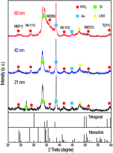
Fig. 1 shows the XRD patterns of the annealed HfO2 thin films of different thickness. Both monoclinic (M) and tetragonal (T) phase appear in the pattern. The coexistence of both phases in ALD-grown HfO2 films has also been described in other reports.23,24 The monoclinic phase is the most stable phase of HfO2 and has a lower dielectric constant, while the tetragonal phase has the highest dielectric constant. Therefore, the mixed phase structures may contribute to variations in the dielectric constant.18 The structures of the annealed HfO2 thin films were also investigated via Raman spectroscopy and X-ray photoelectron spectroscopy (XPS), which are shown in Fig. S1 and S2 of the ESI.† The peak positions and Hf 4f core level XPS conform to the obtained HfO2 films.Cross-sectional high-resolution transmission electron microscopy (HR-TEM) images of the HfO2 thin films prepared via ALD are shown in Fig. 2a. The fully crystalline nature of the HfO2 films is confirmed from the HR-TEM image and selected area electron diffraction (SAED) image, shown in the inset of Fig. 2a. Moreover, the interface between HfO2 and LNO can be distinguished. To further investigate the interface between the film and the substrate, a precise mapping of the elemental distribution was conducted via X-ray energy dispersive spectrometry, as shown in Fig. 2b–f. The diffusion between the bottom electrodes can be observed, i.e., Hf, La, Ni and Pt can cross the interface and enter the adjacent layers, which may occur during the thermal ALD process and annealing process. Moreover, a strange interdiffusion phenomenon of Hf and Pt elements can be clearly seen in Fig. 2c and f. From the Pt mapping image by the contrast, it was found that Pt tends to diffuse into the HfO2 layer rather than the neighboring LNO layer. This effect is hardly explained by the diffusion model during the annealing process. We linked this phenomenon to the fact that the Pt is more liable to migrate through LNO and combine with Hf. The same situation also takes place for the Hf that diffuses through the LNO layer and prefers to combine with the Pt layers. The impurities in the HfO2 layers may lead to annealed multiphase HfO2 films and contribute to the variation in the dielectric constant for HfO2 films of different thickness in this study. In short, the diffusion mechanisms among the HfO2 films, bottom electrodes and substrate are still under investigation.
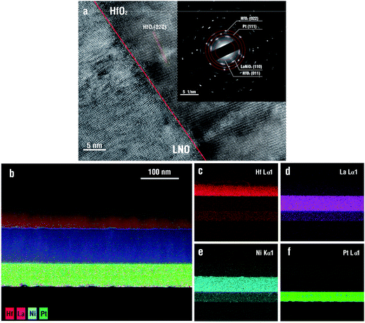 | ||
| Fig. 2 (a) HR-TEM images of HfO2; the inset shows the SAED pattern; (b–f) elemental mapping of the sample. | ||
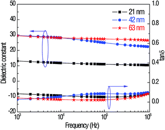
The frequency dependence of the dielectric properties is plotted in Fig. 3. The dielectric constant decreases when the frequency increases, indicating that some polarization mechanisms cannot make respond at high frequencies. The lower dielectric constant of the 21 nm HfO2 film compared with that of the 43 nm and 63 nm films may be attributed to the diffusion of Pt ions into the HfO2 layer, as shown in Fig. 2. The effect of using Pt directly as the bottom electrode on the dielectric properties of electrostatic capacitors had already been studied by researchers,25,26 and the conclusion was that a buffer layer such as LaNiO3 is needed to prevent the diffusion from the Pt electrode layer to the dielectric layer. Without a buffering LaNiO3 layer, more Pt ions could diffuse into the thinner dielectric layer during the same thermal ALD process and annealing process, which made the dielectric constant of 21 nm HfO2 films deteriorate greatly. Moreover, the dielectric constant increases with the grain size, particularly when the grain size is reduced to a nanoscale level. The surface morphologies measured via AFM of all the samples are shown in ESI S3.† The grain size in 21 nm HfO2 films is about 32 nm, which is half the grain size of 42 nm and 63 nm films, determined by the grain number in the same length scale. The tendency of the dielectric constant to increase as the grain size increases has also been studied by other researchers.27,28 The maximum dielectric constant at 1 MHz is about 26 obtained for the 63 nm HfO2 films, which is comparable with that reported in the literature.29 The dielectric loss was maintained at a low level of below 0.1 in the measured frequency range for all the samples.
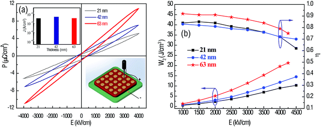
Fig. 4a and b shows the polarization–E-field (P–E) curves and the energy-storage properties calculated from the P–E curves of the HfO2 films with different thickness. All the samples exhibit typical linear dielectric P–E curves with a close-to-zero remanent polarization. Due to the maximal dielectric constant among the samples, the 63 nm HfO2 film offers a high polarization value at the same E-field, resulting in a high energy density. To exclude the effect of leakage current on the polarization, the thickness-dependent leakage current density J was measured, as shown in the inset of Fig. 4a. The J was determined to be as small as 3 × 10⁻⁷ to 6 × 10⁻⁷ A cm−2 for all the samples, indicating that the contribution of leakage current to polarization was negligible. The inset of Fig. 4a, at the bottom right corner, displays the schematic for the P–E test. Fig. 4b presents the recoverable energy density W2 and energy efficiency η at room temperature for all the HfO2 films measured from 1000 kV cm−1 to their critical breakdown strength at 10 kHz. It is found that W2 increases with E and reaches the maximum value at the breakdown strength. As is expected, the maximum W2 = 21.3 J cm−3 is achieved in the 63 nm HfO2 films at the breakdown strength with a relative high η = 75%. These results are comparable with those of nanocapacitors for energy storage, for example, a novel structure of TiN/Al2O3/TiN nanocapacitors on AAO were reported by Banerjee et al. The theoretical W2 of Al2O3 (εr ≈ 9) is estimated to be 4.6 J cm−3 at an identical E-field.30 Park et al. reported that the energy density of Hf0.3Zr0.7O2 AFE films with thickness of 29 nm at 4000 kV cm−1 was about 23 J cm−3.10 In addition, the maximum W2 values for 21 nm and 42 nm HfO2 films are 10.3 J cm−3 and 14.5 J cm−3, respectively, which are close to the reported value for traditional PZT-based AFE materials. As previously discussed, the most prominent advantage of linear dielectric energy storage materials compared to AFE/FE materials is their higher energy efficiency. The minimum η value of 62% observed in 21 nm HfO2 films at 4500 kV cm−1 is distinctly superior to that of AFE/FE materials at such a high E-field.
The temperature stability of the energy-storage performance is another important criterion for electrostatic capacitors and therefore, the thermal stability of the 63 nm capacitor was examined. Fig. 5a shows the P–E loops of the 63 nm films at a temperature range from 30 °C to 150 °C, measured at 3000 kV cm−1 and 10 kHz. The polarization of the films is mostly maintained constant at temperatures below 110 °C. Nevertheless, it drops as temperature increases. The inset in Fig. 5a shows a magnified picture of the P–E loops at different temperatures. The variation tendency of the polarization with the increasing temperature at a constant E-field is strongly related to the electrocaloric effect.31 According to the Maxwell's relation in thermodynamics:
 | (3) |
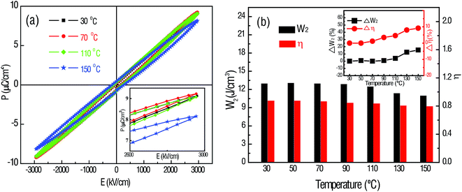 | ||
| Fig. 5 (a) Temperature-dependent P–E hysteresis loops of the 63 nm HfO2 thin films. (b) Temperature-dependent recoverable energy density and efficiency of the 63 nm HfO2 thin films. | ||
4. Conclusion
In summary, the energy-storage performance of the linear dielectric HfO2 films obtained via ALD method with different thickness was studied. The results show that HfO2 capacitors not only have larger recoverable energy densities than that of traditional AFE/FE material-based capacitors, but also possess much higher energy efficiencies. The maximum W2 = 21.3 J cm−3 was achieved in the 63 nm HfO2 film at 4250 kV cm−1 with a higher η = 75%. In addition, when an E-field of 3000 kV cm−1 was applied, the 63 nm HfO2 still exhibited a great energy-storage stability in the temperature range from room temperature to 150 °C. These results indicate that linear dielectric HfO2 thin films will be a great candidate for energy-storage devices.Acknowledgements
The work was supported by the Natural Science Foundation of China (Grant No. 51472199, 11534015, 51602244), Natural Science Foundation of Shaanxi Province (Grant No. 2015JM5196), the National 111 Project of China (B14040), the 973 Program (Grant No. 2015CB057402) and the Fundamental Research Funds for the Central Universities. The authors appreciate the support from the International Joint Laboratory for Micro/Nano Manufacturing and Measurement Technologies.References
- D. Larbalestier, A. Gurevich, D. M. Feldmann and A. Polyanskii, Nature, 2001, 414, 368–377 CrossRef CAS PubMed
.
- F. Bonaccorso, L. Colombo, G. Yu, V. Tozzini, A. C. Ferrari, R. S. Ruoff and V. Pellegrini, Science, 2015, 347, 1246501–1246509 CrossRef PubMed
.
- E. Frackowiak, K. Metenier, V. Bertagna and F. Beguin, Appl. Phys. Lett., 2015, 77, 2421–2423 CrossRef
.
- L. C. Haspert, E. Gillette, S. B. Lee and G. W. Rubloff, Energy Environ. Sci., 2013, 6, 2578–2590 CAS
.
- K. Yao, S. Chen, M. Rahimabady, M. S. Mirshekarloo, S. Yu, F. E. Hock Tay, T. Sritharan and L. Lu, IEEE Trans. Ultrason. Eng., 2011, 58, 1968–1974 CrossRef PubMed
.
- P. Banerjee, I. Perez, L. Henn-Lecordier, S. B. Lee and G. W. Rubloff, Nat. Nanotechnol., 2009, 4, 292–296 CrossRef CAS PubMed
.
- J. Vetter, P. Novak, M. R. Wagner, C. Veit, K. C. Moller, J. O. Besenhard, M. Winter, M. Wohlfahrt-Mehrens, C. Vogler and A. Hammouche, J. Power Sources, 2005, 147, 269–281 CrossRef CAS
.
- V. Etacheri, R. Marom, R. Elazari, G. Salitra and D. Aurbach, Energy Environ. Sci., 2011, 4, 3243–3262 CAS
.
- S. W. Kim, D. H. Seo, X. Ma, G. Ceder and K. Kang, Adv. Energy Mater., 2012, 2, 710–721 CrossRef CAS
.
- M. H. Park, H. J. Kim, Y. J. Kim, T. Moon, K. D. Kim and C. S. Hwang, Adv. Energy Mater., 2014, 4, 1400610–1400617 CrossRef
.
- X. H. Hao, Y. Wang, L. Zhang, L. W. Zhang and S. L. An, Appl. Phys. Lett., 2013, 102, 163903 CrossRef
.
- X. L. Wang, L. Zhang and X. H. Hao, Mater. Res. Bull., 2015, 65, 73–79 CrossRef CAS
.
- Z. S. Xu, X. H. Hao and S. L. An, J. Alloys Compd., 2015, 639, 387–392 CrossRef CAS
.
- B. L. Peng, Q. Zhang, X. Li, T. Y. Sun, H. Q. Fan, S. M. Ke, M. Ye, Y. Wang, W. Lu, H. B. Niu, J. F. Scott, X. R. Zeng and H. T. Huang, Adv. Electron. Mater., 2015, 1, 1500052 CrossRef
.
- T. M. Correia, M. McMillen, M. K. Rokosz, P. M. Weaver, J. M. Gregg, G. Viola and M. G. Cain, J. Am. Ceram. Soc., 2013, 96, 2699–2702 CrossRef CAS
.
- B. J. Chu, X. Zhou, K. L. Ren, B. Ness, M. R. Lin, Q. Wang, F. Bauer and Q. M. Zhang, Science, 2006, 313, 334–336 CrossRef CAS PubMed
.
- Z. C. Zhang, Q. J. Meng and T. C. M. Chung, Polymer, 2009, 50, 707–715 CrossRef CAS
.
- M. H. Park, H. J. Kim, Y. J. Kim, W. Lee and C. S. Hwang, Appl. Phys. Lett., 2013, 102, 242905–5 CrossRef
.
- C. V. Ramana, M. Noor-A-Alam, J. J. Gengler and J. G. Jones, ACS Appl. Mater. Interfaces, 2012, 4, 200–204 CAS
.
- T. Usui, C. A. Donnely, M. Logar, R. Sinclair, J. Schoonman and F. B. Prinz, Acta Mater., 2013, 61, 7660–7670 CrossRef CAS
.
- L. Y. Liang, H. T. Cao, Q. Liu, K. M. Jiang, Z. M. Liu, F. Zhuge and F. L. Deng, ACS Appl. Mater. Interfaces, 2014, 6, 2255–2261 CAS
.
- K. Kukli, T. Pilvi, M. Ritala, T. Sajavaara, J. Lu and M. Leskela, Thin Solid Films, 2005, 491, 328–338 CrossRef CAS
.
- J. H. Choi, Y. Mao and J. P. Chang, Mater. Sci. Eng., A, 2011, 72, 97–136 Search PubMed
.
- T. Wang and J. G. Ekerdt, Chem. Mater., 2009, 21, 3096–3101 CrossRef CAS
.
- D. H. Bao, N. Wakiya, K. Shinozaki, N. Mizutani and X. Yao, Appl. Phys. Lett., 2001, 78, 3286 CrossRef CAS
.
- X. H. Hao, J. W. Zhai and X. Yao, J. Cryst. Growth, 2008, 311, 90–94 CrossRef CAS
.
- C. L. Fu, H. W. Chen, L. Y. Hu, W. Cai and C. R. Yang, Integr. Ferroelectr., 2007, 92, 114–122 CrossRef CAS
.
- W. L. Shu, J. Wang and T.-Y. Zhang, J. Appl. Phys., 2012, 112, 064108 CrossRef
.
- F. M. Li, B. C. Bayer, S. Hofmann, S. P. Speakman, C. Ducati, W. I. Milne and A. J. Flewitt, Phys. Status Solidi B, 2013, 250, 957–967 CrossRef CAS
.
- P. Banerjee, I. Perez, L. Henn-Lecordier, S. B. Lee and G. W. Rubloff, ECS Trans., 2009, 25, 345–353 CAS
.
- A. S. Mischenko, Q. Zhang, J. F. Scott, R. W. Whatmore and N. D. Mathur, Science, 2006, 311, 1270–1271 CrossRef CAS PubMed
.
Footnote |
| † Electronic supplementary information (ESI) available. See DOI: 10.1039/c6ra27847g |
| This journal is © The Royal Society of Chemistry 2017 |

