 Open Access Article
Semiconducting properties of perchlorate-doped graphene using an electrochemical method†
Chang-Soo Parka,
Dongil Chu a,
Yoon Shonb and
Eun Kyu Kim
 *a
*a
aDepartment of Physics and Research Institute for Natural Science, Hanyang University, Seoul 133-791, Republic of Korea. E-mail: ek-kim@hanyang.ac.kr; Tel: +82 2 2220 4405
bQuantum Functional Semiconductor Research Center, Dongguk University, Seoul 100-715, Republic of Korea
First published on 16th March 2017
Abstract
We report a band gap opening and p-type doping for single layer graphene by an electrochemical method. The chlorine oxide doping to graphene was carried out in 0.1 M LiClO4/acetonitrile solution. The temperature dependent conductivity of the p-type doped graphene at an applied potential of 1.5 V during the electrochemical doping process showed the band gap of 0.094 eV.
Graphene, a two-dimensional carbon material, has attracted much attention due to its unique electrical and physical properties1 which can promise a variety of fundamental research opportunities and applications. However, graphene is a semimetal with a linear energy-momentum dispersion relation1 without a band gap. Recently, several researchers have tried to open a band gap in graphene by means of symmetry breaking, which induces a change in band structure. For instance, defect generation,2 molecular doping,3,4 applied bias,5–7 and nano ribbon,8 have shown band gap opening in graphene. More recently, boron-doped graphene by reactive microwave plasma showed tunable band gap engineering up to 0.54 eV.4 Even though the above mentioned result is close to adequate values for device applications, a more facile and precise control for the band gap tuning of the graphene is still desired to realize device applications. In general, the carbon atoms in the carbon nanotubes (CNTs) or in graphene are sp2 hybridized and they also have an unsaturated dangling bond, which can promise various surface modifications. Herein, we report a band gap opening and p-type semiconducting property of graphene using electrochemical doping on the graphene surface. Among electrolytes, LiClO4 is decomposed into Li+ + ClO4− by applied bias. Then, chlorine oxide (perchlorate) can easily combine with the unsaturated dangling bond in graphene during electrochemical doping. Furthermore, the amounts of doping can be controlled by electric potential. The perchlorate nanoparticles adsorbed on graphene were used as the dopants in an electrolyte, which induces the band gap opening and the change in the electronic structure.
The graphene used in this study was synthesized by chemical vapour deposition (see ESI†), and the graphene film for the working electrode was prepared to carry out the electrochemical redox reaction in the electrolyte solution (Fig. S1†). In general, the core of the experimental setup used in electrochemical doping is a typical 3-electrode electrochemical cell. The components of the cell include a working electrode, an auxiliary or counter electrode, and a reference electrode all submerged in the electrolyte solution. The electrochemical experiment was carried out using WPG potentiostats with Pt counter electrode and Ag/AgCl reference electrode. The electrochemical cell was equipped with a common glass beaker. The electrochemical doping was carried out in a 0.1 M LiClO4/acetonitrile solution, and the amount of adsorption of ClO4− for the doping was controlled using an electric potential between the reference and the working electrode. The higher the potential, the more concentration was adsorbed on graphene.9 In this study, we chose an optimized condition, where we used an applied potential of 1.5 V for perchlorate adsorption, and ClO4− ions were simultaneously doped on the surface of graphene. The film was rinsed in DI-water and outgassed at 80 °C in a vacuum oven after electrochemical doping in solution. The electronic structure was investigated by X-ray photoelectron spectroscopy (XPS, ESCALAB 250 XPS spectrometer, VG Scientifics). Raman spectra of the graphene film were measured for excitation of 514.5 nm at room temperature using a Jobin-Yvon HR800UV spectrometer. The electrical transport was measured in order to confirm the semiconductor properties using a cryostat with He displex (Sumitomo).
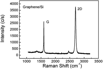
Fig. 1 shows the Raman spectra of the pristine single layer graphene film on Si after synthesis. All the areas of the sample showed a uniform Raman signal like that in Fig. 1. Two dominant peaks clearly appeared, including the G peak at ∼1592 cm−1 and the 2D peak at ∼2703 cm−1. The peak intensity ratios (I2D/IG) of pristine graphene are approximately less than two, while the full widths at half-maximum (FWHM) of the 2D peaks are about 32, indicating that this sample is, in fact, single layer graphene.10
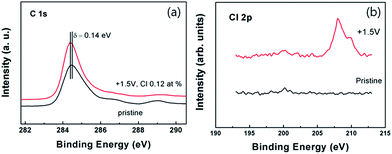
Fig. 2a shows representative C 1s spectra for graphene doped with perchlorate molecules. Detailed analysis of the XPS spectra provides clear evidence that graphene has been chemically modified. The peak position at 284.7 eV for pristine graphene without immersion in electrolyte is very close to the value for the pure sp2 C–C bonding in the pristine highly oriented pyrolytic graphite (HOPG), indicating that carbon atoms are almost exclusively sp2 hybridized in non-doped graphene.11 The perchlorate nanoparticles were adsorbed on graphene in a chemical bond by an unsaturated dangling bond or defect. The downshift of the carbon core level of 0.14 eV in the binding energy for graphene doped at 1.5 V evidences the p-type doping with the Fermi level change as the ClO4− ion adsorbe.12,13 The chlorine Cl 2p core level spectrum in graphene doped at 1.5 V, depicted in Fig. 2b, reveals clear doping. The atomic composition of doped graphene follows that of Cl, C, O, and Si at 0.12%, 68.9%, 24.5%, and 6.48%, respectively.
 | ||
| Fig. 2 XPS C 1s spectra of graphene doped with ClO4− ion at 1.5 V (a) and Cl 2p spectra of graphene doped at 1.5 V (b). | ||
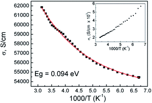
To obtain the transport properties of graphene, we measured the temperature dependence of conductivity. Fig. 3 shows the conductivity versus temperature plot of the perchlorate-doped graphene. The temperature-dependent conductivity was measured in the range from 150 to 300 K. The conductivity of the perchlorate-doped graphene increases with increasing temperature like a usual semiconductor and then can be fitted by the conductivity equation. However, the inset of Fig. 3 shows that the undoped graphene has a metallic behaviour. According to the previous study, the temperature-dependent conductivity of graphene at very low temperatures can be well explained by the variable range hopping (VRH) mechanism. However, thermally activated (TA) conduction is the main transport mechanism at high temperature, over 100 K. The TA model can be described as σ = σ0![[thin space (1/6-em)]](https://www.rsc.org/images/entities/char_2009.gif) exp(−Eg/2kT) for high temperature regions over 100 K.14,15 The observed band gap energy of the perchlorate doped graphene is determined to be 94 meV as shown in Fig. 3. Hence it induces the change of the electronic properties of materials. Therefore, the transition of electronic properties of graphene from semimetal to semiconductor in Fig. 3 is one of the strong evidences of chemical adsorption.
exp(−Eg/2kT) for high temperature regions over 100 K.14,15 The observed band gap energy of the perchlorate doped graphene is determined to be 94 meV as shown in Fig. 3. Hence it induces the change of the electronic properties of materials. Therefore, the transition of electronic properties of graphene from semimetal to semiconductor in Fig. 3 is one of the strong evidences of chemical adsorption.
 | ||
| Fig. 3 Temperature dependent conductivity of graphene doped with ClO4− ion. The inset shows the metallic behavior of undoped graphene. | ||
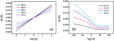
We fabricated back-gate FETs using the perchlorate-doped single layer graphene. Single layer graphene was formed after transfer onto a 300 nm-thick SiO2/Si substrate and used as a channel. A 50 nm gold layer deposited by e-beam evaporation was used as source and drain electrodes. The channel length was 10 μm, and the channel width was 100 μm. Fig. 4a shows I–V characteristics of the graphene FET device with various gate voltages. Fig. 4b shows I–V characteristics of the graphene FET device with various VDS at room temperatures. Herein, the I–V curve from the graphene FET clearly indicates a p-type semiconductor behavior. The field effect mobility of holes was determined by estimating the linear region of I–V curves using the equation μ = (L/WCoxVd)(ΔId/ΔVg) where, L and W are the channel length and width, respectively, and Cox is the gate capacitance for the 300 nm-thick SiO2. The field effect mobility was calculated to be 2406 cm2 V−1 s−1 for the perchlorate-doped graphene.
 | ||
| Fig. 4 (a) I–V characteristics of the perchlorate doped graphene FET device with various gate voltages. (b) I–V characteristics of the perchlorate doped graphene FET device with various VDS. | ||
Conclusions
In conclusion, we demonstrated the band gap opening and p-type graphene field effect transistor. The perchlorate-doped graphene has a shift of 0.14 eV in binding energy of XPS after doping. The temperature dependent conductivity indicates that the perchlorate doped graphene has a band gap of 94 meV. The fabricated back-gate graphene FET revealed a p-type semiconducting behavior. These results suggest a boosting of the band gap modulation for future graphene electronics.Acknowledgements
This study was supported in part by the National Research Foundation of Korea (NRF) grant funded by the Korea government (MSIP) (NRF-2016R1A2B4011706, 2016R1D1A1B03932295 and 2014R1A2A2A01007718).Notes and references
- K. S. Novoselov, A. K. Geim, S. V. Morozov, D. Jiang, M. I. Katsnelson, I. V. Grigorieva, S. V. Dubonos and A. A. Firsov, Nature, 2005, 438, 197 CrossRef CAS PubMed.
- X. Dong, Y. Shi, Y. Zhao, D. Chen, J. Ye, Y. Yao, F. Gao, Z. Ni, T. Yu, Z. Shen, Y. Huang, P. Chen and L.-J. Li, Phys. Rev. Lett., 2009, 102, 135501 CrossRef PubMed.
- T. Ohta, A. Bostwick, T. Seyller, K. Horn and E. Rotenberg, Science, 2006, 313, 951 CrossRef CAS PubMed.
- Y.-B. Tang, L.-C. Yin, Y. Yang, X.-H. Bo, Y.-L. Cao, H.-E. Wang, W.-J. Zhang, I. Bello, S.-T. Lee, H.-M. Cheng and C.-S. Lee, ACS Nano, 2012, 6, 1970 CrossRef CAS PubMed.
- E. Rudberg, P. Salek and Y. Luo, Nano Lett., 2007, 7, 2211 CrossRef CAS PubMed.
- Y.-W. Son, M. L. Cohen and S. G. Louie, Nature, 2006, 444, 347 CrossRef CAS PubMed.
- Y. Zhang, T.-T. Tang, C. Girit, Z. Hao, M. C. Martin, A. Zettl, M. F. Crommie, Y. R. Shen and F. Wang, Nature, 2009, 459, 820 CrossRef CAS PubMed.
- M. Y. Han, B. Ozyilmaz, Y. Zhang and P. Kim, Phys. Rev. Lett., 2007, 98, 206805 CrossRef PubMed.
- C. S. Park, Y. Zhao, J. H. Lee, D. M. Hwang, Y. Shon, Y. H. Song and C. J. Lee, Appl. Phys. Lett., 2013, 102, 032106 CrossRef.
- A. C. M. Ferrari, J. C. Meyer, V. Scardaci, C. Casiraghi, M. Lazzeri, F. Mauri, S. Piscanec, D. Jiang, K. S. Novoselov, S. Roth and A. K. Geim, Phys. Rev. Lett., 2006, 97, 187401 CrossRef CAS PubMed.
- S. Maldonado, S. Morin and K. J. Stevenson, Carbon, 2006, 44, 1429 CrossRef CAS.
- U. Dettlaff-Weglikowska, V. Skakalova, R. Graupner, S. H. Jhang, B. H. Kim, H. J. Lee, L. Ley, Y. W. Park, S. Berber, D. Tomanek and S. Roth, J. Am. Chem. Soc., 2005, 127, 5125 CrossRef CAS PubMed.
- T. Nagata, O. Bierwagen, M. E. White, M. Y. Tsai, Y. Yamashita, H. Yoshikawa, N. Ohashi, K. Kobayashi, T. Chikyow and J. S. Speck, Appl. Phys. Lett., 2011, 98, 232107 CrossRef.
- H. Miyazaki, K. Tsukagoshi, A. Kanda, M. Otani and S. Okada, Nano Lett., 2010, 10, 3888 CrossRef CAS PubMed.
- C.-S. Park, Y. Zhao, Y. Shon, I. T. Yoon, C. J. Lee, J. D. Song, H. Lee and E. K. Kim, J. Mater. Chem. C, 2015, 3, 4235 RSC.
Footnote |
| † Electronic supplementary information (ESI) available. See DOI: 10.1039/c7ra00332c |
| This journal is © The Royal Society of Chemistry 2017 |

