
 Open Access Article
 This Open Access Article is licensed under a
 Creative Commons Attribution 3.0 Unported Licence
Electrode buffer layers producing high performance nonvolatile organic write-once-read-many-times memory devices
Zhiguo Kongab,
Dongxue Liuab,
Jinghan Hea and
Xiuyan Wang *ab
*ab
aKey Laboratory of Preparation and Applications of Environmental Friendly Materials (Jilin Normal University), Ministry of Education, Changchun 130103, China. E-mail: wangxiuyanjlnu2004@163.com
bDepartment of Chemistry, Jilin Normal University, Siping 136000, China
First published on 24th February 2017
Abstract
CuI and Bphen are adopted as the electrode buffer layers for a PbPc/F16CuPc heterojunction based nonvolatile organic write-once-read-many-times memory device, which improve the ON/OFF ratio up to one order of magnitude while significantly reducing the threshold voltage compared to the non-buffer-layer counterpart.
Organic resistive memory devices have attracted a lot of attention due to their simple device structure, good scalability, low-cost, low-power consumption, large data storage capacity, and high cycling endurance.1–5 Depending on their memory characteristics, organic memory devices can be simply classified into three types: random access memory, read-write-erase-rewritable memory, and write-once-read-many-times (WORM) memory. Among these memory devices, WORM memory is an important type of nonvolatile memory which can hold data permanently and be read from repeatedly. WORM memory devices have been extensively investigated due to their potential applications for wireless identification tags, smart cards, and personal data depositories. A typical organic resistive memory device usually has a sandwich structure where the switchable organic material is inserted between two electrodes. Organic switchable materials used for these devices range from small molecular materials to polymers and organic/inorganic composites. Correspondingly, a lot of mechanisms have been proposed to account for the transition between the high conductivity (ON) and low conductivity (OFF) states, for example, charge carrier trapping and detrapping,6–8 filament formation and destruction,9,10 conformation change,11 oxidation/reduction reaction,12,13 and charge-transfer complex formation.14,15
Recently, Wang et al. have demonstrated that the interfacial dipole layer in an indium tin oxide (ITO)/hexadecafluoro-copper-phthalocyanine (F16CuPc) interface and copper phthalocyanine (CuPc)/F16CuPc interfaces can control the conductivity state of WORM memory devices.16,17 Meanwhile, a high ON/OFF current ratio in the order of 104 is achieved in the CuPc/F16CuPc heterojunction based device.17 However, the switch threshold voltage of this device is about −8 V. Such a high switch threshold voltage is not economical from the energy consumption point of view. Lead phthalocyanine (PbPc) is a member of the metal phthalocyanine family with the similar chemical and physical stability to CuPc, and it has been applied for organic solar cells18–20 and photodetectors.21–23 On the other hand, electrode buffer layer has been widely adopted in organic electronic devices, such as organic light-emitting diodes and organic solar cells.24 The introduction of buffer layer can alter the energy level alignment, material growth pattern, and chemical reaction in the interface. Improved performance has been demonstrated in organic light-emitting diodes and organic solar cells by using suitable electrode buffer layer. However, such a strategy has not been exploited in organic memory devices.
In this work, nonvolatile organic WORM memory devices based on PbPc/F16CuPc heterojunction has been demonstrated. The PbPc/F16CuPc bilayer heterojunction WORM memory device shows a high switch threshold voltage of −4.4 V and a low ON/OFF current ratio of 103. However, by inserting CuI and 4,7-diphenyl-1,10-phenanthroline (Bphen) as the anode and cathode buffer layer, respectively, the device exhibits a low switch threshold voltage of −2.2 V and a high ON/OFF ratio in the order of 104.
ITO coated glass substrates with a sheet resistance of 15 Ω sq−1 were used as the substrates. These substrates were cleaned sequentially with deionized water, acetone, and ethanol in an ultrasonic bath. Before loading into the high vacuum chamber, they were treated in an ultraviolet-ozone environment for 15 min. All organic layers and Al cathode were deposited onto the substrates via thermal evaporation under a pressure of 5 × 10⁻⁴ Pa. The bilayer heterojunction device has a structure of ITO/PbPc (60 nm)/F16CuPc (60 nm)/Al (100 nm) (Device A). To improve the performance, a device with a structure of ITO/CuI (4 nm)/PbPc (60 nm)/F16CuPc (60 nm)/Bphen (5 nm)/Al (100 nm) (Device B) was also fabricated, as shown in Fig. 1 with the energy level data from reports.18,25–27 The top Al cathode was deposited through a shadow mask and the area of the devices is 3 × 3 mm2 defined by the overlap of ITO and Al electrodes. Deposition rates and thickness of the layers were monitored in situ using oscillating quartz monitors. The evaporating rates were kept at 1 Å s−1 for CuI and organic layers and 10 Å s−1 for Al cathode, respectively. Current–voltage (J–V) characteristics of the devices were measured with a Keithley 2400 sourcemeter. The measurements were carried out at room temperature under ambient conditions without encapsulation.
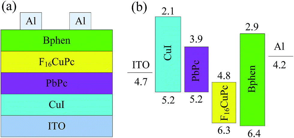 | ||
| Fig. 1 (a) Structure and (b) schematic energy level diagram of Device B. | ||
Fig. 2 shows the J–V curves of Device A with different voltage sweep directions. It can be found that it is on its ON state for the first voltage sweep and the first stage of the second voltage sweep. For the second voltage sweep, the current decreases with the increase of negative voltage after the voltage higher than −4.4 V, indicating that a distinct negative differential resistance (NDR) region appears. This suggests that the device transits from ON state to OFF state. Such a transition corresponds to the “writing” process of a digital memory cell. It should be pointed out that the switch threshold voltage (−4.4 V) is dramatically lower than that reported in the device based on CuPc/F16CuPc heterojunction (−7.6 V).17 This indicates that the device may be more favorable for application in low-power-consumption memory device. After this voltage sweep, the device is permanently turned to its OFF state for the latter voltage sweeps in both the positive and negative voltage regions (the third and forth voltage sweeps), and it cannot be recovered to ON state again even a high voltage of ±20 V is applied to this device. These properties suggest that it can be used as a WORM memory device. However, the maximum ON/OFF current ratio of this device in positive and negative voltage regions is only about 103 and 10, respectively. Such a character is insufficiently for practical applications.
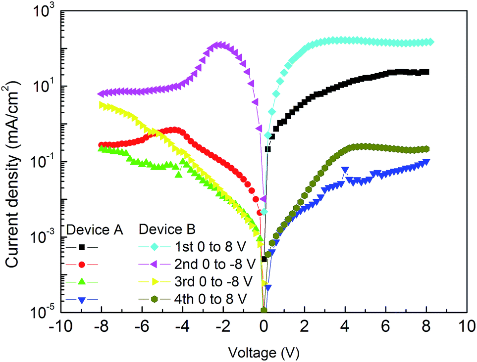 | ||
| Fig. 2 J–V curves of the devices with (Device B) and without (Device A) electrode buffer layers. | ||
A higher ON/OFF ratio of the device can be expected if the ON state current of the device were increased and/or the OFF state current were decreased. To satisfy these hypotheses, CuI and Bphen are adopted as the anode and cathode buffer layers, respectively. Fig. 2 shows the J–V curves of this device (Device B). Similar WORM memory properties are found in Device B. It can be found that both the OFF state currents at positive and negative voltage regions are little affected by the buffer layers, especially at lower voltage. However, both the ON state currents at positive and negative voltage regions are dramatically increased. Fig. 3 illuminates the ON/OFF current ratio of Device B in both positive and negative voltage regions. It can be found that the maximum ON/OFF current ratios in both positive and negative voltage regions can reach up to the order of 104, which are comparable to that in CuPc/F16CuPc based WORM memory device reported by Wang et al.17 The significant boosted ON/OFF ratio is primary attributed to the increased ON state current. Besides, the ON/OFF current ratio of Device B is higher than 103 in a large voltage region. This would significantly eliminate the memory error and elevate the reliability of the device for practical applications.
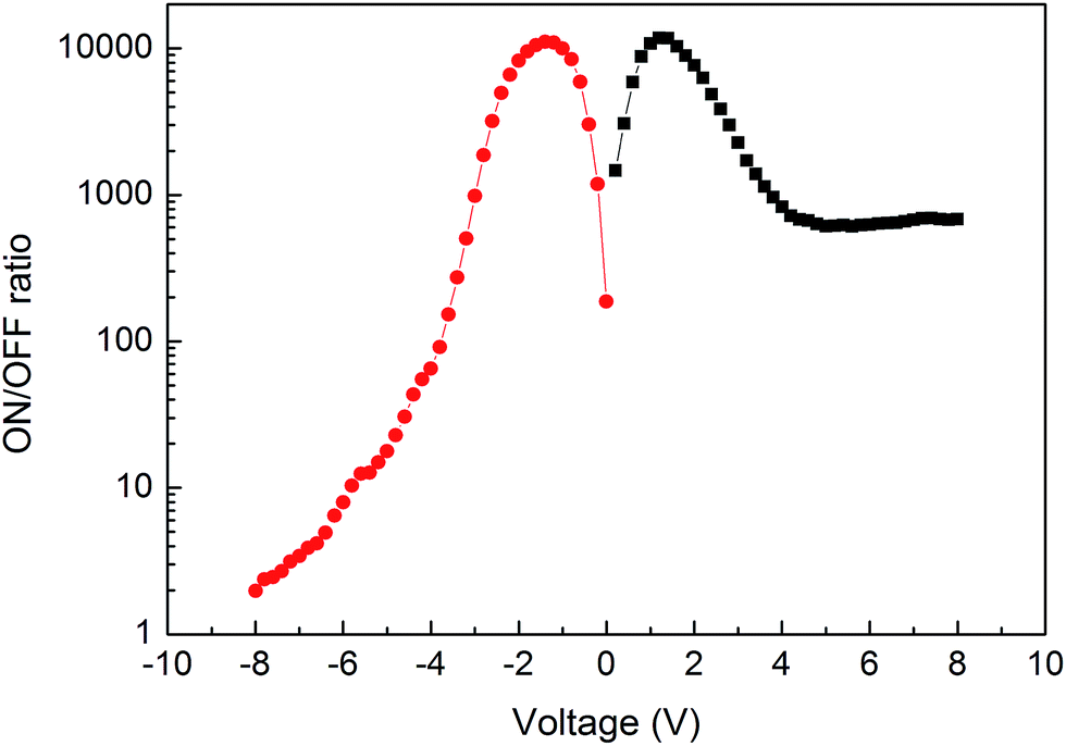 | ||
| Fig. 3 ON/OFF current ratio of Device B in positive and negative voltage regions. | ||
More interesting, it can be found from Fig. 2 that the switch threshold voltage is −2.2 V for Device B, which is only half to that of Device A. This indicates that Device B can be operated at a lower voltage, which can reduce the power consumption of the memory device. We have fabricated 8 devices in the same batch, and all these devices display obvious WORM memory characters. The switch threshold voltage and ON/OFF ratio of these devices vary from −2.0 to −2.8 V and 6 × 10³ to 1.4 × 10⁴, respectively, indicating high reproducibility of these devices. Resistance transition of a memory device is related to either the bulk or the interfacial properties. In view of that both Devices A and B exhibit WORM memory properties, it can be concluded that the WORM memory of these devices is not related to the interfaces of ITO/PbPc, ITO/CuI, CuI/PbPc, F16CuPc/Bphen, F16CuPc/Al, and Bphen/Al.
To further understand the mechanism of the devices, another device with a structure of ITO/PbPc/Bphen/F16CuPc/Al (Device C) was fabricated. Surprisingly, no conductivity transition is observed in this device. This suggests that the bulk properties of PbPc and F16CuPc related mechanisms, such as charge carrier trapping and detrapping, can be ruled out. Thus we come to the conclusion that the WORM memory of Devices A and B is related to the interfacial property of PbPc/F16CuPc. These can well explain that no conductivity transition is observed in Device C as there is no direct contact between PbPc and F16CuPc.
In the CuPc/F16CuPc based WORM memory device, the working mechanism was attributed to the interfacial dipole layer formation in the CuPc/F16CuPc interface.17 In view of that PbPc has an analogous molecular structure and similar energy level to that of CuPc, we propose that the WORM memory characters are related to the PbPc/F16CuPc interfacial dipole layer formed with the direction from PbPc to F16CuPc due to electron transfer from PbPc to F16CuPc. The energy barriers for hole and electron injection from Al and ITO electrodes are 2.2 and 2.6 eV, respectively, when judging from the schematic energy level diagram of the device shown in Fig. 1(b), which are higher for hole and electron injections. However, the formatted interfacial dipole layer at PbPc/F16CuPc interface may form a space electrical field in the device, which will reduce the charge carrier injection barriers.
It has been reported that a dipole layer is found in the ITO/CuI interface due to electron transfer from ITO to CuI, which increases the workfunction of ITO surface by about 0.7 eV.28 On the other hand, Shen et al. have demonstrated that a strong chemical reaction occurs between F16CuPc and Al during the thermally evaporation of Al cathode, which forms an insulating (F16CuPc)3Al layer.29 Thus the higher ON state currents at both positive and negative voltage of Device B can be attributed to the improved charge carrier injection from the electrodes due to the inserting of CuI and Bphen buffer layers. This suggests that the electrode buffer layers are essential for resistive memory devices to tune the carrier injection property. However, such a role has not been exploited in previous reports.
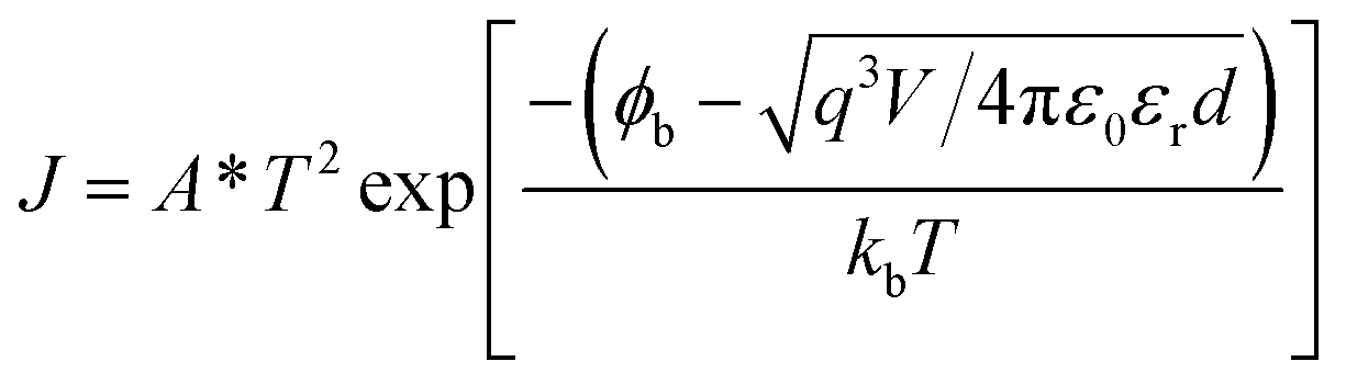
To further confirm the conduction mechanisms of the WORM device, the J–V characteristics of Device B are fitted with different current transport models. It can be found that a linear relation between log![[thin space (1/6-em)]](https://www.rsc.org/images/entities/char_2009.gif) J and V1/2 is observed in both the ON and OFF states current at low positive voltage, as shown in Fig. 4(a), where the currents subject to the Schottky emission model with the equation of:
J and V1/2 is observed in both the ON and OFF states current at low positive voltage, as shown in Fig. 4(a), where the currents subject to the Schottky emission model with the equation of:
 | (1) |
J and logV is found for both the ON and OFF states current at high positive voltage, as shown in Fig. 4(b). This implies that the current is bulk transport limited and complies with a trap-limited space charge limited current (SCLC) model with the equation of:
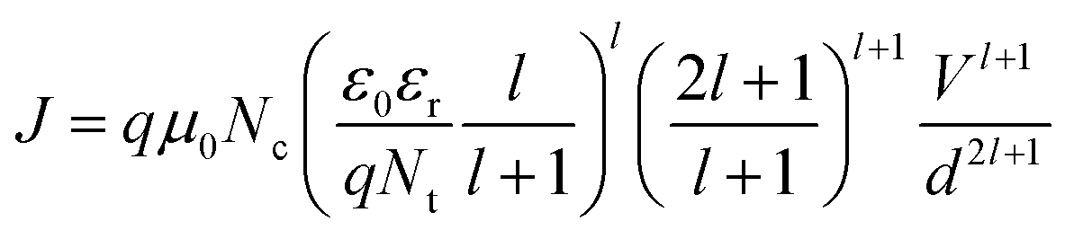 | (2) |
 | ||
| Fig. 4 (a) J verses V1/2 plots of ON and OFF states current of Device B at positive voltage. (b) Log–log plots of the ON and OFF states current of Device B at positive voltage. The lines present the linear fitting of the data. | ||
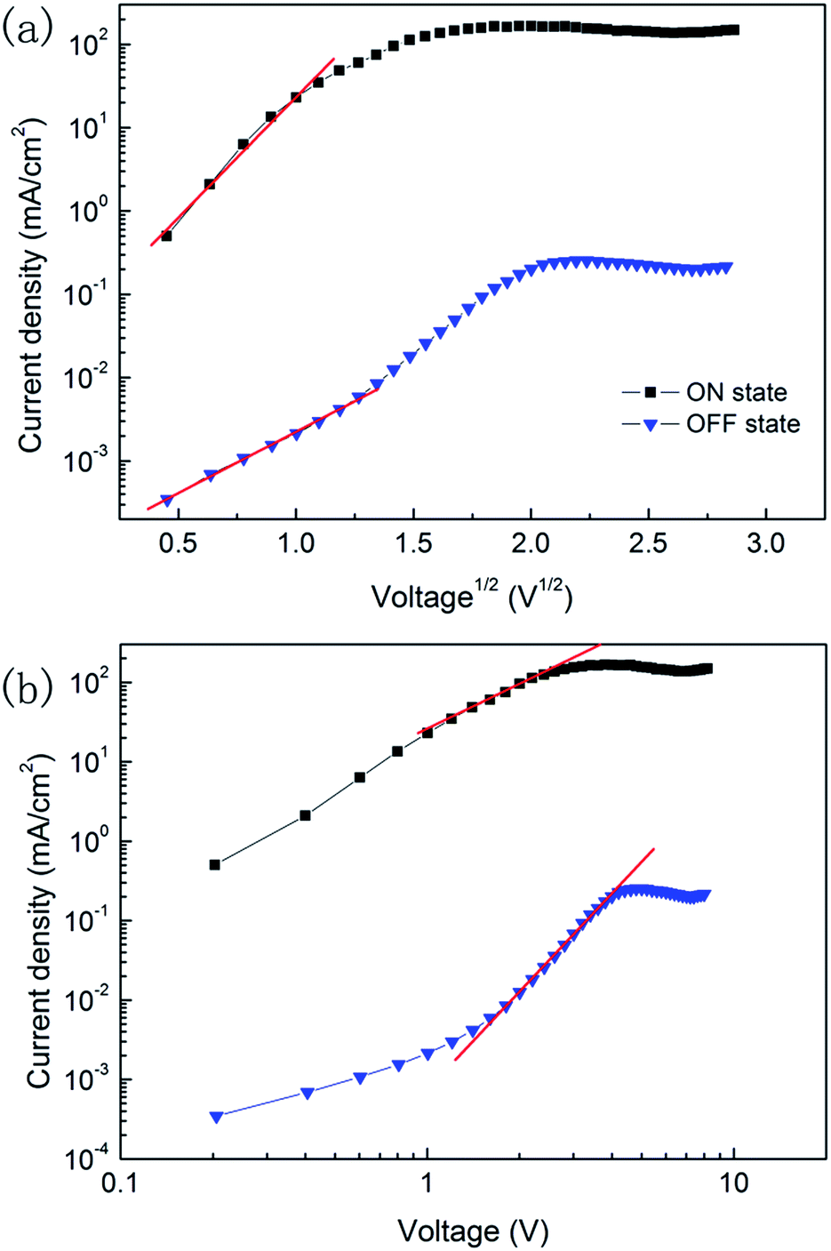
The ON state current in negative voltage before conductivity transition also shows a linear relation between logJ and log|V|, indicating that it obeys the trap-limited SCLC model, as shown in Fig. 5. This finding indicates that the ON state current at negative voltage is not injection but bulk transport limited. Such a character reverses the charge carrier injection barriers as found in Fig. 1(b) if only the energy levels of the materials were concerned. However, this can be well understood if we take the PbPc/F16CuPc interfacial dipole layer into account. The interfacial dipole layer would lower the hole and electron injection barriers from the Al cathode and ITO anode, respectively, as discussed before.
 | ||
| Fig. 5 Log–log plot of the ON state current of Device B at negative voltage, the line presents the linear fitting of the data. | ||
After the device transition from the ON state to OFF state, the interfacial dipole layer of PbPc/F16CuPc is destructed. Then the current transient from bulk limited to injection limited. In term of the large carrier injection barriers under negative bias, the current should follow the tunnelling model. If the shape of the tunnel barrier were trapezoidal, then the current follows direct tunnelling model with the equation of:30,31
 | (3) |
 | (4) |
It can be found from Fig. 6 that a linear relation between ln(J/V2) and ln(|1/V|) is observed at low voltage, while between ln(J/V2) and |1/V| at high voltage. These indicate that the shape of the tunnel barrier is trapezoidal at low voltage, while it turns to triangular at high voltage. Thus the current model transits from a direct tunnelling model at low voltage to an F–N tunnelling model at high voltage.
 | ||
| Fig. 6 (a) A ln(J/V2) versus ln|1/V| plot and (b) ln(J/V2) versus |1/V| plot of the OFF state current of Device B. The lines present the linear fitting of the data. | ||
According to the results found above, the ON state of the device at positive voltage region is attributed to the lower charge carrier injection barrier due to the introduction of the electrode buffer layers, while the ON state at negative voltage is attributed to the interfacial dipole layer formed at PbPc/F16CuPc. The OFF state is attributed to the destruction of this interfacial layer and formation of an insulting layer. It should be noted that slight NDR regions are also found in the ON and OFF states at high voltage of positive voltage region, as shown in Fig. 2(b). This should also be attributed to a slight destruction of the interfacial dipole layer. At a low voltage, the injected holes and electrons are primarily recombination at the PbPc/F16CuPc interface. However, at a high voltage, more holes and electrons are injected, the excess holes or electrons will destroy the interfacial dipole layer.
It is found in Fig. 2 that the switch threshold voltage of Device B is lower that Device A and CuPc/F16CuPc based WORM device.17 For a WORM memory device with an interfacial dipole layer controlled resistive states, the switch threshold voltage depends on the strength of the interfacial dipole and/or the electrical filed across the interface. The electron injection barrier from ITO to PbPc is 0.8 eV (Fig. 1), while it is 1.6 eV from ITO to CuPc.17 From these energy levels, we cannot gain the reasons for the lower threshold voltage of Device B than CuPc/F16CuPc based WORM device. To address this issue, another device with the structure of ITO/CuI/PbPc/F16CuPc/Al (Device D) was fabricate. Although the electron injection barrier is increased to 2.6 eV from ITO, this device shows a switch threshold voltage of only −5.0 V, which is still lower than CuPc/F16CuPc based device. Such a lower switch threshold voltage may indicate that a lower strength of the PbPc/F16CuPc interfacial dipole than CuPc/F16CuPc, thus the interfacial dipole layer can be destroyed at a lower voltage. On the other hands, the lower switch threshold voltage of Device B than Device A can be attributed to a higher voltage across the PbPc/F16CuPc interface due to the introduced Bphen layer restricting the formation of (F16CuPc)3Al insulating layer. Similar result has been found in CuPc/F16CuPc based WORM device when a poly (ethylene oxide) cathode buffer layer was used.17 These findings suggest that the lower switch threshold voltage of Device B can be attributed to both the lower intrinsic strength of the PbPc/F16CuPc interfacial dipole and the higher voltage across the PbPc/F16CuPc interface. Still, substantial future experimental work is required to understand these phenomena and their mechanisms, especially the exact energy level alignment of the device before and after conductivity transition.
Retention stability is another figure-of-merit for memory devices. The ON and OFF states retention times of Device B are depicted in Fig. 7. Both the ON state and OFF state current densities were measured by applying a constant voltage of 0.5 V to the device. During the 1000 s time, the ON state current decreases from 1.6 to 0.9 mA cm−2, while the OFF state current only decreases from 5.7 × 10⁻⁴ to 5.3 × 10⁻⁴ mA cm−2, corresponding to a slight decrease of ON/OFF ratio from 2.8 × 10³ to 1.7 × 10³. More importantly, an ON/OFF ratio higher than 103 can also be achieved even after 104 s by tracing the evolution trend of the currents.
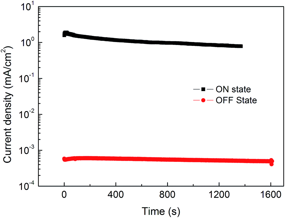 | ||
| Fig. 7 Retention stability of the ON and OFF states of Device B under bias of 0.5 V. | ||
Conclusions
In summary, a nonvolatile organic WORM memory device is demonstrated based on PbPc/F16CuPc heterojunction. By using CuI and Bphen as the anode and cathode buffer layers, the device shows a low switch threshold voltage of −2.2 V and a high ON/OFF current ratio in the order of 104 as well as a high retention stability. The lower switch threshold voltage can be attributed to both the lower intrinsic strength of the PbPc/F16CuPc interfacial dipole and the higher voltage across the PbPc/F16CuPc interface. These results suggest that the buffer layers play important roles in organic WORM memory devices, and this work provides a strategy to construct high performance and low-power-consumption nonvolatile organic WORM memory devices.Acknowledgements
This work was supported by the National Natural Science Foundation of China (Grant No. 21607051).Notes and references
- L. P. Ma, J. Liu and Y. Yang, Appl. Phys. Lett., 2002, 80, 2997 CrossRef CAS.
- Q. D. Ling, D. J. Liaw, E. Y. H. Teo, C. Zhu, D. S. H. Chan, E. T. Kang and K. G. Neoh, Polymer, 2007, 48, 5182 CrossRef CAS.
- C. Wang, P. Gu, B. Hu and Q. Zhang, J. Mater. Chem. C, 2015, 3, 10055 RSC.
- Z. S. Su, M. K. Fung, C. S. Lee, W. L. Li and S. T. Lee, Appl. Phys. Lett., 2008, 93, 083301 CrossRef.
- C. Wu, F. Li, Y. Zhang and T. Guo, Appl. Phys. Lett., 2012, 100, 042105 CrossRef.
- J. Jin and D. Ma, Org. Electron., 2009, 10, 275 CrossRef.
- Y. Ma, P. Y. Gu, F. Zhou, H. L. Dong, Y. Y. Li, Q. F. Xu, J. M. Lu and W. L. Ma, RSC Adv., 2015, 5, 7083 RSC.
- V. C. Nguyen and P. S. Lee, Sci. Rep., 2016, 6, 19594 CrossRef CAS PubMed.
- T. J. Whitcher, K. L. Woon, W. S. Wong, N. Chanlek, H. Nakajima, T. Saisopa and P. Songsiriritthigul, J. Phys. D: Appl. Phys., 2016, 49, 075104 CrossRef.
- I. Hattenhauer, F. A. D. Radomski, C. D. A. Duarte and M. A. Mamo, Org. Electron., 2016, 34, 57 CrossRef CAS.
- E. Y. H. Teo, Q. D. Ling, Y. Song, Y. P. Tan, W. Wang, E. T. Kang, D. S. H. Chan and C. Zhu, Org. Electron., 2006, 7, 173 CrossRef CAS.
- S. Möller, C. Perlov, W. Jackson, C. Taussig and S. R. Forrest, Nature, 2003, 426, 166 CrossRef PubMed.
- J. Wang, X. Cheng, M. Caironi, F. Gao, X. Yang and N. C. Greenham, Org. Electron., 2012, 12, 1271 CrossRef.
- Y. Song, Y. P. Tan, E. Y. H. Teo, C. Zhu, D. S. H. Chan, Q. D. Ling, K. G. Neoh and E. T. Kang, J. Appl. Phys., 2006, 100, 084508 CrossRef.
- B. Mukherjee and A. J. Pal, Chem. Mater., 2007, 19, 1382 CrossRef CAS.
- L. Wang, Z. Su and C. Wang, Appl. Phys. Lett., 2012, 100, 213303 CrossRef.
- L. Wang, Z. Su and C. Wang, Org. Electron., 2013, 14, 1163 CrossRef CAS.
- J. Dai, X. Jiang, H. Wang and D. Yan, Appl. Phys. Lett., 2007, 91, 253503 CrossRef.
- H. J. Kim, H. S. Shim, J. W. Kim, H. H. Lee and J. J. Kim, Appl. Phys. Lett., 2012, 100, 263303 CrossRef.
- F. Hou, F. Jin, B. Chu, Z. Su, Y. Gao, H. Zhao, P. Cheng, J. Tang and W. Li, Sol. Energy Mater. Sol. Cells, 2016, 157, 989 CrossRef CAS.
- X. Wang, H. Li, Z. Su, F. Fang, G. Zhang, J. Wang, B. Chu, X. Fang, Z. Wei, B. Li and W. Li, Org. Electron., 2014, 15, 2367 CrossRef CAS.
- X. Wang, F. Fang, Z. Su, X. Fang, G. Zhang, J. Wang, Z. Wei, J. Li and X. Wang, J. Phys. D: Appl. Phys., 2014, 47, 335104 CrossRef.
- Z. Su, F. Hou, X. Wang, Y. Gao, F. Jin, G. Zhang, Y. Li, L. Zhang, B. Chu and W. Li, ACS Appl. Mater. Interfaces, 2015, 7, 2529 CAS.
- H. Ishii, K. Sugiyama, E. Ito and K. Seki, Adv. Mater., 1999, 11, 605 CrossRef CAS.
- J. C. Bernède, L. Cattin, M. Makha, V. Jeux, P. Leriche, J. Roncali, V. Froger, M. Morsli and M. Addou, Sol. Energy Mater. Sol. Cells, 2013, 110, 107 CrossRef.
- C. Shen and A. Kahn, J. Appl. Phys., 2001, 90, 4549 CrossRef CAS.
- M. Y. Chan, C. S. Lee, S. L. Lai, M. K. Fung, F. L. Wong, H. Y. Sun, K. M. Lau and S. T. Lee, J. Appl. Phys., 2006, 100, 094506 CrossRef.
- C. H. Cheng, J. Wang, G. T. Du, S. H. Shi, Z. J. Du, Z. Q. Fan, J. M. Bian and M. S. Wang, Appl. Phys. Lett., 2010, 97, 083305 CrossRef.
- C. Shen, A. Kahn and J. Schwartz, J. Appl. Phys., 2001, 90, 6236 CrossRef CAS.
- J. M. Beebe, B. S. Kim, J. W. Gadzuk, C. D. Frisbie and J. G. Kushmerick, Phys. Rev. Lett., 2006, 97, 026801 CrossRef PubMed.
- B. K. Sarker and S. I. Khondaker, ACS Nano, 2012, 6, 4993 CrossRef CAS PubMed.
| This journal is © The Royal Society of Chemistry 2017 |