 Open Access Article
Creative Commons Attribution 3.0 Unported Licence
Transport properties of a three-shell icosahedral matryoshka cluster: a first-principles study†
Lu Zhanga,
Jing Huang*b,
Weiyi Wanga,
Qunxiang Li *a and
Jinlong Yang
 a
a
aHefei National Laboratory for Physical Sciences at the Microscale, Synergetic Innovation Center of Quantum Information and Quantum Physics, University of Science and Technology of China, Hefei, Anhui 230026, China. E-mail: liqun@ustc.edu.cn
bSchool of Materials and Chemical Engineering, Anhui Jianzhu University, Hefei, Anhui 230601, China. E-mail: jhuang@ustc.edu.cn
First published on 23rd February 2017
Abstract
Extensive efforts have been devoted to explore transport behaviors through various molecules and clusters, which are promising building blocks in molecular electronics. Here, we examine the spin-polarized electronic structures and transport properties of a three-shell icosahedral matryoshka cluster, Pb@Mn12@Pb20, by performing density functional theory calculations combining with non-equilibrium Green's function method. Theoretical results clearly reveal that, twelve Mn atoms in the middle layer anti-ferromagnetically couple with the center Pb atom and Pb atoms in the outlayer, while the Pb@Mn12@Pb20 cluster still has a huge magnetic moment of 28.0 bohr magneton, mainly contributed by these Mn atoms. The calculated spin-resolved transmission spectra of the proposed Pb@Mn12@Pb20 junctions exhibit robust spin filtering effect, which is not sensitive to the anchoring distance and the adopted electrode materials, and the conductance through the cluster under the small bias voltage is mainly determined by the spin-up electrons. These findings indicate that this kind of three-shell matryoshka cluster with huge magnetic moment holds potential applications in molecular spintronic devices.
1 Introduction
Since Aviram and Ratner first proposed the assumption of the molecular rectifier through a molecular junction in 1974,1 it took almost 20 years of technological developments to realize the first experiment resembling transport through single molecules. Fortunately, the field of molecular electronics has made significant progress in the past decades.2–4 Recently, combining the contemporary exploitation of the electron and spin degrees of freedom at single-molecule level, molecular spintronics has attracted considerable attention since it holds promise for the next generation of electronic devices with enhanced functionality and improved performance, and now it finds various applications in nanodevices, most notably in the logical and memory units of computers.4–10A variety of techniques, i.e. mechanical break junctions, electrochemical deposition, electromigration, electron beam lithography, shadow mask evaporation, scanning probe techniques, on-wire lithography and molecular rulers, have been developed to build molecular junctions,3,11 based on various promising candidates, such as organometallic wire,12–14 metal phthalocyanines,15,16 metal clusters,17–19 magnetic C28 molecule,20 and molecular magnets.21,22 Various spin devices including spin filtering, spin valves, and spin crossover, have been successfully demonstrated in experiments or have been theoretically predicted.23–25 Among various candidates, metal clusters have many special interesting controlled properties, which can be altered by the geometric structure, symmetry, cluster size, composition and the charged states. Previous investigations mainly focus on the physicochemical properties of metal clusters.26,27 For example, the magnetic moments of transition metal (TM)-doped Au6 cluster vary from 0 to 4.0 μB (Bohr magneton) by doping different TM atoms. The transport behavior of this kind of TM-doped clusters is limited so far. Our previous study has demonstrated that the spin-resolved transmission spectra of Mn@Au6 sandwiched between two Li(100) electrodes exhibit robust spin filtering effect.28 Clearly, more attention should be paid for their transport property.
Recently, several groups have proposed novel magnetic metal clusters,26,27,29,30 namely, three-shell icosahedral matryoshka clusters with the highest symmetry of Ih point group, which are promising building blocks in novel magnetic materials and devices since they have large magnetic moments, moderate HOMO–LUMO gaps, and weak inter-cluster interaction energies.29 Unfortunately, to our knowledge, their transport behaviors have not been visited so far. Previous reports mainly focused on the geometric structure, electronic and magnetic properties. Here, based on extensive density functional theory calculations combined with nonequilibrium Green's function formalism, we explore the spin-polarized transport properties through Pb@Mn12@Pb20 cluster. This three-shell icosahedral matryoshka cluster has a huge magnetic moment of 28.0 μB (Bohr magneton), mainly contributed by the Mn atoms, although the Mn atoms in the cluster anti-ferromagnetically couple with the Pb atoms in subunits. According to the calculated spin-resolved transmission spectra, we find that these Pb@Mn12@Pb20-based junctions exhibit robust spin filtering effect, and the conductance through the cluster is mainly determined by the spin-up electrons under the small bias voltage.
2 Computational methods
In our calculations, geometry optimizations, electronic structures and transport properties of Pb@Mn12@Pb20 cluster are calculated by using density functional theory calculations31 combined with non-equilibrium Green's function method, which is implemented in ATK package.32,33 The interaction between ionic cores and valence electrons is modeled with Troullier–Martins nonlocal pseudopotential. The generalized gradient approximation (GGA) in the PW91 form is used to describe the exchange and correlation energy,34 since the trends and predictions from DFT are clear and understandable at the PW91 level. An energy cutoff is set to be 150 Ry for the real-space grid on which the Poisson equation is solved. This is sufficient for electronic structure and transport calculations of Pb@Mn12@Pb20 cluster (see ESI†). Here, double-zeta plus polarization basis is used for all Pb and Mn atom in clusters, while single-zeta plus polarization basis is used for electrodes (i.e. Au and Cu) to save the computational cost.The spin-polarized transmission coefficients of these proposed molecular junctions are calculated by
| Tσ(E,V) = Tr[ΓLGσΓRG+σ]. | (1) |
 | (2) |
3 Results and discussion
3.1 Free Pb@Mn12@Pb20 cluster
We start with performing spin-polarized DFT calculations for the geometric, magnetic and electronic properties of the free Pb@Mn12@Pb20 cluster as benchmark. Fig. 1(a) shows the optimized structure. The most energy stable configuration of Pb@Mn12@Pb20 cluster displays a perfect icosahedral symmetrical three-shell matryoshka doll structure. It is an outer Pb20 regular dodecahedron encapsulating a Mn12 icosahedron, which in turn encapsulates a center Pb atom. Note that this cluster has icosahedral symmetry (Ih group), but its shape is not an icosahedron but a pentadodecahedron. The optimized Pb–Pb and Mn–Mn distances are about 3.29 and 2.75 Å, respectively. To determine the ground state of Pb@Mn12@Pb20 cluster, different magnetic configurations are examined, and we find that the calculated magnetic moments are not sensitive to the adopted functionals. The Pb@Mn12@Pb20 cluster prefers to the spin-polarized state, and the total magnetic moment (MM) is predicted to be 28.0 μB, while the atomic MM of Mn and Pb in the midderlayer and outlayer is about 3.49 and −0.64 μB, while the center Pb atom has −0.99 μB, respectively. Clearly, that the total MM is mainly contributed by the twelve Mn atoms, which anti-ferromagnetically couple with the center Pb atom and Pb atom in the outlay. Fig. 1(b) presents the spin density of Pb@Mn12@Pb20 cluster, here, the blue and yellow regions stand for the spin-up and spin-down densities, respectively. It is clear that the spin density mainly localizes around Mn atoms, which verifies that Mn atoms give the dominative contribution to the predicted MM, while there is distinguishable spin density around these Pb atoms. These obtained geometric parameters and MMs agree well with the foregoing reports,29 indicating that the computational methods and parameters adopted here are suitable to describe Pb@Mn12@Pb20 cluster.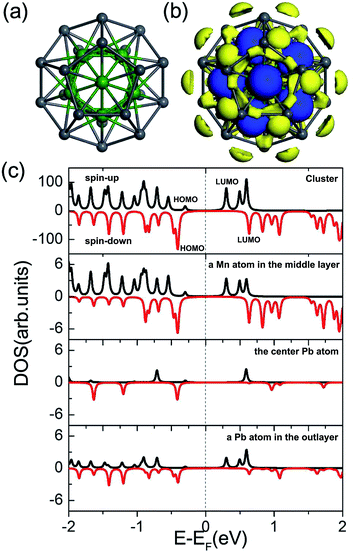 | ||
| Fig. 1 (a) The optimized structure of Pb@Mn12@Pb20 cluster, (b) its spin density distribution. (c) DOS of the Pb@Mn12@Pb20 cluster. | ||
To clearly illustrate the origin of the predicted MMs, we calculate the total density of states (DOS) of Pb@Mn12@Pb20 cluster, the partial DOS of one Mn atom in the middle layer, the center Pb atom and one Pb in the outlayer, and plot them in Fig. 1(c). Clearly, all calculated DOS are obviously spin-polarized. The spin-up states are filled more than the spin-down states for Pb@Mn12@Pb20 cluster and for the Mn atom, while this observation reverses for two Pb atoms, which are consistent with the predicted MMs. Note that, the positions of the highest occupied molecular orbital (HOMO) and the lowest unoccupied molecular orbital (LUMO) of Pb@Mn12@Pb20 cluster for the spin-up and spin-down electrons are remarkably different. The HOMO (LUMO) of the spin-up electrons locates at about −0.35 (0.3), while they locate at −0.4 (0.65) for the spin-down electrons. Then, the gaps between the HOMO and LUMO for two spin channels are also different, which are predicted to be 0.65 and 1.05 eV, respectively, although they are always underestimated at the GGA level. This predicted large MM and the remarkable difference in the electronic structures of the spin-up and spin-down states indicate that Pb@Mn12@Pb20 cluster is a possible candidate for designing molecular devices.
3.2 Pb@Mn12@Pb20 cluster on substrate
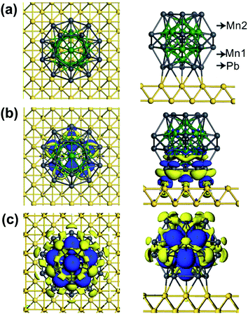
Before exploring the spin-polarized transport, we firstly examine the substrate effect on the geometric and magnetic properties of Pb@Mn12@Pb20 cluster. Here, Au(100) surface is taken as an example, which is simulated by a (6 × 6) supercell cell with periodic boundary conditions. The lattice constant in Au(100) slab model is 4.08 Å, taken from experimental distance. The cluster adsorbing on the hollow, bridge, and atop sites are considered. We find that the molecule prefers to adsorb Au(100) surface at the bridge site via a five-membered Pb ring, as shown in Fig. 2(a). The averaged vertical distance between Au(100) surface and the bottom five-member ring of Pb@Mn12@Pb20 cluster is about 2.65 Å, while the average Pb–Au bond length is 3.00 Å. This relatively small separation implies that the cluster–Au interaction is rather strong, which results in charge transfer between the cluster and Au surface. Fig. 2(b) plots the electron density difference, in which the blue and yellow regions represent charge accumulation and depletion, respectively. It is clear that the charge mainly transfers from the bottom part of Pb@Mn12@Pb20 cluster to these Au atoms locating around the anchoring interface. This observation is verified by the Mulliken charge analysis, and the net charge on the adsorbed Pb@Mn12@Pb20 cluster on Au(100) surface is predicted to be about +1.41|e| (here e is the electron charge).The MM of the Pb@Mn12@Pb20 cluster on Au(100) surface is predicted to be 30.3 μB, while the atomic MM of the labeled Mn1, Mn2, and Pb atoms in Fig. 2(a) is about 3.0, 2.8, and −0.2 μB, respectively. These results mean that the cluster magnetism is slightly enhanced due to the presence of Au(100) surface. This observation is totally distinct from a CoPc molecule adsorption on Au(111) surface, in which the molecular magnetism is quenched due to the molecule–substrate interaction.35 To understand this result, Fig. 2(c) shows the calculated spin density. Clearly, the spin density still mainly localizes around twelve Mn atoms, which still anti-ferromagnetically couple with these Pb atoms. The main reason for the enhanced cluster magnetism is that from these Pb atomic MMs at the bottom five-member are almost quenched due to the observed interfacial charge transfer, as shown in Fig. 2(b).
Fig. 3 plots the calculated total DOS of the Pb@Mn12@Pb20 cluster on Au(100) surface and the corresponding partial DOS of the Pb, Mn1 and Mn2 atoms, which are labeled in Fig. 2(a). Compared with the free Pb@Mn12@Pb20 cluster's results, the total DOS peaks are obviously broadened due to the rather strong cluster–substrate interaction. The partial DOS of the Pb atom in the bottom five-membered ring is virtually spin-restricted, which leads to the Pb atomic MM quenching.
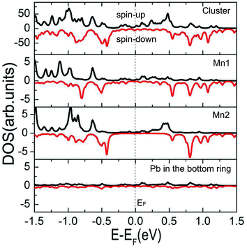 | ||
| Fig. 3 Total DOS of the Pb@Mn12@Pb20 cluster on Au(100) surface and the partial DOS of one Pb, Mn1, and Mn2 atoms, which are labeled in Fig. 2(a). | ||
3.3 Spin-polarized transport properties
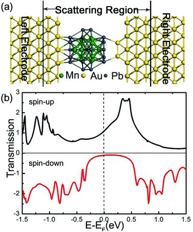
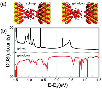
Now we turn to examine the spin-polarized transport properties of Pb@Mn12@Pb20 cluster. In a typical scanning tunneling microscopy experiment for single molecule transport measurements, a molecule always adsorbs on a flat surface (as one electrode), then a tip (act as the other electrode) is used to measure the current through the molecule. To mimic this situation, the Pb@Mn12@Pb20 cluster is sandwiched between two Au(100) electrodes. Fig. 4(a) illustrates the proposed junction, in which the left and right Au electrodes are modeled with two (5 × 5) supercells. This two-probe system can be divided into three parts: the left and right electrodes, and the central scattering region which includes Pb@Mn12@Pb20 cluster, two surface layers of the left electrode, and two Au adatoms (acting as a tip) on three surface layers of the right electrode. The Au–Pb anchoring distance is optimized to be about 2.65 Å, which indicates that the cluster is strongly coupled with electrode surfaces. The spin-resolved transmission spectra versus E − EF under zero-bias voltage of the junction is illustrated in Fig. 4(b). Here, the vertical black dotted line represents the position of the Fermi level, which is already set to zero for clarity, while the black and red solid lines stand for the transmission curves of the spin-up and spin-down electrons, respectively. It is clear that the conductance behavior of two spin channels is remarkably different. For instance, there is a broad and significant transmission peak locating around 0.4 V for the spin-up electrons, while for the spin-down electrons, the transmission coefficients within the energy range from −0.2 to 0.3 eV are small. The conductance of the spin-up electrons at the Fermi level is predicted to be 1.33G0 (G0 denotes the quantum constant, and equals to e2/h), which is significantly larger than that of the spin-down electrons (0.16G0). That to say, the spin-resolved transmission spectra of Pb@Mn12@Pb20 molecular junction exhibit robust transport spin polarization characteristics. To quantify this remarkable difference for the spin-up and spin-down electrons, we defined spin filter efficiency (SFE) as: SFE = (T↑ − T↓)/T↑. Here, T↑(EF) and T↓(EF) stand for the transmission coefficients of spin-up and spin-down electrons at the Fermi level, respectively. The SFE is predicted to be about 88.0%. Clearly, the conductance behavior through Pb@Mn12@Pb20 molecular junction is mainly governed by the spin-up electrons under the small bias voltage. This observation is similar to the results of europium-cyclooctatetraene,36 FeN4 complexes,37–39 and Mn@Au6 (ref. 28) cluster in our previous investigations.This observed spin filtering effect can be easily understood by exploring the local density of states (LDOS) of the Pb@Mn12@Pb20 molecular junction around the Fermi level. The spatial distribution of the LDOS at the Fermi level is plotted in Fig. 5(a), and the calculated DOS of the scattering region is presented in Fig. 5(b), respectively. It is clear that the LDOS of the spin-up electrons delocalized over around the whole molecule junction, which provides a good transport channel. On the contrary, as for the spin-down electrons, the LDOS mainly localize at the right region of the cluster, and resulting in a small conductance at the Fermi level. Actually, the positions of these DOS peaks correspond well with the transmission peaks. The LUMO of the spin-up channel is localized, which does not contribute an obvious transmission peak. The transmission peak at 0.4 V is contributed by the perturbed LUMO+1 and LUMO+2.
The spin-polarized current–voltage (I–V) curves through Pb@Mn12@Pb20 molecular junction are calculated and plotted in Fig. 4. In our calculations, at each bias voltage, the current is determined self-consistently Landauer–Buttiker formula under the non-equilibrium condition, black and red lines stand for spin-up and spin-down electrons, respectively. Clearly, the current of the spin-up electrons is significant larger than that of the spin-down ones. To quantify the current difference between the spin-up and spin-down electrons, the ratio of currents is defined as R(V) = |I↑/I↓|. The predicted R is up to 14 within the examined bias voltage range, which is readily measurable in experiments. In other words, the I–V results through Pb@Mn12@Pb20 molecular junction confirm this proposed spin-filtering device can works at finite bias voltage (Fig. 6).
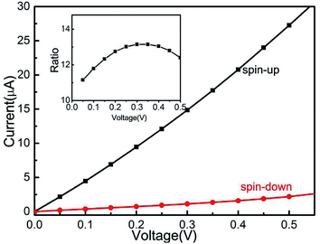 | ||
| Fig. 6 Calculated spin-resolved I–V curves of the Pb@Mn12@Pb20 molecular junction. Here, the inset denotes the rectification ratio versus bias voltage. | ||
In general, the distance between the molecule and the electrode is variable in experiments.40 We examine the dependence of transport properties of the Pb@Mn12@Pb20 junction on the different Au–Pb anchoring distances. Even the end Au–Pb distance is elongated to be 3.0 Å, the main features of the spin-resolved transmission curves through the junction do not significantly change. The T↑ and T↓ are predicted to be 1.08 and 0.10G0, and the corresponding SFE is about 90.7%. That is to say, the transport spin polarization characteristics is not sensitive to the end Au–Pb anchoring distance.
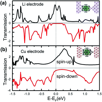
Note that the exact anchoring configuration of molecular devices in experiments is a ‘blackbox’ so far.41–45 Here, we propose two Pb@Mn12@Pb20-based junctions with different anchoring configurations between Li and Cu(100) electrodes to examine whether the spin filtering effect exists or not. Three Li atoms and on Cu atom are pulled outwards the surfaces for the Li and Cu electrodes to simulate the different anchoring configurations, as schematically illustrated with inserts in Fig. 7(a) and (b), and the corresponding zero-bias energy dependent spin-resolved transmission spectra of the Pb@Mn12@Pb20 cluster connected to Li and Cu electrodes are plotted, respectively. It is clear that the transport spin polarization characteristics are still robust. For example, around the Fermi level, there is a significant and broad transmission peak for the spin-up electrons, and the T↑ is 1.75G0 for the Li electrodes, while for the spin-down electrons, their transmission coefficients are small, and the corresponding T↓ is about 0.03G0. The SFE for junction with Li and Cu electrodes is predicted to be about 98.3% and 76.1%, respectively. As for the same electrodes, such as Au and Li as examples, we also observe the obvious transport spin polarization feature in the zero-bias energy dependent spin-resolved transmission spectra (see ESI†). That is to say, the predicted spin-filtering effect is not sensitive to the detailed anchoring configurations and the adopted electrode materials. This observation highlights this kind of magnetic three-shell icosahedral matryoshka cluster with huge MM for promising applications in molecular spintronic devices.
4 Conclusions
Based on DFT calculations combined with the NEGF technique, the electronic structures, magnetic and spin transport properties of the Pb@Mn12@Pb20 cluster are explored. Theoretical results indicate that the Pb@Mn12@Pb20 cluster has a huge magnetic moment of 28.0 μB, mainly contributed twelve Mn atoms in the middle layer, which anti-ferromagnetically couple to the central Pb atom and the Pb atoms in the outlayer. The zero-bias transmission coefficients of the spin-up electrons through Pb@Mn12@Pb20 cluster sandwiched between two Au(100) electrodes are significantly larger than that of the spin-down electrons. The spin filter efficiency is predicted to be 83.2%. Moreover, the proposed model device can stably work at finite bias voltage, and this observed spin filtering effect is not sensitive to the anchoring distance and the adopted electrode materials. These findings indicate that this kind of magnetic three-shell icosahedral matryoshka cluster with huge MM can be used to design spin-filtering device.Acknowledgements
This work was partially supported by the National Key Basic Research Program (No. 2014CB921101), by the State Key RD Fund of China (No. 2016YFA0200604), by the National Natural Science Foundation of China (No. 21473168 and 11634011), by the Innovative Program of Development Foundation of Hefei Center for Physical Science and Technology (Q. L.). J. H. thanks the Natural Science Foundation of the Anhui Higher Education Institutions (No. KJ2016A144) and the Natural Science Foundation of Anhui Province (No. 1408085QB26). Computational resources have been provided by CAS, Shanghai and USTC Supercomputer Centers.References
- A. Aviram and M. A. Ratner, Chem. Phys. Lett., 1974, 29, 277 CrossRef CAS.
- M. Kiguchi and S. Kaneko, ChemPhysChem, 2012, 13, 1116 CrossRef CAS PubMed.
- C. C. Jia, A. Migliore, N. Xin, S. Y. Huang, J. Y. Wang, Q. Yang, S. P. Wang, H. L. Chen, D. M. Wang, B. Y. Feng, Z. R. Liu, G. Y. Zhang, D. H. Qu, H. Tian, M. A. Ratner, H. Q. Xu, A. Nitzan and X. F. Guo, Science, 2016, 352, 1443–1445 CrossRef CAS PubMed.
- C. D. Frisbie, Science, 2016, 352, 1394–1395 CrossRef CAS PubMed.
- C. Joachim, J. K. Gimzewski and A. Aviram, Nature, 2000, 408, 541 CrossRef CAS PubMed.
- J. Chen, M. A. Reed, A. M. Rawlett and J. M. Tour, Science, 1999, 286, 1550 CrossRef CAS PubMed.
- M. Galperin, M. A. Ratner and A. Nitzan, Nano Lett., 2005, 5, 125 CrossRef CAS PubMed.
- S. Yasuda, T. Nakamura, M. Matsumoto and H. Shigekawa, J. Am. Chem. Soc., 2003, 125, 16430 CrossRef CAS PubMed.
- S. Yeganeh, M. Galperin and M. A. Ratner, J. Am. Chem. Soc., 2007, 129, 13313 CrossRef CAS PubMed.
- E. Ruiz, Phys. Chem. Chem. Phys., 2014, 16, 14–22 RSC.
- H. Ren, G. P. Zhang, N. Lin, L. Deng, Y. Luo and F. Huang, Phys. Chem. Chem. Phys., 2016, 18, 26586–26594 RSC.
- L. Zhu, F. Zou, J. H. Gao, Y. S. Fu, G. Y. Gao, H. H. Fu, M. H. Wu, J. T. Lü and K. L. Yao, Nanotechnology, 2015, 26, 315201 CrossRef CAS PubMed.
- A. Nitzan and M. A. Ratner, Science, 2003, 300, 1384–1389 CrossRef CAS PubMed.
- C. C. Kaun and T. Seideman, Phys. Rev. B: Condens. Matter Mater. Phys., 2008, 77, 033414 CrossRef.
- I. Aviv-Harel and Z. Gross, Coord. Chem. Rev., 2011, 255, 717–736 CrossRef CAS.
- H. Palmer, in Molecular electronic structures of transition metal complexes I, Springer, 2011, pp. 49–89 Search PubMed.
- X. X. Zhang, Y. Wang, H. P. Wang, L. Alane, G. Gantefoer, K. H. Bowen, J. U. Reveles and S. N. Khanna, J. Am. Chem. Soc., 2013, 135, 4856–4861 CrossRef CAS PubMed.
- K. Damianos, P. Solokha and R. Ferrando, RSC Adv., 2013, 3, 9419–9430 RSC.
- S. Stegmaier and T. F. Fässler, Angew. Chem., Int. Ed., 2012, 51, 2647–2650 CrossRef CAS PubMed.
- K. Xu, J. Huang, Z. Y. Guan, Q. X. Li and J. L. Yang, Chem. Phys. Lett., 2012, 535, 111–115 CrossRef CAS.
- F. K. Sheong, W. J. Chen, H. Kim and Z. Y. Lin, Dalton Trans., 2015, 44, 7251–7257 RSC.
- J. Huang, R. Xie, W. Y. Wang, Q. X. Li and J. L. Yang, Nanoscale, 2016, 8, 609–616 RSC.
- L. H. Yu and D. Natelson, Nano Lett., 2004, 4, 79 CrossRef CAS.
- A. Saffarzadeh, J. Appl. Phys., 2008, 103, 083705 CrossRef.
- T. Xu, J. Huang and Q. X. Li, Chin. J. Chem. Phys., 2014, 27, 668–673 Search PubMed.
- J. L. Wang, J. Bai, J. Jellinek and X. C. Zeng, J. Am. Chem. Soc., 2007, 129, 4110 CrossRef CAS PubMed.
- S. Stegmaier and T. F. Fässler, J. Am. Chem. Soc., 2011, 133, 19758 CrossRef CAS PubMed.
- J. Huang, W. Y. Wang, S. F. Yang, Q. X. Li and J. L. Yang, Chem. Phys. Lett., 2013, 590, 111–115 CrossRef CAS.
- X. M. Huang, J. J. Zhao, Y. Su, Z. F. Chen and R. B. King, Sci. Rep., 2014, 4, 6915 CrossRef CAS PubMed.
- M. J. Moses, J. C. Fettinger and B. W. Eichhorn, Science, 2003, 300, 778 CrossRef CAS PubMed.
- J. M. Soler, E. Artacho, J. D. Gale, A. García, J. Junquera, P. Ordejón and D. Sánchez-Portal, J. Phys.: Condens. Matter, 2002, 14, 2745–2779 CrossRef CAS.
- J. Taylor, H. Guo and J. Wang, Phys. Rev. B: Condens. Matter Mater. Phys., 2001, 63, 245407 CrossRef.
- M. Brandbyge, J.-L. Mozos, P. Ordejón, J. Taylor and K. Stokbro, Phys. Rev. B: Condens. Matter Mater. Phys., 2002, 65, 165401 CrossRef.
- J. P. Perdew and Y. Wang, Phys. Rev. B: Condens. Matter Mater. Phys., 1992, 45, 13244 CrossRef.
- A. D. Zhao, Q. X. Li, L. Chen, H. J. Xiang, W. H. Wang, S. Pan, B. Wang, X. D. Xiao, J. L. Yang, J. G. Hou and Q. S. Zhu, Science, 2005, 309, 1542 CrossRef CAS PubMed.
- K. Xu, J. Huang, S. L. Lei, H. B. Su, F. Y. C. Boey, Q. X. Li and J. L. Yang, J. Chem. Phys., 2009, 131, 104704 CrossRef.
- J. Huang, W. Y. Wang, S. F. Yang, Q. X. Li and J. L. Yang, Nanotechnology, 2012, 23, 255202 CrossRef PubMed.
- T. Miyamachi, M. Gruber, V. Davesne, M. Bowen, S. Boukari, L. Joly, F. Scheurer, G. Rogez, T. K. Yamada, P. Ohresser, E. Beaurepaire and W. Wulfhekel, Nat. Commun., 2012, 3, 938 CrossRef PubMed.
- J. Huang, W. Y. Wang, S. F. Yang, H. B. Su, Q. X. Li and J. L. Yang, Chem. Phys. Lett., 2012, 539, 102–106 CrossRef.
- B. Q. Xu and N. J. Tao, Science, 2003, 301, 1221 CrossRef CAS PubMed.
- A. N. Pasupathy, R. C. Bialczak, J. Martinek, J. E. Grose, L. A. K. Donev, P. McEuen and D. Ralph, Science, 2004, 306, 86–89 CrossRef CAS PubMed.
- T. Ono and K. Hirose, Phys. Rev. Lett., 2007, 98, 026804 CrossRef PubMed.
- A. N. Pasupathy, J. Park, C. Chang, A. V. Soldatov, S. Lebedkin, R. C. Bialczak, J. E. Grose, L. Donev, J. P. Sethna, D. C. Ralph and P. L. McEuen, Nano Lett., 2005, 5, 203–207 CrossRef CAS PubMed.
- Y. Yasutake, Z. J. Shi, T. Okazaki, H. Shinohara and Y. Majima, Nano Lett., 2005, 5, 1057–1060 CrossRef CAS PubMed.
- C. M. Guédon, H. Valkenier, T. Markussen, K. S. Thygesen, J. C. Hummelen and S. J. van der Molen, Nat. Nanotechnol., 2012, 7, 305–309 CrossRef PubMed.
Footnote |
| † Electronic supplementary information (ESI) available: The structural models for the free cluster, the cluster adsorption on Au(100) surface at the bridge site, and the cluster is sandwiched between Au electrodes. See DOI: 10.1039/c7ra01003f |
| This journal is © The Royal Society of Chemistry 2017 |

