 Open Access Article
Enhanced temperature stability and exceptionally high electrical contrast of selenium substituted Ge2Sb2Te5 phase change materials†
Christine Kocha,
Anna-Lena Hansena,
Torben Dankwortb,
Gerrit Schienkea,
Melf Paulsena,
Dominik Meyerc,
Martin Wimmerc,
Matthias Wuttigc,
Lorenz Kienleb and
Wolfgang Bensch *a
*a
aInstitute for Inorganic Chemistry, University of Kiel, Max-Eyth-Str. 2, 24118 Kiel, Germany. E-mail: wbensch@ac.uni-kiel.de
bInstitute for Materials Science, University of Kiel, Kaiserstr. 2, 24143 Kiel, Germany
cInstitute of Physics, RWTH Aachen University, Sommerfeldstr. 14, 52056 Aachen, Germany
First published on 20th March 2017
Abstract
Ge2Sb2Te4Se (I) and Ge2Sb2Te2Se3 (II) thin films were synthesized and compared to the pure telluride Ge2Sb2Te5. In situ X-ray diffraction (XRD) and in situ transmission electron microscopy (TEM) investigations revealed a remarkably increased stability of the as-deposited amorphous phase. The transition temperature (beginning transition) determined with in situ XRD increases from 135 °C for the pure telluride to 165 °C for (I) and to 225 °C for (II). An identical trend for the transition temperatures (transition complete) was observed by sheet resistance measurements with values of 153, 190 and 243 °C, respectively. Optical properties determined with Fourier-transform-infrared (FTIR) spectroscopy and variable incident angle spectroscopic ellipsometry (VASE) exhibit a significant energy-dependent behavior of the dielectric functions. Major changes of the maxima and intensities of the extinction coefficients and the indices of refraction are observed with increasing Se content. These results are in agreement with the results obtained by Rietveld refinement and TEM. The incorporation of Se into the structure of the metastable cubic phase causes small distortions, leading to a phase transition. Electrical sheet resistance measurements reveal an exceptionally large electrical contrast between the amorphous and crystalline phases, which is increased by a factor of 100 for compound (II) compared to established phase change materials.
Introduction
Today, data storage is of particular technological importance. For the last few thousands of years information was stored, starting with drawings and paintings, improving with letters and books, up to computers containing data storage devices. Because of the increasing amount of data, larger and faster memory devices of smaller sizes are required. In case of optical data storage, long-term stability, repeatability and reliability need to be improved, as well as the data density and the opto-electronic contrast. Additionally, the costs of the materials should be as low as possible and easy fabrication is required.1,2 These criteria are met for phase change materials (PCM).3,4 Most phase change materials are based on the pseudo-binary section of the binary compounds GeTe and Sb2Te3 yielding compositions like (GeTe)m(Sb2Te3)n. Another very interesting composition is AIST, a combination of the elements Ag, In, Sb and Te.5 These materials can rapidly and reversibly be switched between an amorphous and a crystalline state applying a laser with short pulses and high powers. The amorphous and crystalline states have remarkably different optical properties that are easily detected by the laser. For erasing the bit (recrystallization) a longer lasting pulse with lower intensity is used.During the last decades three different generations of optical data storage devices were developed: compact discs (CD, using a laser wavelength of 830 nm), digital versatile discs (DVDs, 650 nm) and Blu-ray™ discs (BD, 405 nm). Further decreasing the laser wavelength has been proven difficult due to several challenges including the lack of suitable laser diodes, but also a decreasing contrast of phase change materials at shorter wavelengths. Further, phase change materials have been studied for their application potential in non-volatile electronic memories. They can be rapidly and reversibly switched if a low voltage pulse is applied and they have already proven excellent scaling potential. Yet, there are still a number of issues to be addressed in order to understand the full potential of these novel memories. Two questions are of particular interest for applications at elevated temperatures, such as automotive applications, namely: at which temperature will the amorphous phase crystallize and how high is the resistance of the amorphous phase. While the stability of the amorphous phase is crucial for applications at elevated temperatures, a high resistance of the amorphous state could facilitate realizing a multi-level memory.6,7
In recent years, two major research approaches were followed for further improvement of phase change materials. One research direction is focused on unravelling the atomistic origin of the high switching speeds, the aging of the amorphous state and the pronounced property contrast between the two states.8 The structure of the crystalline phase is in most cases a distorted rock salt structure with different vacancy concentrations in the cation sublattice depending on the chemical composition.9–12 From a chemical point of view it is not easy to explain that Ge and Sb in Ge2Sb2Te5 each are in an octahedral environment of Te2− anions. One approach to rationalize this bonding situation is called resonant bonding where sharing of electrons (covalent bonds) leads to stabilization of highly symmetric coordination. To avoid confusion with the term resonant bonding used in organic chemistry to describe the bonding situation in high symmetric materials like benzene or graphite, resonant bonding in PCMs has a different meaning.6,13–15
The local atomic structures of the different phases were also intensively investigated.16–22 Despite many efforts, the short-range coordination of the different atoms in the amorphous structure are still under debate in literature.16,23–26 These problems demonstrate that it is not trivial to investigate and understand the reactions on atomic scale of the phase change, yet being the essential issue for designing new materials. Hence, in a second approach, scientists have tried to identify new compounds, which also exhibit the characteristic properties of phase change materials.
So far, many studies have focused on Ge2Sb2Te5.27–30 Due to its excellent properties it was used as the DVD-RW material. Other well investigated compounds are GeCu2Te3 (ref. 31–33) and Ge8Sb2Te11 being the active material in BD-RW discs or binaries such as Ge15Sb85,34 GeTe35 and GaSb,36–39 respectively. Several studies deal with the substitution or doping of established phase change materials.40–45 Samples with compositions (Ge2Sb2Te5)1−xSex (x = 0–0.5) were recently investigated, showing a significantly different crystallization behavior. For x ≥ 0.1 the stable hexagonal structure is directly formed at T ≥ 150 °C, while the metastable cubic phase could only be observed for x ≤ 0.02. With increasing Se content the optical band gap becomes larger. In addition, the resistance, threshold voltage and thermal stability increased with x. For the Se substituted materials a relatively low crystallinity of the crystalline phases was observed.46,47 Compared to Ge2Sb2Te5 no significant improvement in properties could be observed and a relationship of properties with structural changes could not be established.
In our ongoing work the impact of the substitution of Te in Ge2Sb2Te5 by Se on the material properties was investigated. The substitution in the anion substructure of the metastable cubic rock salt structure should lead to local distortions, a decreased metallic character and a larger electronegativity difference, which increases at the same time hybridization and ionicity. As a result of these pronounced changes of the physico-chemical properties significant alterations of the optical and electrical behavior are expected. Additionally, the bond strength and therefore the phase change transition temperatures should be altered. The final goal of the present investigation is to establish a relationship between the change in the chemical bonding by chemical substitution of Te by Se and the resulting properties. The results of these experiments and the observed trends concerning the opto-electronic properties and the bonding characteristics are reported.
Experimental section
Thin film samples of Ge2Sb2Te5 and Ge2Sb2Te4Se (I) were prepared by DC magnetron sputtering using stoichiometric targets (Umicore, 99.99%) bonded to water cooled copper plates. The base pressure in the sputter chamber was <2 × 10⁻⁶ mbar, the argon current was fixed at 20 sccm for all deposition runs. Ge2Sb2Te5 was deposited by using a single target of 10 cm diameter at 20 W. (I) was prepared via co-sputtering of GeSb2Te4 (5 cm diameter) at 30 W and GeSe (10 cm diameter) at 25 W.All substrates had a size of 2 × 2 cm. Thin film samples of ∼700 nm thickness were prepared on (1 0 0) silicon single crystal substrates, glass substrates, glass substrates with previously sputtered chromium contacts in the corners (for electrical measurements) and silicon substrates coated with ∼200 nm aluminum layers (for optical measurements). Thin samples of ∼35 nm were deposited on nickel TEM-grids, coated with a thin amorphous carbon layer. The deposition times of the thick and thin films were 3688 s (∼700 nm) and 132 s (∼35 nm) for Ge2Sb2Te5 and 2000 s (∼700 nm) and 75 s (∼35 nm) for Ge2Sb2Te4Se (I).
Ge2Sb2Te2Se3 (II) was prepared by thermal co-evaporation of single elements in an ultra-high vacuum chamber (Omicron NanoTechnology), using single element Knudsen cells containing the utilized elements (Chempur 99.999%) at different temperatures, listed in Table 1. The base pressure in the chamber was p < 1 × 10⁻⁸ mbar. A beam flux monitor was used to ensure stable evaporation rates.
| Element | Germanium | Antimony | Tellurium | Selenium |
| Temperature/°C | 1100 | 348 | 233 | 140 |
| Deposition time | 9 h (700 nm); 30 min (∼35 nm) | |||
It should be noted that it is very important to find a reliable method to determine the compositions, because the signals of the elements partly overlap in most common analytic techniques due to their similar electronic structure. We found that electron probe micro-analysis (EPMA) is the most promising and precise method for investigating the X-ray emission L-series of the elements, using an acceleration voltage of 10, 16 and 22 kV. The EPMA measurements were taken with a Cameca SX 100, yielding composition values close to the required stoichiometries. A Bruker DektaktXT profilometer was used to determine the film thicknesses.
X-Ray diffraction (XRD) was performed in θ–θ geometry using an X'Pert Pro MPD diffractometer (PANalytical; Cu Kα1,2 radiation), equipped with a Göbel mirror and a PIXcel detector. Temperature dependent in situ diffraction was performed in an Anton Paar HTK 1200N high temperature chamber in helium (99.999%) atmosphere to prevent oxidation of the samples. The temperature was increased stepwise with a heating rate of 5 K min−1 from 28 °C up to 360 °C. The patterns were collected within one hour over a range of 15–65° 2θ at constant temperature. The scans for the Rietveld refinements were performed on a flat stage using the same setup in a range of 10–100° 2θ (step size 0.05°).
Rietveld refinements were carried out using the Program TOPAS Academic (Version 6).48 In order to calculate crystallite sizes the fundamental parameter approach was employed.49,50 To refine the anisotropic peak broadening caused by strain we used a spherical harmonics to calculate the Lorentz width as a function of tan(θ). To correct texture effects, which are typical for thin film analysis, a spherical harmonics was employed.
In situ heating TEM experiments were performed by a FEI Tecnai F30 G2 using a GATAN double tilt heating holder 652. The heating rate was set to 10 K min−1. After the desired temperature was reached, a holding time was utilized until minimum sample drift and temperature equilibrium were achieved. Subsequently electron diffraction patterns were recorded at the rim of the grid, close to the measuring and heating device to ensure high accuracy of the actual temperature of the sample. For HRTEM and bright field imaging the heating was interrupted to ensure no sample drift.
To investigate the optical properties FTIR and ellipsometry measurements were done. FTIR spectra have been collected using a Bruker IFS 66ν/s with a resolution of 0.12 meV. To exclude drift effects the samples and a gold reference were measured alternately. The measured spectra were renormalized by a gold reference to obtain the final spectrum. For ellipsometry measurements a J. A. Woollam M-2000UI equipped with deuterium and halogen lamps as light sources was used. The incidence angles were 65°, 70° and 75°. The examined energy ranges were 0.05–1 eV for FTIR and 0.7–5.2 eV for ellipsometry. All measurements were performed with the as-deposited amorphous samples as well as the metastable crystalline samples each on aluminum coated silicon substrates at room temperature. These substrates were prepared by sputter deposition of an aluminum target with the same process as described above. The values for the dielectric constants as well as the index of refraction n and the extinction coefficient k were obtained by fitting the spectra using SCOUT software.51 Therefore the same assumptions as in ref. 42 were made.
Sheet resistance measurements were performed using a four-point-probe setup according to van-der-Pauw52–55 with argon (99.996%) as protective gas. ∼700 nm thick samples on glass substrates with chromium contacts in each corner were heated with a heating rate of 5 K min−1 up to 360 °C. This temperature was held constant for 30 min and then the samples were cooled down to room temperature. Because of the large density change of up to 10% between the amorphous and crystalline phases which unfortunately cannot be investigated and corrected during the resistivity measurements the resistance of the films instead of the resistivity was investigated.
Results and discussion
Structural characterization by in situ XRD and TEM heating experiments
In situ X-ray diffraction and TEM investigations were performed to independently investigate the structure and crystallization of the films. Both methods confirm that all as deposited films are amorphous. Thin films of Ge2Sb2Te5 crystallize in the metastable cubic (Fm![[3 with combining macron]](https://www.rsc.org/images/entities/char_0033_0304.gif) m) and the stable primitive trigonal (P
m) and the stable primitive trigonal (P![[3 with combining macron]](https://www.rsc.org/images/entities/char_0033_0304.gif) m1) phase, respectively.56
m1) phase, respectively.56
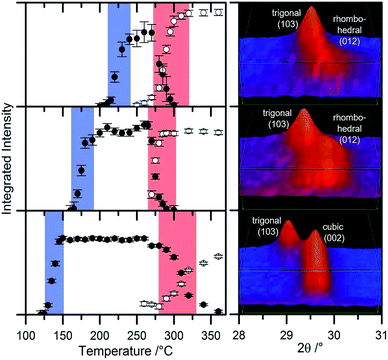
For the accurate determination of the transition temperatures the intensities of the (002) reflection of the cubic and the (103) reflection of the primitive trigonal phase were analyzed as function of temperature (Fig. 1 and 2). While the 1st transition temperature increases with higher selenium content the temperature of the 2nd transition to the thermodynamically stable phase remains quite constant at around 270–290 °C. All three samples are stable until 360 °C.
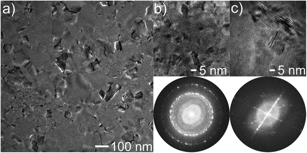
In situ TEM heating experiments were performed by monitoring the formation of diffraction spots in the Selected Area Electron Diffraction (SAED) pattern. A representative temperature resolved image of this process is depicted in Fig. 3 for Ge2Sb2Te2Se3. Crystallization started at 132 °C, 160 °C and 222 °C, for Ge2Sb2Te5, Ge2Sb2Te4Se and Ge2Sb2Te2Se3, respectively (for details see Fig. S1 and S2†). Further, diffuse streaks in the ED pattern were found for Ge2Sb2Te2Se3 after reaching the temperature of 250 °C (Fig. 3). These diffuse streaks indicate the formation of planar defects which can be attributed to vacancy layers forming along the (111) planes with respect to the cubic symmetry.9,57,58
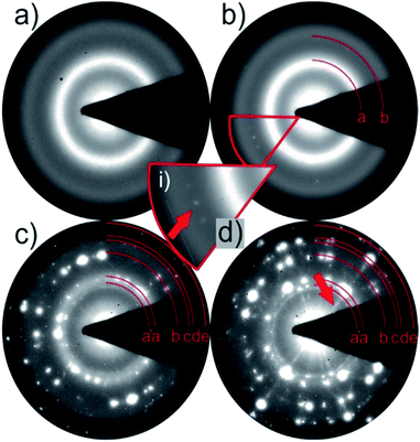 | ||
| Fig. 3 SAED pattern of Ge2Sb2Te2Se3 (a) at room temperature; (b) crystallization starts at 222 °C (diffraction spots marked with red arrow); (c) growth of larger grains at 240 °C; (d) C diffuse streaks along [111] (rhombohedral cell) indicate formation of vacancy layers at 250°. Measured d-values fit to the calculated data can be found in Table S3.† | ||
A comparison of the transformation temperatures determined by in situ XRD and in situ TEM are displayed in Table 2. Phase change temperatures exhibit convincing agreement and confirm the monotonous increase of the crystallization temperature with increasing Se content. The values of Ge2Sb2Te5 correspond well to those reported in literature.27,59,60 Further, the substitution of Te by Se leads to a significant stabilization of the amorphous phase and therefore to a stabilization of amorphous areas/bits in data storage applications. Similar effects were also observed for other Ge–Sb–Te phases upon Se substitution.40
| Temperatures determined for | Via in situ XRD measurements | Via in situ TEM measurements | |
|---|---|---|---|
| 1 | 2 | 1 | |
| Ge2Sb2Te5 | 130 °C | 290 °C | 132 °C |
| Ge2Sb2Te4Se (I) | 165 °C | 270 °C | 160 °C |
| Ge2Sb2Te2Se3 (II) | 220 °C | 280 °C | 222 °C |
Bright field (BF) and high resolution TEM (HRTEM) images of Ge2Sb2Te5 after the heating process revealed a mixture of larger grains with 100 nm size and nanocrystals marked by red and blue arrows in Fig. 4a, respectively. In comparison Se substituted films showed significantly smaller crystallites, cf. Fig. 4b and c displaying exclusively nanosized crystallites for (I) and (II).
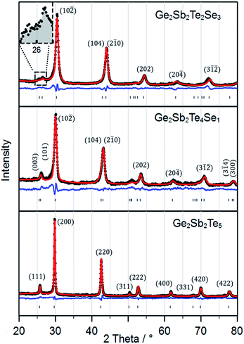
Room temperature XRD data was analyzed via Rietveld refinement of the metastable phase revealing the same tendency for the crystallite size as found in TEM measurements (see Table 3 and Fig. 5).
![[3 with combining macron]](https://www.rsc.org/images/entities/char_0033_0304.gif) m) are given according to the hexagonal setting of the space group. Further information is given in Table S4
m) are given according to the hexagonal setting of the space group. Further information is given in Table S4
| Chemical formula | 225 | * | I | II | |
| Space group | Fm![[3 with combining macron]](https://www.rsc.org/images/entities/char_0033_0304.gif) m (225) m (225) |
R![[3 with combining macron]](https://www.rsc.org/images/entities/char_0033_0304.gif) m (166) m (166) |
R![[3 with combining macron]](https://www.rsc.org/images/entities/char_0033_0304.gif) m (166) m (166) |
R![[3 with combining macron]](https://www.rsc.org/images/entities/char_0033_0304.gif) m (166) m (166) |
|
| Cell parameter (Å) | a | 6.0251 | 4.2624 | 4.1976 | 4.125 |
| c | — | 10.4408 | 10.4456 | 10.4364 | |
| c/a | 2.4495 | 2.4885 (+0.0390) | 2.5300 (+0.0805) | ||
| Crystallite size (nm) | 52 | — | 18 | 25 | |
| RBragg | 1.78 | — | 1.01 | 1.92 | |
The refinement indicated a symmetry reduction due to the incorporation of Se and a resulting distortion of the lattice along [111]. The latter caused a shift of the (220) reflection and anisotropic strain broadening. In the diffraction pattern of Ge2Sb2Te2Se3 we finally observe a splitting of the cubic (111) reflection, typically for a reduced symmetry (inset of Fig. 5).
To account for the lower symmetry, the cubic cell was transformed into the trigonal subgroup R![[3 with combining macron]](https://www.rsc.org/images/entities/char_0033_0304.gif) m (hexagonal axes). Due to the small crystallite size and the additional strain broadening, a splitting of the (220) reflection could not be observed, but its shift to lower scattering angle clearly represents a reduction of cubic symmetry even if the distortion itself is small. When compared to the transformed undistorted cell, it is apparent that the deviation from the cubic aristotype is more pronounced for the higher Se content. Calculated d-values based on the Rietveld refinements match closely with measured d-values of ED patterns (Tables S1–S3†).
m (hexagonal axes). Due to the small crystallite size and the additional strain broadening, a splitting of the (220) reflection could not be observed, but its shift to lower scattering angle clearly represents a reduction of cubic symmetry even if the distortion itself is small. When compared to the transformed undistorted cell, it is apparent that the deviation from the cubic aristotype is more pronounced for the higher Se content. Calculated d-values based on the Rietveld refinements match closely with measured d-values of ED patterns (Tables S1–S3†).
Optical properties
It was already pointed out that resonant bonding is an indispensable property for high optical contrast of PCMs. As a result of the distortion in the substituted samples the octahedral environment of the atoms is distorted which leads to a misalignment of the p-orbitals and therefore to a significant reduction of the resonant bonding in the metastable phase. This corresponds well with the so called “treasure map” for PCM (Fig. 6).14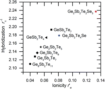 | ||
| Fig. 6 Calculated values of ionicity and degree of hybridization for some established phase change materials and the substituted compounds.14 Used radii according to ref. 61. | ||
All established PCMs for optical data storage devices are located in a well-defined area in the map. It seems that the limit of this area for successful optical data storage materials is reached by the values given by the hybridization of Ge2Sb2Te2Se3. This assumption is confirmed by investigations of the optical properties.
The dielectric function ε contains the two dielectric constants ε1 (real part) and ε2 (imaginary part).
| ε = ε1 + iε2 | (1) |
A conversion of the dielectric function leads to the index of refraction n (2) and the extinction coefficient k (3):
| ε1 = n2 − k2 | (2) |
| ε2 = 2nk | (3) |
Fig. 7 displays the real and the imaginary part of the dielectric functions of the materials. A significant decrease of the maximum intensity and a shift to higher energies depending on the selenium content is observed. This can be explained by the structural distortions leading to a decrease of resonant bonding, which reduces ε1 of the crystalline samples of (I) and (II) and explains the behavior.
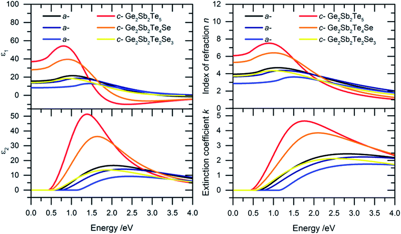 | ||
| Fig. 7 Left: Dielectric functions ε1 (top) and ε2 (bottom) of the amorphous (a-) and crystalline (c-) samples. ε1 becomes constant for energies below the optical band gap. Functions of ε2 are depicted without the Drude term. Functions of ε2 with the Drude term are seen in Fig. S3.† The crystalline samples were annealed at 160 °C (225), 210 °C (I) and 260 °C (II). Right: Index of refraction n (top) and extinction coefficients k (bottom) of the a- and c-samples. k turns out to be zero at energies below the band gaps. | ||
According to formula (1) and (2) the same trend of the energy dependence of n and k is observed (Fig. 7). For typical amorphous phase change materials the index of refraction is ∼50% larger in the crystalline state (e.g. Ge2Sb2Te5).15 The substitution of Te by Se leads to a drastic decrease of the difference between the amorphous and crystalline indices of refraction. It is remarkable that the optical constants of the crystalline Ge2Sb2Te2Se3 sample are below amorphous Ge2Sb2Te5. This observation implies that the ability of crystalline Ge2Sb2Te2Se3 to reflect light in the appropriate energy range is even worse compared to amorphous Ge2Sb2Te5.
Table 4 summarizes the values for the optical constant ε∞ and the optical bandgap Eg. The values of the amorphous and crystalline phases of Ge2Sb2Te5 correspond well with the values reported in literature.15,62,63
![[thin space (1/6-em)]](https://www.rsc.org/images/entities/char_2009.gif) 000 method which is exactly the energy where the absorption reaches 10
000 method which is exactly the energy where the absorption reaches 10![[thin space (1/6-em)]](https://www.rsc.org/images/entities/char_2009.gif) 000 cm−1 (ref. 62)
000 cm−1 (ref. 62)
| Optical constant ε∞ | Optical bandgap Eg | |||||
|---|---|---|---|---|---|---|
| a | c | %increase | a | c | %decrease | |
| 225 | 15.6 | 37.1 | 138 | 0.77 | 0.53 | 31 |
| I | 13.4 | 28.1 | 110 | 0.88 | 0.59 | 33 |
| II | 8.2 | 13.9 | 70 | 1.23 | 0.70 | 43 |
With increasing selenium content ε∞ decreases while Eg increases due to the reduced metallic behavior as a result of the substitution of Te by Se. Applying eqn (4) the contribution of resonance bonding can be estimated which is basically the value of the increase of ε∞ in %.15
| εcrystalline∞/εamorphous∞ − 1 | (4) |
The resonance bonding decreases with increasing Se content which can be explained (just like the extraordinary low optical constant of the crystalline phase of (II)) via the decrease of resonant bonding in the samples (I) and especially (II). The knowledge of all optical constants allows calculation of the absolute reflectivity of the amorphous and crystalline samples. Fig. 8 displays absolute reflectivity and total contrast calculated according to (5).42
 | (5) |
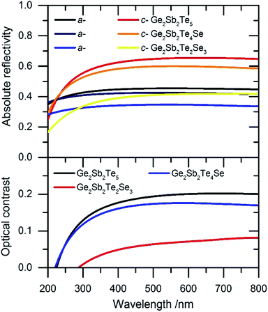 | ||
| Fig. 8 Calculated absolute reflectivity (top) of the amorphous and crystalline films and total contrast (bottom) of the materials. | ||
Due to the pronounced decrease of the absolute reflectivity of the substituted crystalline samples the optical contrast decreases from ∼20% for Ge2Sb2Te5 to ∼17% for (I) and ∼8% for (II).
Although a slight shift of the maxima of the dielectric constants to higher energies e.g. smaller wavelengths is observed, the Se substituted samples seem to be not suitable for optical phase change data storage. The optical properties confirm the assumption that the limit of the hybridization for materials used in optical data storage devices is reached by values around 2.24.
Sheet resistance measurements
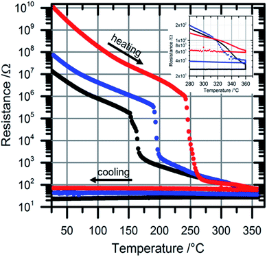
Temperature dependent sheet resistance measurements are shown in Fig. 9. It can be safely assumed that the influence of the slightly different film thicknesses onto resistance data is negligible. The sheet resistances for the amorphous films at room temperature are ∼13 MΩ for Ge2Sb2Te5, ∼73 MΩ for Ge2Sb2Te4Se and ∼11 GΩ for Ge2Sb2Te2Se3.In line with the expected enlargement of the band gap the substitution of Te by Se leads to a giant increase of the sheet resistance of the amorphous phase. The large values of the resistance slightly decrease with increasing temperature until an abrupt drop of 2–4 orders of magnitude is observed at the 1st transition temperatures at about 153 °C for Ge2Sb2Te5, 190 °C for (I) and 243 °C for (II). These temperatures correspond well with the temperatures revealed by in situ XRD measurements, representing a thoroughly crystallized film (Fig. 2). The electrical contrast between the amorphous and the metastable cubic phase increases significantly from 2 orders of magnitude (Ge2Sb2Te5) to 2.5 orders of magnitude (I), and 4 orders of magnitude for (II), referring on the sudden drop of the resistance in Fig. 9. Hence, the electrical contrast of Ge2Sb2Te2Se3 is increased by factor of 100 compared to Ge2Sb2Te5. This is an excellent behavior for electrical data storage applications: combining enhanced stability of the amorphous state as well as increasing the readability of the data.
A smooth second drop of the resistivity is caused by the phase change from the cubic into the primitive trigonal phase, which correlates with the slow preformation of the hexagonal phase observed by the XRD measurements. This phase transition is visible for Ge2Sb2Te5 (327 °C) and for (I) at 315 °C, while (II) only shows a slight change in the resistance. Due to the different heating rates the phase change temperatures measured by in situ XRD and in situ TEM are smaller than the phase change temperatures determined with the sheet resistance measurements. Thus, the second phase change is not complete at 360 °C, which can be seen as the drop in the resistance at 360 °C. This temperature was held constant for 30 min to complete the second phase change. After annealing the resistances remain quite constant at about 25 Ω for Ge2Sb2Te5, 40 Ω for (I) and 68 Ω for (II), respectively, which is typical for degenerated semiconductors with high levels of disorder.64
Conclusion and summary
Two new phase change materials were prepared via sputter and physical vapor deposition.The stability of the amorphous phase and the distortion of the metastable cubic phase significantly increased with increasing selenium content.
The optical constants as well as the optical bandgaps for all the presented materials were determined.
The optical contrast decreased with increasing selenium content due to larger structural distortions in selenium rich crystalline phases and therefore the decrease of resonant bonding. The results suggest that the limit of the area for successful optical data storage materials in the treasure map is reached at high ionicity and hybridization of chemical bonds.
The electrical contrast is significantly improved by selenium substitution and is two orders of magnitudes higher than in the unsubstituted material.
Substitution leads to compositions with exceptional good electrical properties for phase change memory devices at the expense of the optical properties.
Acknowledgements
The authors acknowledge the financial support of the State Schleswig-Holstein. Furthermore, the authors would like to thank David C. Johnson and the Center for Advanced Materials Characterization in Oregon (CAMCOR) for the EPMA measurements and kind support.References
- M. Wuttig, Nat. Mater., 2005, 4, 265–266 CrossRef CAS PubMed.
- W. Bensch and M. Wuttig, Chem. Unserer Zeit, 2010, 44, 92–107 CrossRef CAS.
- M. Wuttig and N. Yamada, Nat. Mater., 2007, 6, 824–832 CrossRef CAS PubMed.
- G. W. Burr, M. J. Breitwisch, M. Franceschini, D. Garetto, K. Gopalakrishnan, B. Jackson, B. Kurdi, C. Lam, L. A. Lastras, A. Padilla, B. Rajendran, S. Raoux and R. S. Shenoy, J. Vac. Sci. Technol., B: Microelectron. Nanometer Struct.--Process., Meas., Phenom., 2010, 28, 223 CAS.
- B.-S. Lee, R. M. Shelby, S. Raoux, C. T. Rettner, G. W. Burr, S. N. Bogle, K. Darmawikarta, S. G. Bishop and J. R. Abelson, J. Appl. Phys., 2014, 115, 063506 CrossRef.
- D. Lencer, M. Salinga and M. Wuttig, Adv. Mater., 2011, 23, 2030–2058 CrossRef CAS PubMed.
- R. Waser, R. Dittmann, M. Salinga and M. Wuttig, Solid-State Electron., 2010, 54, 830–840 CrossRef CAS.
- J. Y. Raty, W. Zhang, J. Luckas, C. Chen, R. Mazzarello, C. Bichara and M. Wuttig, Nat. Commun., 2015, 6, 7467 CrossRef CAS PubMed.
- J. L. F. Da Silva, A. Walsh and H. Lee, Phys. Rev. B: Condens. Matter Mater. Phys., 2008, 78, 224111 CrossRef.
- T. Matsunaga, R. Kojima, N. Yamada, K. Kifune, Y. Kubota, Y. Tabata and M. Takata, Inorg. Chem., 2006, 45, 2235–2241 CrossRef CAS PubMed.
- T. H. Lee and S. R. Elliott, Phys. Rev. B: Condens. Matter Mater. Phys., 2011, 84, 094124 CrossRef.
- J. Zhou, Z. Sun, Y. Pan, Z. Song and R. Ahuja, EPL, 2011, 95, 27002 CrossRef.
- A. V. Kolobov, P. Fons, J. Tominaga and M. Hase, J. Phys. Chem. C, 2014, 118, 10248–10253 CAS.
- D. Lencer, M. Salinga, B. Grabowski, T. Hickel, J. Neugebauer and M. Wuttig, Nat. Mater., 2008, 7, 972–977 CrossRef CAS PubMed.
- K. Shportko, S. Kremers, M. Woda, D. Lencer, J. Robertson and M. Wuttig, Nat. Mater., 2008, 7, 653–658 CrossRef CAS PubMed.
- M. Krbal, A. V. Kolobov, P. Fons, J. Tominaga, S. R. Elliott, J. Hegedus and T. Uruga, Phys. Rev. B: Condens. Matter Mater. Phys., 2011, 83, 054203 CrossRef.
- M. Krbal, A. V. Kolobov, P. Fons, K. V. Mitrofanov, Y. Tamenori, J. Hegedüs, S. R. Elliott and J. Tominaga, Appl. Phys. Lett., 2013, 102, 111904 CrossRef.
- A. V. Kolobov, J. Haines, A. Pradel, M. Ribes, P. Fons, J. Tominaga, Y. Katayama, T. Hammouda and T. Uruga, Phys. Rev. Lett., 2006, 97, 035701 CrossRef CAS PubMed.
- J. Akola and R. O. Jones, Phys. Rev. B: Condens. Matter Mater. Phys., 2007, 76, 235201 CrossRef.
- J. Hegedüs and S. R. Elliott, Nat. Mater., 2008, 7, 399–405 CrossRef PubMed.
- D. A. Baker, M. A. Paesler, G. Lucovsky, S. C. Agarwal and P. C. Taylor, Phys. Rev. Lett., 2006, 96, 255501 CrossRef CAS PubMed.
- A. V. Kolobov, P. Fons, J. Tominaga and S. R. Ovshinsky, Phys. Rev. B: Condens. Matter Mater. Phys., 2013, 87, 165206 CrossRef.
- C. Lang, S. Ahn Song, D. Nguyen Manh and D. J. H. Cockayne, Phys. Rev. B: Condens. Matter Mater. Phys., 2007, 76, 054101 CrossRef.
- S. Kohara, K. Kato, S. Kimura, H. Tanaka, T. Usuki, K. Suzuya, H. Tanaka, Y. Moritomo, T. Matsunaga, N. Yamada, Y. Tanaka, H. Suematsu and M. Takata, Appl. Phys. Lett., 2006, 89, 201910 CrossRef.
- J. H. Richter, P. Fons, A. V. Kolobov, S. Ueda, H. Yoshikawa, Y. Yamashita, S. Ishimaru, K. Kobayashi and J. Tominaga, Appl. Phys. Lett., 2014, 104, 061909 CrossRef.
- K. V. Mitrofanov, A. V. Kolobov, P. Fons, X. Wang, J. Tominaga, Y. Tamenori, T. Uruga, N. Ciocchini and D. Ielmini, J. Appl. Phys., 2014, 115, 173501 CrossRef.
- I. Friedrich, V. Weidenhof, W. Njoroge, P. Franz and M. Wuttig, J. Appl. Phys., 2000, 87, 4130 CrossRef CAS.
- V. Weidenhof, I. Friedrich, S. Ziegler and M. Wuttig, J. Appl. Phys., 2001, 89, 3168 CrossRef CAS.
- P. Rodenbach, A. Giussani, K. Perumal, M. Hanke, M. Dubslaff, H. Riechert, R. Calarco, M. Burghammer, A. V. Kolobov and P. Fons, Appl. Phys. Lett., 2012, 101, 061903 CrossRef.
- N. Yamada and T. Matsunaga, J. Appl. Phys., 2000, 88, 7020 CrossRef CAS.
- Y. Sutou, T. Kamada, M. Sumiya, Y. Saito and J. Koike, Acta Mater., 2011, 60, 872–880 CrossRef.
- S. Shindo, Y. Sutou, J. Koike, Y. Saito and Y.-H. Song, Mater. Sci. Semicond. Process., 2016, 47, 1–6 CrossRef CAS.
- Y. Saito, Y. Sutou and J. Koike, Appl. Phys. Lett., 2013, 102, 051910 CrossRef.
- P. Zalden, C. Bichara, J. van Eijk, C. Braun, W. Bensch and M. Wuttig, J. Appl. Phys., 2010, 107, 104312 CrossRef.
- G. Bruns, P. Merkelbach, C. Schlockermann, M. Salinga, M. Wuttig, T. D. Happ, J. B. Philipp and M. Kund, Appl. Phys. Lett., 2009, 95, 043108 CrossRef.
- M. Putero, M.-V. Coulet, T. Ouled-Khachroum, C. Baehtz and S. Raoux, APL Mater., 2013, 1, 062101 CrossRef.
- T. G. Edwards, I. Hung, Z. Gan, B. Kalkan, S. Raoux and S. Sen, J. Appl. Phys., 2013, 114, 233512 CrossRef.
- M. Putero, M.-V. Coulet, C. Muller, G. Cohen, M. Hopstaken, C. Baehtz and S. Raoux, Appl. Phys. Lett., 2014, 105, 181910 CrossRef.
- M. Putero, M.-V. Coulet, C. Muller, C. Baehtz, S. Raoux and H.-Y. Cheng, Appl. Phys. Lett., 2016, 108, 101909 CrossRef.
- J. Tomforde, S. Buller, M. Ried, W. Bensch, D. Wamwangi, M. Heidelmann and M. Wuttig, Solid State Sci., 2009, 11, 683–687 CrossRef CAS.
- K. Wang, C. Steimer, D. Wamwangi, S. Ziegler, M. Wuttig, J. Tomforde and W. Bensch, Microsyst. Technol., 2006, 13, 203–206 CrossRef.
- S. Buller, C. Koch, W. Bensch, P. Zalden, R. Sittner, S. Kremers, M. Wuttig, U. Schürmann, L. Kienle, T. Leichtweiß, J. Janek and B. Schönborn, Chem. Mater., 2012, 24, 3582–3590 CrossRef CAS.
- K. Wang, C. Steimer, D. Wamwangi, S. Ziegler and M. Wuttig, Appl. Phys. A, 2005, 80, 1611–1616 CrossRef CAS.
- X. Zhou, L. Wu, Z. Song, F. Rao, M. Zhu, C. Peng, D. Yao, S. Song, B. Liu and S. Feng, Appl. Phys. Lett., 2012, 101, 142104 CrossRef.
- T. Rosenthal, P. Urban, K. Nimmrich, L. Schenk, J. de Boor, C. Stiewe and O. Oeckler, Chem. Mater., 2014, 26, 2567–2578 CrossRef CAS.
- E. M. Vinod, K. Ramesh and K. S. Sangunni, Sci. Rep., 2014, 5, 8050 CrossRef PubMed.
- E. M. Vinod, K. Ramesh, R. Ganesan and K. S. Sangunni, Appl. Phys. Lett., 2014, 104, 063505 CrossRef.
- A. A. Coelho, TOPAS-Academic. Version 6.0, 2016 Search PubMed.
- D. Balzar, N. Audebrand, M. R. Daymond, A. Fitch, A. Hewat, J. I. Langford, A. Le Bail, D. Louër, O. Masson, C. N. McCowan, N. C. Popa, P. W. Stephens and B. H. Toby, J. Appl. Crystallogr., 2004, 37, 911–924 CAS.
- R. W. Cheary and A. A. Coelho, J. Appl. Crystallogr., 1992, 25, 109–121 CrossRef CAS.
- W. Theiss, SCOUT Hard- and Software Search PubMed.
- L. J. A. van der Pauw, Philips Res. Rep., 1958, 13, 1–9 Search PubMed.
- L. J. A. van der Pauw, Philips Res. Rep., 1958, 20, 220–224 Search PubMed.
- F. M. Smits, Bell Labs Techn. J., 1958, 37, 711–718 CrossRef.
- M. A. Green and M. W. Gunn, Solid-State Electron., 1971, 14, 1167–1177 CrossRef.
- T. Matsunaga, N. Yamada and Y. Kubota, Acta Crystallogr., 2004, 60, 685–691 Search PubMed.
- Z. Sun, J. Zhou and R. Ahuja, Phys. Rev. Lett., 2006, 96, 055507 CrossRef PubMed.
- W. Zhang, A. Thiess, P. Zalden, R. Zeller, P. H. Dederichs, J.-Y. Raty, M. Wuttig, S. Blügel and R. Mazzarello, Nat. Mater., 2012, 11, 952–956 CrossRef CAS PubMed.
- N. Yamada, E. Ohno, K. Nishiuchi, N. Akahira and M. Takao, J. Appl. Phys., 1991, 69, 2849 CrossRef CAS.
- B. J. Kooi, W. M. G. Groot, J. Th and M. De Hosson, J. Appl. Phys., 2004, 95, 924 CrossRef CAS.
- J. R. Chelikowsky and J. C. Phillips, Phys. Rev. B: Condens. Matter Mater. Phys., 1978, 17, 2453 CrossRef CAS.
- B.-S. Lee, J. R. Abelson, S. G. Bishop, D.-H. Kang, B.-K. Cheong and K.-B. Kim, J. Appl. Phys., 2005, 97, 093509 CrossRef.
- T. Kato and K. Tanaka, Jpn. J. Appl. Phys., 2005, 44, 7340–7344 CrossRef CAS.
- T. Siegrist, P. Jost, H. Volker, M. Woda, P. Merkelbach, C. Schlockermann and M. Wuttig, Nat. Mater., 2011, 10, 202–208 CrossRef CAS PubMed.
Footnote |
| † Electronic supplementary information (ESI) available. See DOI: 10.1039/c7ra01140g |
| This journal is © The Royal Society of Chemistry 2017 |


