 Open Access Article
Creative Commons Attribution 3.0 Unported Licence
Customizing plasmonic diffraction patterns by laser interference
R. J. Peláez *a,
A. Ferrero
 b,
M. Škereňc,
B. Bernadb and
J. Campos
 b
b
aLaser Processing Group, Instituto de Optica, CSIC, Serrano 121, 28006, Madrid, Spain. E-mail: ramon.pelaez@gmail.com
bOptical Radiation Measurement Group, Instituto de Óptica, CSIC, Serrano 121, 28006, Madrid, Spain
cFaculty of Nuclear Sciences and Physical Engineering, Czech Technical University in Prague, Brehova 7, 115 19 Prague 1, Czech Republic
First published on 9th June 2017
Abstract
This work reports a versatile and efficient production of periodic structures of alloy nanoparticles (NPs) with customized diffraction patterns by using the technique of phase mask laser interference. This technique uses interfering single nanosecond laser pulses to induce the periodic dewetting of bilayer (Ag/Au) films on glass produced by pulse laser deposition. Film breaks up into alloy NPs around the regions exposed to intensity maxima and the cold regions placed in the minimum laser intensity are non-transformed. This allows fringes to be produced with a period within the range of 1.7–6.8 μm. Periodic structures of squares, diamonds, rectangles or triangles are produced by accumulating two or three laser pulses with different fringe orientations. As a film parameter, we have analyzed the pattern properties by varying the thickness of the Au layer while keeping that of Ag constant. The diameter of the NPs, their number density, percentage of the transformed region, the interface between transformed and non-transformed region or the minimum period achievable can be tuned by varying the Au concentration. In that way, isolated and big NPs, which are optically characterized by a plasmon resonance, are produced for the thinnest film, whereas a bimodal size distribution of big and small NPs, whose optical transmittance is characterized by IR absorption related with multipolar interactions between the close small NPs, are produced for the highest Au concentration. However, the periodic structure still generates visible diffractive patterns whose diffraction efficiency can increase up to a factor of 4, while their spectral trend dependences can increase or decrease as a function of the Au concentration. These optical behaviors have been explained satisfactorily by taking into account the optical contrast between the regions transformed into NPs and the non-transformed regions. Altogether, this allows the position of the diffraction orders and their relative and absolute spectral efficiency to be customized in a broad range.
1. Introduction
Iridescence refers to the effect of an abrupt change of colour when illumination and observation conditions are modified. This effect is observed in nature in some insects, birds and aquatic animals, or feathers of peacocks. This is a very efficient way to encode information and communicate, and it is intrinsically determined by the perpetuation of these species. These iridescent colours are produced by combining effects of thin film multilayer interference, light scattering, and grating diffraction, being the typical size of the unit cells of these structures in the order of microns.1 These natural colours have been reproduced in the laboratory by non plasmonic surfaces such as the patterned array of silicon nanowires.2–4 Furthermore, Surface Plasmon Resonances (SPR) are related to collective oscillations of electrons in metallic nanoparticles (NPs) and lead to absorption bands in the spectrum. Colours of these structures depend not only on size, shape or separation of metallic NPs5 but mainly on the kind of plasmonic metal. Silver (Ag) and gold (Au) are the most commonly used noble metal NPs in the visible range. However, Ag shows the highest absorption in the broad region of the spectrum. Copper (Cu) and aluminium (Al) NPs have interest toward cost-effective applications. Plasmonic response of Cu NPs is similar to Au NPs, but for longer wavelength regions, and plasmon resonance of Al NPs is in the UV region. Intrinsic absorption of the NPs arranged in diffraction gratings modifies the spatial modulation of the refractive index and thus the diffraction efficiency.6As expected, humans did not refrain in finding a multitude of applications for the plasmonic structures based in diffraction gratings combined with nanostructures, such as sensors for chemical and biological detection7–9 and field-enhanced applications including Surface Enhanced Raman Spectroscopy (SERS).10–12 As an example, by monitoring the changes in the first diffraction order that occurs upon binding of target elements, it is possible to detect concentrations of DNA as low as 10 fM.13 These structures have also a significant potential in imaging devices thanks to their high sensibility and low cost production and have been used in fluorescence microscopy using plasmonic resonance imaging,13 multispectral biosensing,14 colour filtering,15 or plasmonic colour printing.16,17 The latter is a new printing technique with direct applications in information storage, security and cryptography.18 The development of systems, equipment, tools and processes for rapid identification is one of the societal challenges of H2020.19
Some of these applications are promising efficient systems, but their commercial viability relies on the manufacturing process. Requirements of the optimal patterning approach include a low-cost and large-area process with versatility in periodicity and motif and able to produce patterning in a variety of plasmonic materials.20 Electron beam lithography allows the production of well-defined nanostructures but it is time consuming.21 Furthermore, lithographic techniques are multiple-step processes that require the use of resin in contact with the surface. Laser techniques for structuring metal surfaces involve direct laser writing or laser interference.22,23 They are single-step processes, in which the laser induces transient heat that leads to melting of the thin film and production of NPs by a fast melting/dewetting process. In a recent work, a great variety of plasmonic colours with high resolution has been produced by laser irradiation of periodic structures.17 Complex motifs and well-defined structures can be manufactured by direct laser writing, but it is time-consuming. Laser interference of several beams is capable to produce complex motifs in a great variety of surfaces and allows patterning of areas >1 mm2 by a single exposure.24 Laser wavelength and angle between incident beams determines the periodicity of the grating, which is often in the submicron's range for excimer lasers irradiation. Phase Mask Laser Interference (PMLI) is a versatile interferometric technique that allows the production of periodic structures in the range of microns with laser wavelength as low as 193 nm which is well absorbed by most of materials. Single nanosecond laser pulse with a linear phase mask allows production of fringes with high uniformity over areas larger than 1 mm2. Periodicity and orientation of the patterns can be easily modified by rotating the phase mask and/or moving the optical elements trough the same optical axis. In contrast, the production of fringes with different periodicity and orientation by using direct laser interference technique requires complex 3D optical alignments which could be unworkable in mass production of patterns. Thus this single step, versatile and fast PMLI technique ensures the listed requirements for the effective production of customized plasmonic diffraction gratings.
The aim of this work is to investigate the use of PMLI to produce periodic structures in bimetallic (Ag/Au) thin films with controlled motifs and tailored optical diffraction response. The metal samples are irradiated with one, two or three laser pulses with different phase mask orientation and we explore the role of Au concentration/layer thickness as a control parameter. We analyse a great variety of motifs and we explore the limits of the technique depending on the motif and the selected sample. We discuss the factors that determine the diffraction efficiency of the one and two dimensional patterns, such as the motif replicated and/or the plasmonic properties of the laser induced NPs. These structures are unequivocally identified by a customized pattern that can be simply evaluated, and, in this way, applied in security and cryptography.
2. Experimental
The samples have been produced by Pulsed Laser Deposition (PLD) in vacuum (5 × 10⁻⁶ mbar). An ArF excimer laser beam (λ = 193 nm, τ = 20 ns, repetition rate = 5 Hz) was focused on the surface of rotating bulk Ag and Au targets at an angle of 45° with respect to its normal. It results in an average fluence of 2.7 J cm−2. Glass slides were used as substrate, at room temperature, 38 mm away from the target, shifted a few millimeters and rotated along an axis parallel to the plasma expansion axis in order to produce a homogeneous deposit over an area of 1 cm2. Ag was deposited in first place on the glass, and, immediately after, Au was deposited on top without breaking the vacuum. The number of pulses was constant and equal to 2750 pulses in the Ag target, and four different films were produced by varying the number of pulses in the Au target in the range of 1750 pulses −5500 pulses. In a previous work we had produced Ag and Au thin films using the same procedure, and the metal concentration was measured by Rutherford backscattering.25 In that work, the number of pulses, atom density (nat) and effective thickness had been 2750, 3.9 × 10¹⁶ atoms by cm−2 and (6.6 ± 1.0) nm, respectively, in the case of Ag target, and 2500, 2.6 × 10¹⁶ atoms by cm−2 and (4.7 ± 0.7) nm in the case of Au thin film. Since the number of deposited metal atoms is proportional to the number of pulses, we have used the previous deposition rate to obtain the Au concentration [Au] = nAuat/(nAuat + nAgat) in the samples analyzed in the present work. Thus, the 1750, 2500, 4000 and 5500 pulses in the Au target produce [Au] of 32%, 40%, 52% and 60%, respectively. This estimation assumes the sputtering rate of Ag during deposition of Au similar to the selfsputtering rate of Ag. This has been verified taking into account the energetic ion distributions produced by laser ablation at 193 nm, and the model of sputtering yield described by Yamamura and Tawara.26,27 Table 1 summarizes the samples that have been produced in the present work.| [Au] | #Ag | #Au | d (nm) | Coverage (%) |
|---|---|---|---|---|
| 32 | 2750 | 1750 | 9.9 ± 1.5 | 88.2 |
| 40 | 2750 | 2500 | 11.3 ± 1.7 | 92.0 |
| 52 | 2750 | 4000 | 14.1 ± 2.1 | 96.4 |
| 60 | 2750 | 5500 | 17.0 ± 2.5 | 98.8 |
Some regions of these samples were irradiated by the technique of PMLI. Processed regions were exposed in air to pulses from the ArF excimer laser. The laser pulse was used to expose a phase mask manufactured by Laser Lab. Gottingen on SiO2 that has parallel lines at a distance of 20 μm. It is optimized for high diffraction efficiency in the ±1st orders at λ = 193 nm. These orders were forced to interfere at the sample by using two lenses. Thus, a modulated intensity formed by maxima and minima of interference is exposed at the sample surface. The rotation of the phase mask allows the orientation of the lines to be specified, whereas the projection optics determines the maximal fluence achievable and the period, Δ, which was set to 1.7 μm, 3 μm and 6.8 μm. Average fluences in the processed regions were 85 mJ cm−2, 86 mJ cm−2 and 122 mJ cm−2 from the lowest to the highest period respectively. In this work, one and two dimensional patterns have been produced by overlapping one, two or three laser pulses within different phase mask orientation. Table 2 summarizes the motifs produced in the present work.
| # | PM orientation (°) | Δ (μm) | Motif |
|---|---|---|---|
| 1 | 0 | 6.8 | Lines |
| 2 | −45, 45 | 3.0, 3.0 | Squares |
| 2 | −20, 20 | 3.0, 3.0 | Diamonds |
| 3 | −60, 0, 60 | 3.0, 3.0, 3.0 | Triangles |
| 2 | −45, 45 | 6.8, 1.7 | Rectangles |
| 3 | −60, 0, 60 | 6.8, 6.8, 6.8 | Triangles |
| 2 | −45, 45 | 6.8, 3.0 | Rectangles |
Both as grown (non-irradiated) and irradiated regions were analyzed by Scanning Electron Microscopy (SEM) using a Zeiss Cross Beam 1540 XB microscope with an acceleration voltage of 1 kV and recording secondary electron images. Optical transmittance in the visible range within micrometric resolution of as grown and patterned regions was measured with a home-made micro-hyper-spectral instrument. Briefly, the magnified image of the thin film surface is projected on the entrance slit (150 μm width) of the spectrometer (Chromex 250 is/sm, grating 150 groves per mm) by using a microscope objective (40×, 0.65 NA). The image produced at the output of the monochromator has spatial (vertical dimension) and spectral (horizontal dimension) information and is acquired with an ICCD camera (Andor-2143, 512 × 512 pixels). Spatial (∼2 μm) and spectral (∼1 nm) resolution of this image is high enough to obtain the optical transmittance at normal incidence of the single fringes of the patterned surface with a period of 6.8 μm. Diffractive properties of some patterned regions were characterized by spectral diffuse reflectance measurements by using a WVASEJ A Woolman ellipsometer in scatterometer mode. Incident light was p-polarized and the angle of incidence was 30°. Spectral measurements were done at different angles in the range of 0–10°, measured from the specular reflection and within the incidence plane. The size of the detector determines the angular resolution (∼0.5°).
In order to visualize the diffraction patterns of the periodic structures and its dependence on the wavelength, three continuous lasers with wavelengths of 405 nm, 530 nm and 630 nm were used to illuminate them. The projected diffraction pattern on a white screen was acquired using a common camera.
3. Results and discussion
3.1 Morphology of fringes
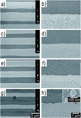
SEM images of the as grown regions are shown in the Fig. 1. Metal is close to percolation limit in the lowest [Au] sample and metal coverage increases in the range of 88–99% as the [Au] increases, as expected. Images of fringes having a period of 6.8 μm are shown in Fig. 2, where areas with different morphologies can be observed. The contrast of the bright areas is identical to that of the as grown regions and, therefore, it must be related to areas where the metal film remains. These bright regions will be referred to from now on as non-transformed regions and the dark regions as transformed regions. The latter are formed by round NPs that evidence that the laser exposure has induced the melting of the metal film. Due to the large surface energy difference between the glass and the metals, the liquid metal dewets and tends to form spheres. The mean diameter, ϕ, and number density of these NPs are homogeneous in the transformed region in the case of [Au] ≤ 52. However, NPs distribution in Fig. 2h shows a low concentration of big NPs (ϕ ∼ 100 nm) that are preferentially placed at the center of the transformed region. Magnified image of this transformed region shows that these big NPs are surrounded by a dense distribution of smaller NPs (see upper right inset in Fig. 2h). In addition, some nanostructures have been placed on the surface of the non-transformed region, and the interface between transformed and non-transformed region is blurred in comparison to the sharp interfaces that appears for [Au] ≤ 52. These morphological differences suggest the existence of at least two dewetting mechanisms as function of [Au]. Fig. 3a shows the mean diameter and NPs number density as a function of [Au]. In the case of [Au] = 60 only the larger NPs have been selected for the statistics. Mean diameter increases in the range of (64–110) nm and the NPs number density decreases in the range of (63–5) NPs μm−2 as [Au] increases. These results support that once the laser melts the metal, the mean size and size distribution of the NPs produced upon laser irradiation depends on the initial film thickness.28,29 Furthermore, we have demonstrated that homogeneous laser irradiation of bimetallic samples leads to alloyed NPs.30,31 Metal diffusion coefficients and metal thermal evolution during the laser pulse determines the production of alloy NPs. Ag and Au have high miscibility and inter-diffusion coefficient in the liquid state (typically in the 10−5 to 10−4 cm2 s−1 range32–34). Therefore, it is expected the complete mixing of the metal liquids produced by laser irradiation of nanosecond duration.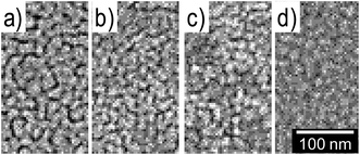 | ||
| Fig. 1 SEM images of as grown regions for the samples having (a) [Au] = 32, (b) [Au] = 40, (c) [Au] = 52 and (d) [Au] = 60. | ||
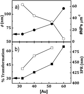 | ||
| Fig. 3 Evolution of several parameters of the fringes shown in Fig. 2 as a function of [Au]. (a) (●) Mean diameter of NPs in the transformed region and (○) their number density. (b) (■) Percentage of transformed region with respect to the period of the fringes, 6.8 μm and (□) SPR wavelength measured in the transformed region with the micro-hyper-spectral instrument. Full symbols are referred to left axis and open symbols to right axis. | ||
Layer thickness determines not only the size of the NPs but mainly the redistribution of the material in the transformed regions or the interface between transformed and non-transformed regions. NPs are homogeneously distributed in the transformed regions for [Au] ≤ 52 (Fig. 2b, d and f). However, a bimodal size distribution of close and small NPs and isolated ones which are placed preferentially at the center of the transformed region is evident for [Au] = 60 (Fig. 2h). In addition, the interfaces are sharp for [Au] ≤ 52 and they appear blurred for [Au] = 60. These morphological differences suggest the existence of at least two dewetting mechanisms as function of [Au]. Upon exposure of Au and Ag films to a single laser pulse of modulated beam intensity, melting and dewetting into isolated NPs, was reported as the main mechanism for film thicknesses thinner than some transitional value. When the thickness is higher than this value, the metal is transported from hot to cold regions by hydrodynamic flow of the liquid in the thermal gradient region producing the solidification and mass accumulation in the cold regions. This transitional thickness was estimated around 17 nm for Au and 20 nm for Ag films,35 which is in a good agreement with the metal thickness estimated for [Au] = 60 (Table 1). Therefore the hydrodynamic flow from hot to cold region allows us to explain the morphological features described for the thickest sample that appears in Fig. 2h. Furthermore, the presence of nanostructures on the surface of the non-transformed regions could be related to the metal liquid that flow from hot to cold regions that is detached from the upper part of the rims and placed on the non-transformed regions due to inertia of the rim.
Layer thickness and metal coverage determine also the ratio between transformed and non-transformed regions. Briefly, the transformed regions correspond to areas whose temperature reaches the melting threshold of the metals.36 Temperature of the film during the laser pulse depends on metal coverage and thickness that is comparable to the penetration depth, 18 nm for Ag and 8 nm for Au at λ = 193 nm. Thus, the amount of transformed regions must increase with [Au] as shown in Fig. 3b, where the percentage of transformed to non-transformed region normalized to the period increase in the range of 44–64% as [Au] increases. This result is in agreement with the reported elsewhere for homogeneous37 and laser interference38 laser irradiations in which the threshold fluence of transformation decreases as the metal thickness increases.
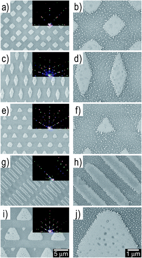
3.2 Morphology of 2D patterns
Left hand images in Fig. 4 show 2D patterns in the sample [Au] = 32 produced by the accumulation of two (squares, diamonds and rectangles) or three (triangles) laser pulses with different phase mask orientations (see Table 2 for details). The images on the right hand side correspond to high magnification images centered in the motif. Patterns of Fig. 4a–f have been produced with the projection optics that generates fringes with a period of 3 μm and different phase mask orientations and pulses numbers. Areas of non-transformed regions are reduced for each laser pulse, and thus, they are shaped like a square, diamond or triangle that are periodically distributed. These motifs are well defined for these three cases. Moreover, the small angle (40°) in the diamond (Fig. 4d) has been satisfactorily produced. This high resolution is related with the quality of the border between the transformed and non-transformed regions. All these motifs have a sharp interface that is related to the negligible mass transport from hot to cold region as discussed previously in the case of fringes (Fig. 2a and b). Transformed regions are covered by round NPs homogeneously distributed despite some transformed regions have been irradiated two times with fluences above the transformation threshold due to the geometric construction of the pattern. Shape and distribution of the NPs can be modified by accumulation of successive laser pulses.39 In a similar work, the nanostructures evolve from elongated to round in the regions irradiated with two pulses, but this effect is negligible in the present work due to the initial round shape of the NPs.38 Fig. 4i and e shows the patterns produced by a sequence of three laser pulses with periods of 3.0 μm and 6.8 μm respectively and a relative angle of 60°, thus a hexagonal lattice is formed. In this case the orientation of the phase mask is a critical point and a misalignment <0.2° produces that the motive evolves from triangles to hexagons in a distance of five hundred microns on the surface of the sample for Δ = 6.8 μm. This angular precision is lower than the experimental resolution in this experiment and thus different motifs from triangles to hexagons are formed along the irradiated region. Fig. 4i shows a motif formed by small and large quasi-triangles. One of these large structures is magnified in Fig. 4j, where the corners of these structures depend not only on the mass transport or [Au] but mainly to the motif that is periodically replicated, in this case large and small pseudo-triangles. In addition, shape of the motifs can vary slightly in few microns. For example, some quasi-hexagons surrounded by triangles are distinguishable in Fig. 4e. The origin of this slightly inhomogeneity in the shape of the motif in a short range scale at this stage is unclear. It might be related to the double frequency effects related to the Talbot effect.40 However, these effects have not appreciable consequences in the diffraction patterns of these structures.PMLI technique is a time-efficient and versatile technique that allows patterns with different periods to be generated. The pattern in Fig. 4g and h has been produced by two successive laser pulses with periodicities of 6.8 μm and 1.7 μm, and a relative phase mask orientation of 90°. Non-transformed rectangles have an area of 5 × 0.8 μm2 and their corners are rounded with a radius of ∼350 nm. Minimum period achievable with this technique depends not only but mainly on the initial morphology of the sample. Furthermore, rectangles as shown in Fig. 4g and h and other motifs with a period of 1.7 μm have a poor definition or vanish altogether for [Au] = 60, since, mainly in the case of thermally continuous layers, lateral heat diffusion from hot to cold regions limits the period achievable because the difference of threshold and full transformation fluence is reduced as period decreases.41
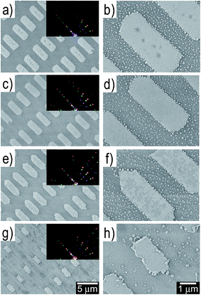
Fig. 5 shows a sequence of patterns produced with a fixed interfering configuration but different [Au]. The first pulse has a period of 6.8 μm and the second, with a relative phase mask orientation of 90°, has a period of 3 μm. Right hand side images in Fig. 5 show that the size of the non-transformed rectangle decreases as [Au] increases, since the threshold fluence of the transformation decreases as [Au] increases as discussed previously. In addition, resolution of the rectangles is deteriorated as [Au] increases. The long sides are well defined in all cases. However, the short sides and the vertex become less resolved as [Au] increases. Indeed, short sides present triangular shapes in the case of [Au] = 52 (Fig. 5f). This resolution loss must be related to the increase of thermal conductivity as [Au] increase, since the definition of the interface between transformed and non-transformed regions is blurred as the thermal conductivity increases.36,38 In the case of [Au] = 60, big NPs are heterogeneously distributed in the transformed regions and there is mass accumulation at the interface between the transformed and non-transformed region. These processes also have been identified and discussed previously in the case of fringes (Fig. 2h).
3.3 Optical response of fringes
The insets images on the left column in Fig. 2 show the spectral and angular distributions of the light diffracted by the corresponding fringes illuminated by the three lasers beams. Zeroth-order, at the bottom of the image, was attenuated within a neutral density filter, and the positions of the diffraction orders, m, are consistent with the grating period, Δ, angle of incidence, θin, and scattering angle, θout, described by the grating equation:
sin![[thin space (1/6-em)]](https://www.rsc.org/images/entities/char_2009.gif) θout = mλ/Δ − sin θout = mλ/Δ − sin![[thin space (1/6-em)]](https://www.rsc.org/images/entities/char_2009.gif) θin θin
| (1) |
In addition, the comparison of diffraction patterns clearly shows that diffraction efficiency depends on [Au]. The brightest diffraction orders appear for [Au] = 52, (inset in Fig. 2e). For instance, the third diffraction order (top of the images) is clearly visible for [Au] = 60 (inset of Fig. 2g), but not for [Au] = 32 (inset of Fig. 2a). In order to understand these dependences, the diffraction efficiency of the first diffraction order has been thoroughly analyzed.
Spectral diffuse reflectance measurements of these fringes are shown in Fig. 6. They were done at different scattering angles with respect to the zeroth-order direction, θ, always within the incidence plane, since the gratings were illuminated perpendicularly to the lines. It is observed that the spectral distribution moves toward longer wavelengths for higher scattering angles, following the grating equation (eqn (1)). However, there is definitively a difference in the intensity and trend of the absolute value of these peaks, which is crucial for the diffraction efficiency and colour produced by these gratings. The highest signal in the range (550–750) nm is obtained for [Au] = 52, being almost twice as high as [Au] = 60 and [Au] = 40 and four times more than that [Au] = 32. In addition, the spectral trends also vary with [Au]. Fig. 7 shows the peak intensity for each spectrum relative to the value at 750 nm. The plot clearly shows that the spectral trend of these peaks increases for [Au] = 60, decreases for [Au] = 32 while it keeps approximately constant for [Au] = 40 and [Au] = 52 in the range (550–750) nm as the wavelength increases.
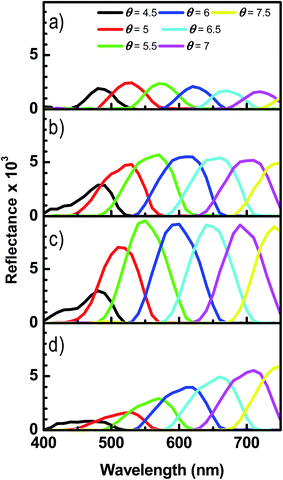 | ||
| Fig. 6 Spectra of light diffracted by the fringes shown in Fig. 2 of the (a) [Au] = 32, (b) [Au] = 40, (c) [Au] = 52 and (d) [Au] = 60 samples. Incident angle was set to 30° and the diffracted angle (θ) refer to the specular reflection. | ||
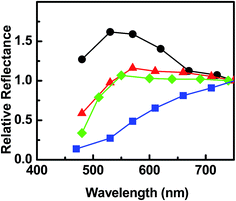 | ||
Fig. 7 Relative maximum intensity of the diffracted spectra shown in Fig. 6 normalized to 750 nm for the samples having ( ) [Au] = 32, ( ) [Au] = 32, ( ) [Au] = 40, ( ) [Au] = 40, ( ) [Au] = 52 and ( ) [Au] = 52 and ( ) [Au] = 60. ) [Au] = 60. | ||
The data represented in Fig. 6 and 7 reveal that the diffraction efficiency of the first diffraction order and its spectral dependence can be tuned in a broad range by varying [Au]. In the case of periodic structures without topography, such as patterns analyzed here, the ratio between transformed and non-transformed regions and their optical properties determines the diffraction efficiency.21,42 The former can modify the relative efficiency between different diffraction orders and the latter defines the optical contrast between the fringes. This last parameter is particularly relevant in these fringes since the optical constants of the alloy NPs are very different from those of as grown regions. In order to understand the relevance of the contrast, we measured the optical transmittance at normal incidence of those fringes with micrometric resolution using the micro-hyper-spectral system. Fig. 8 shows the transmittance of the non-transformed regions and the region transformed into NPs in the fringes analyzed in the Fig. 2. The transmittance spectra of non-transformed regions are consistent with the morphological structure of the as grown regions since they show a low transmittance band (absorption band) with a minimum in the range (500–700) nm for [Au] = 32, 40 and 52 associated to the percolation and the discontinuous character of the film (Fig. 1a–c), while they decrease quasi-linearly in the range (475–750) nm for [Au] = 60, consistently with the quasi-continuous metallic film (Fig. 1d). Transformed regions are more transparent in the whole visible range, their spectra have a high transmission in the IR and show a clear absorption peak in the range (430–485) nm for [Au] ≤ 52, which must be related to SPR of the alloy NPs. The main changes in the SPR are increases of the width and absorption peak intensity, and shift to red as [Au] increases (see Fig. 3b). These results are consistent with those reported elsewhere for alloy NPs, where the peak evolves from blue to green and broads as [Au] increases.30,31,43,44 In addition, Ag is the metal exhibiting the best plasmonic response, however the SPR for [Au] = 32 is weaker than that for [Au] = 52. It might be most likely related to the fact that the increase of [Au] in this work goes along with an increase of the total layer thickness, and thus the amount of metal transformed into NPs. In addition, absorption is not negligible for wavelengths higher than 500 nm in the case of [Au] = 60. This is consistent with the presence of close and small NPs in the transformed regions (see inset in Fig. 2h). In this case, the SPR changes and the plasmonic response is dominated by the balance between the inter-band transitions onset of the alloy NPs and the multipolar interaction among neighboring NPs. This broadband plasmonic response has been identified for similar NPs distributions produced by homogeneous laser irradiation of noble metal thin films.25,30
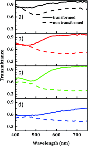 | ||
| Fig. 8 Transmittance of the transformed (full lines) and non-transformed region (dashed lines) of the fringes shown in Fig. 2 for the samples having (a) [Au] = 32, (b) [Au] = 40, (c) [Au] = 52 and (d) [Au] = 60. | ||
Difference between the transmittance at normal incidence of the region transformed into NPs, TNPs, and the non-transformed regions, TNonTr, in the fringes must be somehow related to the diffraction efficiency measured in reflection configuration. Simulation of the diffraction efficiency by using the optical parameters measured in the fringes requires complex algorithms45 and is beyond the scope of this work. As a rough estimation, we assume that the diffraction efficiency must be proportional to the optical contrast between the fringes, C, defined as C = (TNPs − TNonTr)/(TNPs + TNonTr). In order to find support of this hypothesis, the optical contrasts are plot (left y-axis) in Fig. 9 and the peak intensity of the diffuse reflectance spectra shown as a function of wavelength for the analyzed fringes in Fig. 7 (right y-axis). The relation factor between the two y-axes is the same for all the regions analyzed. The observed correlation of these two parameters shows a good agreement, especially in the case of [Au] = 32 and [Au] = 60. Nevertheless, the absolute values and the spectral trends are reasonably well estimated in the range (550–750) nm for all the [Au] values. Therefore, we conclude that the diffraction efficiency of the first diffraction order is mainly determined by the optical properties of the as grown region and regions transformed into NPs, the latter being characterized by their plasmonic response. This conclusion confirms the result obtained in a similar work of Au NPs gratings produced by two-beam laser interference, where the first order diffraction efficiency was affected by the average size, shape, and even the population distribution of Au NPs.46
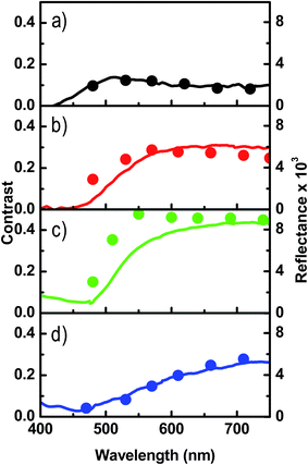 | ||
| Fig. 9 Optical contrast of the transformed and non-transformed regions of the fringes shown in Fig. 2. Dots indicate maximum intensity of the diffracted spectra shown in Fig. 6 for the samples having (a) [Au] = 32, (b) [Au] = 40, (c) [Au] = 52 and (d) [Au] = 60. The ranges of y-values are the same for all the images. | ||
3.4 Optical response of 2D patterns
Diffraction patterns of the bidimensional structures (insets in Fig. 4 and 5) show a great number of diffraction orders, which can be explained by using the Fraunhofer diffraction equations. The positions of the diffraction orders depend, basically, on the spatial distribution of the motifs. In a fast and precise way, the diffraction pattern can be obtained by calculating the Fourier transform of the images that shows the patterns.47 In some case a simplified estimation is enough to obtain the spatial distribution of the diffraction orders. For instance, in the case of square or rectangular lattices with periods X and Y, the spatial distributions of the motifs in the x,y plane can be described by the next equation:
 | (2) |
In addition the diffraction efficiency of the 2D pattern depends on the [Au] (as shown in the insets of Fig. 5). For instance, the diffraction orders of the rectangles for [Au] = 32 (Fig. 5a) are less intense than those for [Au] = 52. The agreement between these results and the previous analysis of the optical contrast, where the fringes of the [Au] = 52 samples have the highest diffraction efficiency, evidence that as a first approximation the intensity of the diffraction bidimensional pattern also is mainly determined by the morphology of the as grown regions and the plasmonic response of the NPs, although the shape and size of non-transformed region could modify the relative intensity of the diffraction orders. Even some of the diffraction orders can be completely attenuated depending on the type of motif that is replicated as is shown in the insets of Fig. 5, where some orders disappear, despite the motifs of Fig. 5a–h are arranged within the same spatial distribution that can be described by eqn (2).
Position and intensity of the diffraction patterns can be easily controlled by the laser pulse sequence and the [Au]. Therefore, a great variety of diffraction patterns can be produced by using this versatile technique. Customized and personalized diffraction patterns have a high potential for applications related to personal identification according with the quest of the enhanced police security. In addition, the characterization of these patterns does not require complex instrumentation for the surface analysis, since a simple continuous laser and a camera are only needed for the production, acquisition and identification of the unique diffraction pattern produced by the micrometric periodic structure. On the other hand, the PMLI technique is a fast and cheap approach having the capability to produce patterns over large areas in a time efficient and single-step process for producing personalized colour coatings through the unique associated diffraction pattern.
4. Conclusions
This work shows that a great variety of periodic structures with customized diffraction efficiency can be fabricated in Au/Ag films by using the PMLI technique. The motif is formed by non-transformed regions that preserve the initial as grown morphology, placed at the minimum of interference, surrounded by regions placed at the maximum of interference and transformed into alloy NPs due to the laser induced dewetting process. Mean diameter of the NPs and the percentage of transformed region increase with the gold concentration, [Au]. However, the thickest sample, with the highest [Au], shows a bimodal size distribution. The transition between the transformed and non-transformed regions is blurred for [Au] = 60 by the hydrodynamic flow and mass transport from hot to cold region. This process limits the resolution of the non-transformed areas and the minimum period achievable, which was in the range (3–1.7) μm for the sample with the highest [Au]. On the other hand, well defined fringes, squares and diamonds or rectangles with width of only 800 nm have been sculpted for the lowest [Au], which has the lowest thermal conductivity.In all cases, the optical response of the transformed regions is dominated by a plasmonic response associated to the alloy NPs. The weak plasmonic peak is enhanced, broadened and shifted to red as [Au] increases according to the morphological and alloy variations of the NPs in the transformed regions. In the case of the highest [Au] the plasmonic response shows an extra broadening in the IR region related with the multipolar interaction between the close NPs.
All the periodic structures analyzed show a clear diffraction pattern whose brightness can easily be varied by changing [Au]. In the case of fringes, the diffraction efficiency of the first order, for a given wavelength, can be magnified by a factor 4, or their dependence on the wavelength can decrease or increase depending on [Au]. Optical measurements demonstrate that these effects are related to the optical contrast between the non-transformed region and the region transformed into alloy NPs characterized by their plasmonic response.
Acknowledgements
We wish to express our deep gratitude to Prof. C. N. Afonso for their advices, comments and encouragement on the study from which this paper is derived and Prof. R. Serna for their valuable explanations of the ellipsometer use. R. J. Peláez acknowledges grant no. JCI-2012-13034 from the Juan de la Cierva program. A. Ferrero, B. Bernad and J. Campos are grateful to the Comunidad de Madrid for funding the program SINFOTON-CM: S2013/MIT-2790.References
- T. Xu, H. Shi, Y.-K. Wu, A. F. Kaplan, J. G. Ok and L. J. Guo, Structural Colors: From Plasmonic to Carbon Nanostructures, Small, 2011, 7(22), 3128–3136 CrossRef CAS PubMed.
- J. Huang, X. Wang and Z. L. Wang, Controlled Replication of Butterfly Wings for Achieving Tunable Photonic Properties, Nano Lett., 2006, 6(10), 2325–2331 CrossRef CAS PubMed.
- M. Khorasaninejad, N. Abedzadeh, J. Walia, S. Patchett and S. S. Saini, Color Matrix Refractive Index Sensors Using Coupled Vertical Silicon Nanowire Arrays, Nano Lett., 2012, 12(8), 4228–4234 CrossRef CAS PubMed.
- Y. Gu, L. Zhang, J. K. W. Yang, S. P. Yeo and C.-W. Qiu, Color Generation via Subwavelength Plasmonic Nanostructures, Nanoscale, 2015, 7(15), 6409–6419 RSC.
- U. Kreibig and M. Vollmer, Optical Properties of Metal Clusters, Springer-Verlag, 1995, p. 25 Search PubMed.
- M. Tsai, T. Liu, C. Tsen and C. Ting, Polarization Sensitivity of Light Diffraction for Periodic Array of Anisotropic Gold Nanoparticles, Appl. Phys. Lett., 2015, 106(24), 241107 CrossRef.
- C. L. Wong and M. Olivo, Surface Plasmon Resonance Imaging Sensors: A Review, Plasmonics, 2014, 9(4), 809–824 CrossRef CAS.
- K.-L. Lee, P.-W. Chen, S.-H. Wu, J.-B. Huang, S.-Y. Yang and P.-K. Wei, Enhancing Surface Plasmon Detection Using Template-Stripped Gold Nanoslit Arrays on Plastic Films, ACS Nano, 2012, 6(4), 2931–2939 CrossRef CAS PubMed.
- M. A. Schmidt, D. Y. Lei, L. Wondraczek, V. Nazabal and S. A. Maier, Hybrid Nanoparticle–Microcavity-Based Plasmonic Nanosensors with Improved Detection Resolution and Extended Remote-Sensing Ability, Nat. Commun., 2012, 3, 1108 CrossRef PubMed.
- G. Das, E. Battista, G. Manzo, F. Causa, P. A. Netti and E. Di Fabrizio, Large-Scale Plasmonic Nanocones Array For Spectroscopy Detection, ACS Appl. Mater. Interfaces, 2015, 7(42), 23597–23604 CAS.
- B. Yan, A. Thubagere, W. R. Premasiri, L. D. Ziegler, L. Dal Negro and B. M. Reinhard, Engineered SERS Substrates with Multiscale Signal Enhancement: Nanoparticle Cluster Arrays, ACS Nano, 2009, 3(5), 1190–1202 CrossRef CAS PubMed.
- M. Panagopoulou, N. Pantiskos, P. Photopoulos, J. Tang, D. Tsoukalas and Y. S. Raptis, Raman Enhancement of Rhodamine Adsorbed on Ag Nanoparticles Self-Assembled into Nanowire-like Arrays, Nanoscale Res. Lett., 2011, 6(1), 629 CrossRef PubMed.
- I. E. Sendroiu and R. M. Corn, Nanoparticle Diffraction Gratings for DNA Detection on Photopatterned Glass Substrates, Biointerphases, 2008, 3(3), FD23 CrossRef PubMed.
- M. E. Stewart, N. H. Mack, V. Malyarchuk, J. A. N. T. Soares, T.-W. Lee, S. K. Gray, R. G. Nuzzo and J. A. Rogers, Quantitative Multispectral Biosensing and 1D Imaging Using Quasi-3D Plasmonic Crystals, Proc. Natl. Acad. Sci. U. S. A., 2006, 103(46), 17143–17148 CrossRef CAS PubMed.
- T. Ellenbogen, K. Seo and K. B. Crozier, Chromatic Plasmonic Polarizers for Active Visible Color Filtering and Polarimetry, Nano Lett., 2012, 12(2), 1026–1031 CrossRef CAS PubMed.
- X. M. Goh, Y. Zheng, S. J. Tan, L. Zhang, K. Kumar, C.-W. Qiu and J. K. W. Yang, Three-Dimensional Plasmonic Stereoscopic Prints in Full Colour, Nat. Commun., 2014, 5, 5361 CrossRef CAS PubMed.
- X. Zhu, C. Vannahme, E. Højlund-Nielsen, N. A. Mortensen and A. Kristensen, Plasmonic Colour Laser Printing, Nat. Nanotechnol., 2015, 11(4), 325–329 CrossRef PubMed.
- S. J. Tan, L. Zhang, D. Zhu, X. M. Goh, Y. M. Wang, K. Kumar, C.-W. Qiu and J. K. W. Yang, Plasmonic Color Palettes for Photorealistic Printing with Aluminum Nanostructures, Nano Lett., 2014, 14(7), 4023–4029 CrossRef CAS PubMed.
- https://www.ec.europa.eu/programmes/horizon2020/.
- N. C. Lindquist, P. Nagpal, K. M. McPeak, D. J. Norris and S.-H. Oh, Engineering Metallic Nanostructures for Plasmonics and Nanophotonics, Rep. Prog. Phys., 2012, 75(3), 036501 CrossRef PubMed.
- Sudheer, S. Porwal, S. Bhartiya, B. T. Rao, P. Tiwari, H. Srivastava, T. K. Sharma, V. N. Rai, A. K. Srivastava and P. A. Naik, Diffraction Efficiency of Plasmonic Gratings Fabricated by Electron Beam Lithography Using a Silver Halide Film, J. Appl. Phys., 2016, 120(4), 043101 CrossRef.
- S. Indrišiūnas, B. Voisiat, M. Gedvilas and G. Račiukaitis, Two Complementary Ways of Thin-Metal-Film Patterning Using Laser Beam Interference and Direct Ablation, J. Micromech. Microeng., 2013, 23(9), 095034 CrossRef.
- T. Kunze, C. Zwahr, B. Krupop, S. Alamri, F. Rößler and A. F. Lasagni, Development of a Scanner-Based Direct Laser Interference Patterning Optical Head: New Surface Structuring Opportunities, Proc. SPIE, 2017, 1009214–1009217 Search PubMed.
- S. Riedel, M. Schmotz, P. Leiderer and J. Boneberg, Nanostructuring of Thin Films by Ns Pulsed Laser Interference, Appl. Phys. A, 2010, 101(2), 309–312 CrossRef CAS.
- C. E. Rodríguez, R. J. Peláez, C. N. Afonso, S. Riedel, P. Leiderer, D. Jimenez-Rey and A. C. Font, Plasmonic Response and Transformation Mechanism upon Single Laser Exposure of Metal Discontinuous Films, Appl. Surf. Sci., 2014, 302, 32–36 CrossRef.
- Y. Yamamura and H. Tawara, Energy Dependence of Ion-Induced Sputtering Yields From Monatomic Solids at Normal Incidence, At. Data Nucl. Data Tables, 1996, 62(2), 149–253 CrossRef CAS.
- G. Baraldi, A. Perea and C. N. Afonso, Dynamics of Ions Produced by Laser Ablation of Several Metals at 193 nm, J. Appl. Phys., 2011, 109(4), 043302 CrossRef.
- R. J. Peláez, G. Baraldi, C. N. Afonso, S. Riedel, J. Boneberg and P. Leiderer, Selective Gold Nanoparticles Formation by Pulsed Laser Interference, Appl. Surf. Sci., 2012, 258(23), 9223–9227 CrossRef.
- R. J. Peláez, C. N. Afonso, J. Bulíř, J. Lančok and M. Novotný, Diffractive and Coloured Films by Laser Interferometry Patterning, Surf. Coat. Technol., 2012, 211, 205–208 CrossRef.
- R. J. Peláez, C. E. Rodríguez, C. N. Afonso and M. Škereň, Tuning the Plasmonic Response of Bimetallic Films by Laser Irradiation, Surf. Coat. Technol., 2016, 295, 54–59 CrossRef.
- R. J. Peláez, C. E. Rodríguez and C. N. Afonso, Expanding the Plasmonic Response of Bimetallic Nanoparticles by Laser Seeding, Nanotechnology, 2016, 27(10), 105301 CrossRef PubMed.
- C. Gonella, A. Blanchet and J. Le Ny, A Method for Measuring the Interdiffusion Coefficient in a Liquid Metal Alloy. Application to the Binary Alloy Ag–Au, High. Temp. High Press., 1999, 31, 381–384 CAS.
- Surface Modification and Alloying by Laser, Ions, and Electron Beams, ed. J. M. Poate, G. Foti and D. C. Jacobson, 1983 Search PubMed.
- F. Ruffino, V. Torrisi, R. Grillo, G. Cacciato, M. Zimbone, G. Piccitto and M. G. Grimaldi, Nanoporous Au Structures by Dealloying Au/Ag Thermal- or Laser-Dewetted Bilayers on Surfaces, Superlattices Microstruct., 2017, 103, 28–47 CrossRef CAS.
- Y. S. Kaganovskii, Fabrication of Periodic Structures in Thin Metal Films by Pulsed Laser Irradiation, J. Nanophotonics, 2007, 1(1), 011690 CrossRef.
- R. J. Peláez, C. N. Afonso, M. Škereň and J. Bulíř, Importance of Layer Thermal Conductivity on the Sharpness of Patterns Produced by Laser Interference, Appl. Surf. Sci., 2016, 374, 61–64 CrossRef.
- S. J. Henley, J. D. Carey and S. R. P. Silva, Pulsed-Laser-Induced Nanoscale Island Formation in Thin Metal-on-Oxide Films, Phys. Rev. B: Condens. Matter Mater. Phys., 2005, 72(19), 195408 CrossRef.
- R. J. Peláez, C. N. Afonso, J. Bulíř, M. Novotný, J. Lančok and K. Piksová, 2D Plasmonic and Diffractive Structures with Sharp Features by UV Laser Patterning, Nanotechnology, 2013, 24(9), 095301 CrossRef PubMed.
- N. Kalfagiannis, A. Siozios, D. V. Bellas, D. Toliopoulos, L. Bowen, N. Pliatsikas, W. M. Cranton, C. Kosmidis, D. C. Koutsogeorgis, E. Lidorikis and P. Patsalas, Selective Modification of Nanoparticle Arrays by Laser-Induced Self Assembly (MONA-LISA): Putting Control into Bottom-up Plasmonic Nanostructuring, Nanoscale, 2016, 8(15), 8236–8244 RSC.
- A. Isoyan, F. Jiang, Y. C. Cheng, F. Cerrina, P. Wachulak, L. Urbanski, J. Rocca, C. Menoni and M. Marconi, Talbot Lithography: Self-Imaging of Complex Structures, J. Vac. Sci. Technol., B: Microelectron. Nanometer Struct., 2009, 27(6), 2931 CrossRef CAS.
- R. J. Peláez, C. N. Afonso, M. Škereň and J. Bulíř, Period Dependence of Laser Induced Patterns in Metal Films, Nanotechnology, 2015, 26(1), 015302 CrossRef PubMed.
- E. Popov, Gratings: Theory and Numeric Applications, Marseille: Institut Fresnel/CNRS/AMU, 2012 Search PubMed.
- R. Ferrando, J. Jellinek and R. L. Johnston, Nanoalloys: From Theory to Applications of Alloy Clusters and Nanoparticles, Chem. Rev., 2008, 108(3), 845–910 CrossRef CAS PubMed.
- S. K. Cha, J. H. Mun, T. Chang, S. Y. Kim, J. Y. Kim, H. M. Jin, J. Y. Lee, J. Shin, K. H. Kim and S. O. Kim, Au–Ag Core–Shell Nanoparticle Array by Block Copolymer Lithography for Synergistic Broadband Plasmonic Properties, ACS Nano, 2015, 9(5), 5536–5543 CrossRef CAS PubMed.
- M. H. Madsen and P.-E. Hansen, Scatterometry—Fast and Robust Measurements of Nano-Textured Surfaces, Surf. Topogr.: Metrol. Prop., 2016, 4(2), 023003 CrossRef.
- W.-C. Hung, W.-H. Cheng, M.-S. Tsai, W.-C. Chung, I.-M. Jiang and P. Yeh, Laser Pulse Induced Gold Nanoparticle Gratings, Appl. Phys. Lett., 2008, 93(6), 061109 CrossRef.
- J. W. Goodman, Introduction to Fourier Optics, McGraw-Hil., 1996 Search PubMed.
| This journal is © The Royal Society of Chemistry 2017 |

