
 Open Access Article
 This Open Access Article is licensed under a
 Creative Commons Attribution 3.0 Unported Licence
Anisotropic atomic-structure related anomalous Hall resistance in few-layer black phosphorus
T. Makinoa,
Y. Katagiria,
C. Ohataa,
K. Nomuraa and
J. Haruyama*b
aFaculty of Science and Engineering, Aoyama Gakuin University, 5-10-1 Fuchinobe, Sagamihara, Kanagawa 252-5258, Japan. E-mail: J-haru@ee.aoyama.ac.jp
bInstitute for Solid State Physics, The University of Tokyo, 5-1-5 Kashiwanoha, Kashiwa, Chiba 277-8581, Japan
First published on 27th April 2017
Abstract
Mono- (or few) layer black phosphorus (BP) is highly expected to be a next-generation two-dimensional (2D) atom-thin semiconductor. Compared with other 2D atom-thin layers, BP has a significantly anisotropic atomic structure, which can provide unique electronic, optical, and magnetic properties. Herein, we report the observation of B2/3 magnetic-field (B) dependence of the Hall resistance with extremely small quantized levels in the low-B regime of the few-layer BP, which are associated with the anisotropic electronic structure confirmed by largely anisotropic hole mobilities. One of the qualitative interpretations for the B2/3 dependence is the possible presence of a uniaxial Dirac spectrum (arising from a closed band gap caused by uniaxial stretch along the buckling armchair direction, which is occasionally introduced by a process for cutting and wire-bonding samples, confirmed by Raman spectroscopy) and its hybridization with a Schrödinger spectrum existing along a zigzag direction. The observed phenomena imply significant potential due to strong anisotropy of atom-thin (few-layer) BP, which is highly expected to open doors to novel physics and its application for innovative 2D atom-thin devices.
Introduction
Among the large family of 2D atom-thin materials, mono(few)-layer BP has appeared as a 2D semiconductor with a substantial energy band gap intermediating between the zero-gap graphene and the large band-gap of the transition-metal dichalcogenide family.1–3,25 High carrier mobilities, μ, up to ∼4000 cm2 V−1 s−1 at low temperatures and Shubnikov–de Haas (SdH) oscillations have been demonstrated in few-layer BP with improved crystal quality resulting from the removal of impurities.3 Large edge-magnetism at room temperature has also been predicted and actually observed in oxygen-terminated BP nanoribbons and nanomeshes.4,5Highly in contrast to graphene, mono(few)-layer BP has a unique anisotropic atomic structure (Fig. 1(a); i.e., a zigzag structure within a monolayer along the y-axis and buckling armchair formed over two layers along the x-axis), which results in a puckered honeycomb lattice on a top view (Fig. 1(b)). It yields anisotropic electronic structures (e.g., electron effective mass m* and μ), which are very important for innovative electronic and optical device27 applications. As shown in Fig. 1(a) and (b), a puckered honeycomb lattice clearly provides the hopping integrals t ≠ t′ between the nearest neighbors because t and t′ for the in-plane zigzag and buckling armchair structures, respectively, are different. Indeed, |t| = 1.220 eV for the in-plane zigzag and t′ = 3.665 eV for the buckling armchair, with the m* several times lighter in the armchair than in the zigzag direction, and a strong angular dependence of the conductivity has been reported in mono(few)-layer BP.6–8,12,27
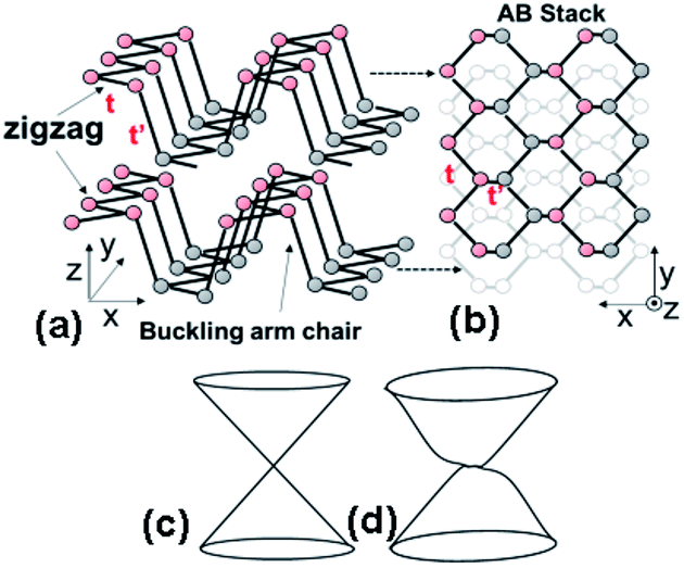 | ||
| Fig. 1 Schematic of (a) in-plane anisotropic atomic structure of BP (i.e., zigzag within monolayer along the y-axis and buckling armchair formed over two layers along the x-axis) and (b) a puckered honeycomb lattice on a top view. t and t′ are hopping integrals between nearest neighbors, corresponding to P-atoms within in-plane zigzag and buckling armchair over two layers, respectively. (c) and (d) examples of low energy spectrum for (c) t′ = t and (d) t′ = 2t in graphene. | ||
This t ≠ t′ yields unique B dependence of the Landau Levels (LLs) in graphene,14 in which the energy levels around the band center (E = 0) (with Dirac spectrum,15 Fig. 1(c)) vary with B as EN(B) ∼ ±(NB)1/2, with a twofold valley degeneracy.16 This B1/2-dependent spectrum is different from the well-known B dependence of LLs; EN(B) = (N + 1/2)eB/m* for electrons in a quadratic band with m* (i.e., Schrödinger spectrum). On the other hand, the novel B dependence of the LLs implying a power law, a [(N + γ)B]2/3 behaviour with γ = 1/2 arising from a hybridization of the Dirac and Schrödinger spectrum, has been theoretically reported recently for the specified graphene with t ≠ t′ (i.e., t′ = 2t; Fig. 1(d)) in the low B region of the Hofstadter–Rammal spectrum.14,26 The value γ = 1/2 results from the cancellation of a Berry phase.
Moreover, band gap closure resulting in the appearance of a Dirac cone28 has been recently reported in potassium-doped BP, exhibiting strong anisotropy (i.e., a Dirac semimetal state with a linear band dispersion in the armchair direction and a quadratic one in the zigzag direction),9,10 as well as band gap modulation caused by strain.11–13 Therefore, it is crucial to experimentally clarify how the anisotropic atomic structures yield further unique physical characteristics, which contribute to the applications for innovative electronic, optical, and magnetic devices in mono(few)-layer BPs.
Results and discussion
Sample characterization
Fig. 2(a) and (b) show optical and atomic force microscope images of a BP with top and cross sectional views, respectively. The samples have been fabricated by mechanical exfoliation of bulk BP (Smart Element Co.) on a clean SiO2/Si substrate, of which the surface was thoroughly cleaned mechanically and chemically (O2 plasma cleaning) before forming the BP in order to obtain high carrier mobility, following the Scotch tape method. Typical sample area and thickness are ∼400 μm2 and ∼4 nm, respectively.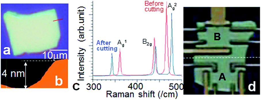 | ||
| Fig. 2 (a) Optical and (b) atomic force microscope images of a BP flake on top and cross sectional views, respectively. Panel (b) has been measured along red line shown in (a) (i.e., at a right edge of the flake). (c) Typical Raman spectrum of the (a) sample corresponding to sample A in (d). Red curve is the spectrum before cutting the substrate, and the blue curve is that after cutting the substrate into two individual substrates each with one Hall pattern, thinning, mounting on packages, and wire-bonding to the package by Au wires. (d) Optical microscope image of the sample with two Hall bar patterns with 90° different directions (A and B) used for electrical measurements. White dotted line between two regions is just a guide for the eyes. Each sample direction is not intentionally aligned to crystal orientations (x, y) shown in Fig. 1(a) and (b). As mentioned in (c), the substrate has been cut into two individual substrates for electrical measurements. | ||
After the mechanical exfoliation, the BP samples have been preserved in high-vacuum in order to avoid heavy oxidation. Fig. 2(d) shows an optical microscope image of the sample with two Hall bar patterns used for electrical measurements. Two Hall patterns have been fabricated on one BP substrate in different directions within 90° (i.e., main bars of samples A and B) in order to clarify the anisotropic electronic transport, although each sample direction is not intentionally aligned to crystal orientations (x, y) shown in Fig. 1(a) and (b). After this initial formation, the Si/SiO2 substrate has been mechanically cut by dicing into two individual substrates each with one Hall pattern. Then, the individual Si/SiO2 substrates have been thinned and mounted on packages for electrical measurements, and electrode pads have been bonded to the package by Au wires.
The red curve in Fig. 2(c) shows the Raman spectrum of the sample shown in Fig. 2(a) (sample A in (d)) before cutting the substrate, which agrees with that in few-layer BP. In contrast, the blue curve demonstrates the Raman spectrum after cutting this substrate into two individual substrates each with one Hall pattern by hand thinning, mounting on packages, and bonding to the package by Au wires (sample A in (d)). It implies a large shift of A1g and A2g peaks in opposite directions (i.e., 360 to 340 cm−1 (∼−1/18) for A1g and 465 to 480 cm−1 (∼1/31) for A2g). Ref. 24 gives the quantitative information for changes of Raman shift ratios caused by strain modulation (i.e., ∼−1/12, ∼1/22, and ∼1/15 for A1g, B2g, and A2g, respectively). Our results for A1g and A2g peaks are qualitatively consistent with those considering the opposite shift direction, although the shift values are smaller than those in ref. 24. On the other hand, the B2g peak is almost unchanged in Fig. 2(c). This is also consistent with the extremely small shift of the B2g peak against the applied strain because B2g mode originates from only lattice vibration in parallel with the substrate. Therefore, Fig. 2(c) suggests the introduction of a stretch mode (uniaxial strain) into few-layer BP, which should result in a closed band gap and subsequent appearance of the observed anisotropic Hall resistance (i.e., B2/3 dependence due to the closed band gap) as shown later.
Electrical properties
Fig. 3 shows examples of typical electrical properties of two samples. Fig. 3(a) shows the ohmic feature for a drain current (IDS) as a function of drain voltage (VDS) of sample A, whereas sample B shows much lower IDS. Interestingly, we find that field-effect mobility for the hole (μh), which is extracted from the line fit of the transfer characteristics (i.e., relationships for normalized conductance (G) vs. back gate voltage (Vbg)), has strong anisotropy as shown in Fig. 3(b) (sample A) and 3(c) (sample B). In sample A, μh is estimated to be ∼320 cm2 V−1 s−1 at T = 300 K and ∼3300 cm2 V−1 s−1 at T = 1.5 K (from dotted lines in Fig. 3(b)), whereas much smaller μh of ∼120 cm2 V−1 s−1 at T = 300 K is estimated in sample B (Fig. 3(c)). This μh of ∼3300 cm2 V−1 s−1 almost agrees with that of previous reports of BP, with the best quality reported in ref. 3, and it allows the possible observation of low-B (quantum) Hall resistances (particularly Rxy) at low temperatures. The abovementioned surface cleaning of the Si/SiO2 substrate and a thickness of ∼4 nm contribute to this high μh of sample A, as reported in ref. 8.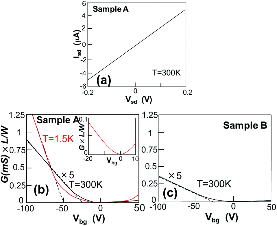 | ||
| Fig. 3 (a) Drain current (IDS) as a function of drain voltage (VDS) of sample A in Fig. 2(d). (b and c) Relationships for conductance (G) vs. back gate voltage (Vbg) normalized by channel length (L) and width (W) of samples A (b) and B (c). Dotted lines are for extraction of field-effect mobility. Inset of (b): expansion around Vbg = 0 of the main panel. | ||
These results suggest strong anisotropy in electronic structures, possibly associated with the anisotropic atomic structure of BP, when it is assumed that device orientations are occasionally aligned to the crystal orientations (i.e., directions of the main Hall bars (current channel) in samples A and B in Fig. 2(c) are aligned to the x-axis and y-axis in Fig. 1(a), respectively). Indeed, t′ = 3t has been reported in BP nanoribbons as mentioned above (e.g., |t| = 1.220 eV for in-plane zigzag and t′ = 3.665 eV for buckling armchair).6 This is exactly consistent with the observed anisotropic ratio of μh of ∼120/320 cm2 V−1 s−1 at T = 300 K. The m* value, which is several times smaller in the armchair direction and causes a larger μh to the armchair direction, has actually been reported previously. The ratio of μh of ∼120/320 cm2 V−1 s−1 is smaller than that of the angle-dependent conductivity ratio of ∼0.3/0.45 mS mm−1 reported in ref. 8. This also supports a stronger anisotropic electrical property in our sample due to the exact alignment of the Hall bar directions with the crystal directions as mentioned above. Moreover, the band gap closes (i.e., parabolic-like Vbg dependence) around Vbg = 0 in sample A, as observed in the inset of Fig. 3(b). This should be associated with uniaxial stretch mode as mentioned in later, although it is in contradiction to the presence of the band gap in conventional BP and unlike that of the Dirac point in graphene (i.e., linear Vbg dependence for band gap closing).
Fig. 4(a) exhibits Rxy observed in low-B Hall measurements in sample A. As B increases from B = 1.5 T, Rxy monotonically increases but shows three plateaus. The background, in which the mid B points of the individual plateaus are selected and combined (red dotted curve), follows B2/3 dependence rather than the linear B dependence (blue linear line). This is more evident in the inset, in which the x-axis corresponds to B2/3. In contrast, SdH oscillations are not evidently observed in Rxx in Fig. 4(a) owing to μh being smaller than that of ref. 3 and having a low-B measurement, although several small oscillations corresponding to the B for the transition regions between the plateaus in Rxy are observable. Moreover, the quantized Rxy values correspond to RQ (=h/e2 = 25.8 kΩ)/400–65 Ω between the N = 1 and N = 2 plateaus and RQ/200–130 Ω between the N = 2 and N = 3 plateaus and also the N = 3 and N = 4 plateaus. Such small quantization has also been observed in ref. 3. These resistance behaviours have been entirely smeared out above T ∼ 10 K. After heavy oxidation by exposing the sample in air atmosphere for one-half of a day, the Rxy changes to an electron-doped type, and the B2/3 relationship and these plateaus disappear (Fig. 4(b)).
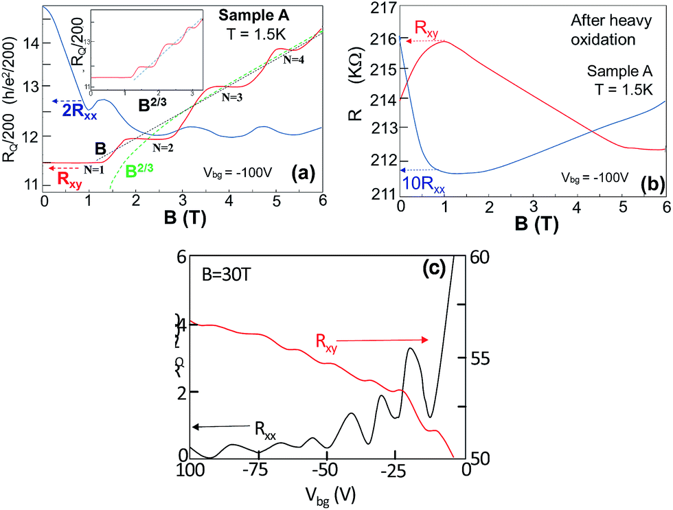 | ||
| Fig. 4 (a) Observed results in low-B Hall measurements of sample A, 2Rxx (blue curve) and Rxy (red curve). N noted for Rxy indicates the number of the plateaus. Green and black dotted curves correspond to data fit using B2/3 and B dependence, respectively. (b) Results of Hall measurements of sample A after heavy oxidation by exposing the sample to air atmosphere for one-half of a day, after the Hall measurements in (a). (c) Measurement result of Vbg dependence of Rxy and Rxx at a fixed high B (=30 T). | ||
A measurement result of Vbg dependence of Rxy and Rxx at a fixed high B (30 T) is shown in Fig. 4(c). It demonstrates that our system can possess LLs and SdH at high B, whereas the signature of the hybridization of Schrödinger and Dirac systems cannot be confirmed in such a high B region.
Discussion
We discuss the B2/3 dependence of Rxy and quantized values RQ/N (N = 200, 400) observed in Fig. 4(a). As mentioned in the introduction, B2/3 dependence of LL energy E has been predicted for the case of t ≠ t′ under low B. It predicts the presence of the E ∝ B2/3 relationship for each N value (node of edge states), i.e., E ∝ [(N + 1/2)B]2/3. Under a fixed chemical potential μc (i.e., fixed Vbg; blue dotted line in Fig. 5), an increase in Rxy with increasing B corresponds to a transition between N and (N + 1) LL modes in the E vs. [(N + 1/2)B]2/3 relationship (Fig. 5) and subsequent appearance of individual Rxy plateaus. Widths (i.e., period) of individual plateaus in Fig. 4(a) are determined by the B values for this transition between N and (N + 1) LL mode, which reflects the E vs. [(N + 1/2)B]2/3 relationship for individual N values (i.e., green curves along the B2/3 curves and red arrows along E = 0 in Fig. 5). Consequently, these B values corresponding to the distance between the mid B-points of individual plateaus as mentioned above and quantized values RQ/N (N = 200, 400) on the y-axis qualitatively display the observed B2/3 dependence of Rxy in Fig. 4(a).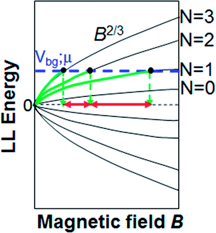 | ||
| Fig. 5 Schematic of LL energy E vs. B2/3 relationship at low B. Vbg (blue dotted line) indicates an example of position of the fixed chemical potential (μ). | ||
Quantitatively, LL energy En = (2πec/β(m)1/2)2/3[(N + γ)B]2/3 has been theoretically given in ref. 14, where c is the velocity of light and β = 4.94, resulting in the order of En ∼ 400[(N + 1/2)B]2/3. Assuming a fixed En = μ determined by a fixed Vbg, the plateau width should decrease with a ratio of (0.54/2.8) for (N = 1/N = 0) following this relationship (Fig. 5). On the contrary, the width ratio is almost half in Fig. 4(a), and the quantitative agreement is poor. Moreover, the confirmed anisotropy in μh as large as ∼120/320 cm2 V−1 s−1 at T = 300 K indicates the possibility for t′ = 3t. For the case of t′ > 2t, ref. 14 predicts that a crossover should appear between a quadratic and a quartic region. Therefore, further experimental and theoretical investigations are required for qualitative conclusion.
Mono (few)-layer BP has conventionally no Dirac cones (Dirac spectrum), whereas the closed band gap and subsequent appearance of the Dirac cone have been recently reported in potassium-doped BP, as mentioned above.9,10 It exhibited strong anisotropy (i.e., a Dirac semimetal state with a linear band dispersion in the armchair direction (for the Dirac spectrum) and a quadratic one in the zigzag direction (for the Schrödinger spectrum)). Moreover, under strong strain (stress, bending) and high electrical fields, similar band gap modulations have been reported.11–13,17 In the present case, introduction of strain has been confirmed by the Raman spectrum (Fig. 2(c)). The observed shift of A1g and A2g peaks corresponds to those in uniaxial stretch mode with ∼0.1ε along the armchair direction in BP.24 It is well known that cutting the SiO2/Si substrate and bonding the wafer of thinned substrates introduce such uniaxial strains (stress).18–21 On the other hand, closed band gap in BP is predicted by applying a uniaxial strain along the armchair direction (e.g., 0.1–0.16ε).13 The observed uniaxial stretch mode with ∼0.1ε along the armchair direction corresponds to this value, and thus, it implies the possibility of closed band gap along the armchair direction and subsequent emergence of a Dirac spectrum. It is approximately consistent with the closed band gap around Vbg = 0 shown in the inset of Fig. 3(b).
The observed quantized Rxy values ∼RQ/200 (or 400) are extremely small and the origin is not clear at this moment. These are attributed to neither quantum Hall effect (as mentioned above) nor universal conductance fluctuation (UCF), in which the root-mean-square (rms) amplitude of the fluctuation δG reaches the universal value ∼e2/h, when the sample size L ≪ both Lϕ (phase coherence length) and LT (thermal length). When either Lϕ or LT becomes smaller than L, the shorter of these governs the amplitude of fluctuations. The former corresponds to our case because of a small BP flake. In contrast, the observed small Rxy step is not fluctuation, and δG (i.e., conductance peak) cannot be defined. Even if we assume the Rxy step ∼RQ/200 as 1/δG, δG becomes ∼200 × (1/RQ). This value cannot be explained by the universal value ∼e2/h = 1/RQ.
Possibilities of similar t ≠ t′ relationship and subsequent appearance of B2/3 dependence of LLs in other systems have also been reported in the above-mentioned graphene within uniaxial stress (bending),17 2D organic conductors,22 and cold atoms in a laser-beam induced optical lattice.23 Strong anisotropic atomic structure of BP with t ≠ t′ may be favored to yield B2/3 dependence of LLs compared with these systems because of the presence of the t ≠ t′ relationship.
Conclusions
In conclusion, we have reported the observation of B2/3 dependence of Rxy with extremely small quantized levels, which are related to anisotropic electronic structure confirmed by strongly anisotropic μh in few-layer BP. Hybridization of a possible Dirac spectrum (arising from a closed band gap introduced by the uniaxial stretch along the armchair direction, which was confirmed by the Raman spectrum) and Schrödinger spectrum along the zigzag direction is one of the possible qualitative interpretations for the B2/3 dependence. We have found such unique characteristics only in a few samples to date, in which the current channel direction was occasionally aligned to the exact armchair direction and also the closed band gap was accidentally realized by uniaxial stretch mode through the Si/SiO2 substrate cutting and wire-bonding processes. Therefore, intentional fabrication of such samples as well as confirmation of the uniaxial Dirac spectrum and the values of t and t′ in oxidized BP is indispensable. Investigation of the case for mono-layer BP is also indispensable using a hBN substrate. Nevertheless, the observed phenomena are robust and imply significant potential due to strong and unique anisotropy of atom-thin (few-layer) BP, which is highly expected to open doors to novel physics and applications for innovative 2D atom-thin devices.Acknowledgements
The authors thank T. Nakamura, S. Katsumoto, Y. Shimazaki, M. Yamamoto, S. Tarucha, T. Enoki, A. H. Macdonald, P. Seneor, R. Wiesendanger, P. Herrero, P. Kim, and M. S. Dresselhaus for their technical contribution, fruitful discussions, and continuous encouragement. The study at Aoyama Gakuin was partly supported by a Grant-in-aid for Scientific Research (15K13277) in MEXT and AOARD grant (135049) in U.S. Air Force Office of Scientific Researches.Notes and references
- S. P. Koenig, R. A. Doganov, H. Schmidt, A. H. Castro Neto and B. Özyilmaz, Appl. Phys. Lett., 2014, 104, 103106 CrossRef.
- A. C. -Gomez, L. Vicarelli, E. Prada, J. O. Island, K. L. N. -Acharya, S. I. Blanter, D. J. Groenendijk, M. Buscema, G. A. Steele and J. V. Alvarez, 2D Materials, 2014, 1, 025001 CrossRef.
- L. Li, G. J. Ye, V. Tran, R. Fei, G. Chen, H. Wang, J. Wang, K. Watanabe, T. Taniguchi and L. Yang, et al., Nat. Nanotechnol., 2015, 10, 608–613 CrossRef CAS PubMed.
- Y. Nakanishi, R. Iwaki, D. Soriano, S. Roche, T. Nakamura, S. Katsumoto and J. Haruyama, Nano Res., 2016, 10, 718–728 CrossRef.
- Z. Zhu, C. Li, W. Yu, D. Chang, Q. Sun and Y. Jia, Appl. Phys. Lett., 2014, 105, 113105 CrossRef.
- A. N. Rudenko and M. I. Katsnelson, Phys. Rev. B: Condens. Matter Mater. Phys., 2014, 89, 201408 CrossRef.
- E. T. Sisakht, M. H. Zare and F. Fazileh, Phys. Rev. B: Condens. Matter Mater. Phys., 2015, 91, 085409 CrossRef.
- H. Liu, A. T. Neal, Z. Zhu, Z. Luo, X. Xu, D. Tománek and P. D. Ye, ACS Nano, 2014, 8, 4033–4041 CrossRef CAS PubMed.
- J. Kim, S. S. Baik, S. H. Ryu, Y. Sohn, S. Park, B.-G. Park, J. Denlinger, Y. Yi, H. J. Choi and K. S. Kim, Science, 2015, 349, 723 CrossRef CAS PubMed.
- S. S. Baik, K. S. Kim, Y. Yi and H. Joon Choi, Nano Lett., 2015, 15, 7788 CrossRef CAS PubMed.
- A. S. Rodin, A. Carvalho and A. H. Castro Neto, Phys. Rev. Lett., 2014, 112, 176801 CrossRef CAS PubMed.
- X. Peng, Q. Wei and A. Copple, Phys. Rev. B: Condens. Matter Mater. Phys., 2014, 90, 085402 CrossRef.
- Y. Li, S. Yang and J. J. Li, J. Phys. Chem. C, 2014, 118, 23970–23976 CAS.
- P. Dietl, F. Piéchon and G. Montambaux, Phys. Rev. Lett., 2008, 100, 236405 CrossRef PubMed.
- K. S. Novoselov, A. K. Geim, S. V. Morozov, D. Jiang, Y. Zhang, S. V. Dubonos, I. V. Grigorieva and A. A. Firsov, Science, 2004, 306, 666 CrossRef CAS PubMed.
- K. S. Novoselov, A. K. Geim, S. V. Morozov, D. Jiang, Y. Zhang, S. V. Dubonos, I. V. Grigorieva and A. A. Firsov, Nature, 2005, 438, 197 CrossRef CAS PubMed.
- R. Heyd, A. Charlier and E. McRae, Phys. Rev. B: Condens. Matter Mater. Phys., 1997, 55, 6820 CrossRef CAS.
- K. T. Turner, ECS Trans., 2008, 16, 321–328 CAS.
- W. N. Sharpe Jr, W. N. Sharpe Jr, J. Pulskamp, J. Pulskamp, D. S. Gianola, C. Eberl, C. Eberl, R. G. Polcawich, R. G. Polcawich and R. J. Thompson, Exp. Mech., 2006, 47, 649 CrossRef.
- S. L. Toh, K. P. Loh, C. B. Boothroyd, K. Li, C. H. Ang and L. Chan, J. Vac. Sci. Technol., B: Microelectron. Nanometer Struct.--Process., Meas., Phenom., 2005, 23.3, 940 CrossRef.
- S. Goel, A. Kovalchenko, A. Stukowski and G. Cross, Acta Biomater., 2016, 105, 464 CrossRef CAS.
- S. Katayama, A. Kobayashi and Y. Suzumura, J. Phys. Soc. Jpn., 2006, 75, 054705 CrossRef.
- E. Zhao and A. Paramekanti, Phys. Rev. Lett., 2006, 97, 230404 CrossRef PubMed.
- R. Fei and L. Yang, Appl. Phys. Lett., 2014, 105, 083120 CrossRef.
- Y. Katagiri, T. Nakamura, A. Ishii, C. Ohata, M. Hasegawa, S. Katsumoto, T. Cusati, A. Fortunelli, G. Iannaccone, G. Fiori, S. Roche and J. Haruyama, Nano Lett., 2016, 16, 3788 CrossRef CAS PubMed.
- Y. Hasegawa and M. Kohmoto, Phys. Rev. B: Condens. Matter Mater. Phys., 2006, 74, 155415 CrossRef.
- V. Tran, R. Soklaski, Y. Liang and L. Yan, Phys. Rev. B: Condens. Matter Mater. Phys., 2014, 89, 235319 CrossRef.
- R. Fei, V. Tran and L. Yang, Phys. Rev. B: Condens. Matter Mater. Phys., 2015, 91, 195319 CrossRef.
| This journal is © The Royal Society of Chemistry 2017 |