
 Open Access Article
 This Open Access Article is licensed under a Creative Commons Attribution-Non Commercial 3.0 Unported Licence
PDMS-based microfluidic devices using commoditized PCBs as masters with no specialized equipment required†
Jing Tu ,
Yi Qiao,
Haiqing Feng,
Junji Li,
Jiye Fu,
Fupeng Liang and
Zuhong Lu*
,
Yi Qiao,
Haiqing Feng,
Junji Li,
Jiye Fu,
Fupeng Liang and
Zuhong Lu*
State Key Laboratory of Bioelectronics, School of Biological Science and Medical Engineering, Southeast University, Nanjing, 210096, China. E-mail: zhlu@seu.edu.cn; Tel: +86-025-83793779
First published on 20th June 2017
Abstract
Designed printed circuit boards (PCBs) are alternative substrates for master mold construction of microfluidic devices. However, the rough supportive material molds rough replicas and causes difficulty in device sealing. To overcome this difficulty, a copper layer is used to generate a smooth surface. Some other researchers have used thermoplastic elastomers, which are typically much easier to bond, instead of the general polymer polydimethysiloxane (PDMS). This study presents an extremely simple approach for fabricating PDMS-based microfluidic devices using PCBs as masters. Unlike those reported in the previous studies, commoditized PCBs fabricated at a common PCB manufactory were directly used as the master molds. Two layers of semi-cured silicone of a distinct base to curing agent ratios were bonded together by additional curing. Efficient bonding was accomplished and avoided insufficient adhesion due to the rough surfaces of the PDMS replicas. Highly monodisperse droplets with polydispersity values smaller than 1% were stably formed using the easy fabricated devices. Essential operations in droplet microfluidics were reliably conducted in the PDMS-based devices. Moreover, the droplets were orderly sorted by the microstructures in the fabricated multi-height devices. The fabrication process provided a simple, convenient and reliable approach to prepare the general polymer PDMS-based microfluidic devices with a minimal requirement for equipment.
Introduction
Microfluidic technology significantly improves the speed, cost, efficiency and automation of analysis.1 Devices with microstructures have been widely applied2 in sample preparation,3,4 amplification improvement,5 droplet generation6 and operation,7,8 and cell culture9 and analysis.10 Microfluidic devices were made of silicon in the early stage.11 The requirement for specialized equipment and cleanrooms in silicon microfabrication limited the research activities in microfluidics. The development of soft lithography12–15 in the 1990s made microfluidics much more accessible than it had been previously.16 However, cleanroom facilities were still required for photolithography to produce the master.Designed printed circuit boards (PCBs) with constricted microstructures are alternative substrates for microfluidic devices17,18 and master mold construction.19,20 By selecting an appropriate copper layer thickness, microchannels at discrete and well-controlled heights ranging from 15 to 120 μm can be readily constructed with the PCB masters.21 The fabrication of PCBs does not need cleanroom facilities, making microfluidic technology easily accessible to several researchers in different fields.19 However, the rough supportive material (paper phenolic or glass epoxy) under the copper foil molds rough replicas, which cause difficulty in device sealing.19
In some studies,19,22,23 the copper layer was partially removed and washed and polished to mold polydimethysiloxane (PDMS) replicas against a smooth surface.19 After plasma treatment, the molded PDMS replicas could self-seal with glass slides. Appropriate modification is required in etching to partially retain the copper layer. It is well known that the copper layer is completely removed in electronic device preparation. Therefore, commoditized PCBs do not work for this method. Fabrication of the modified PCB masters depends on the researchers themselves. The procedure for preparing PCB masters is not complex, but requires some specialized equipment and active chemical reagents, which limits the method's application in the laboratories in different fields. In other studies, thermoplastic elastomers, such as styrene–ethylene/butylene–styrene triblock copolymer (SEBS), were used to achieve strong uniform bonds with glass or elastomer surfaces.20,24 The roughness of the PCB supportive material does not pose a problem for these melt-processable materials. Strong uniform bonds can be achieved by heating the material to a temperature just below its softening point20 or by hot embossing and chloroform vapour assisted bonding,24 alternatively. Although thermoplastic elastomers have some manufacturing advantages for flexible microfluidic systems, the thermosetting PDMS is more widely accepted and is the polymer of choice for rapidly prototyping polymer microfluidics.25 For the laboratories of different fields, PDMS is more familiar and practical than thermoplastic elastomers.
In this study, we present an extremely simple approach for fabricating PDMS-based microfluidic devices using PCBs as masters. Unlike those reported in the previous studies, commoditized PCBs were directly used in our study as the master molds of the PDMS microfluidic devices. Two layers of semi-cured silicone of distinct base to curing agent ratios were bonded together. At least one PDMS layer was molded against a PCB with constricted microstructures. Although the surfaces of the PDMS replicas molded against the commoditized PCBs are slightly rough, additional curing accomplished the bonding between the semi-cured layers and avoided insufficient adhesion. Almost no specialized equipment and facilities are required for the device fabrication. Using these easily fabricated PDMS devices, droplets with polydispersity values smaller than 1% were stably formed and delicately manipulated. A multi-height device was fabricated by bonding two PDMS replicas with microstructures for the passive sorting of droplets.
Experimental
PCB masters
The designs of the microfluidic structures were generated using the commonly used PCB drawing software (Protel, Altium Corporation, Hobart, Australia). The design documents were sent to a common PCB manufactory (Shunyijie Technology Corporation, Shenzhen, China), and the PCBs were fabricated using standard industrial etching techniques. The copper foil thickness of all the PCBs used in this study was 2 oz ft−2 (about 70 μm).Fabrication of the PDMS microfluidic devices
The procedure for preparing the microfluidic devices is described in Fig. 1. PDMS prepolymer and the curing agent (Sylgard 184, Dow Corning Corporation, Midland, MI, USA) were mixed at a ratio of 20![[thin space (1/6-em)]](https://www.rsc.org/images/entities/char_2009.gif) :1 and 10:1 respectively. After thorough stirring, the degassed 10:1 mixture was poured over the PCB master. PDMS was cured in an oven at 75 °C for 10 min, followed by 20 min at 65 °C to a semi-cured state. Another PDMS replica molded against a flat PCB master was fabricated using the 20:1 mixture, following the pipeline of the 10:1 mixture. The semi-cured PDMS replicas with negative relief patterns were gently peeled off from the masters, and 0.6 mm holes and reservoirs were punched for sample injection and pressure regulation. The PDMS replica with negative relief patterns and the flat PDMS replica were then tightly pressed, degassed and heated at 85 °C for 1 h. Finally, stainless steel pipes were plugged as connectors and sealed using PDMS glue.
:1 and 10:1 respectively. After thorough stirring, the degassed 10:1 mixture was poured over the PCB master. PDMS was cured in an oven at 75 °C for 10 min, followed by 20 min at 65 °C to a semi-cured state. Another PDMS replica molded against a flat PCB master was fabricated using the 20:1 mixture, following the pipeline of the 10:1 mixture. The semi-cured PDMS replicas with negative relief patterns were gently peeled off from the masters, and 0.6 mm holes and reservoirs were punched for sample injection and pressure regulation. The PDMS replica with negative relief patterns and the flat PDMS replica were then tightly pressed, degassed and heated at 85 °C for 1 h. Finally, stainless steel pipes were plugged as connectors and sealed using PDMS glue.
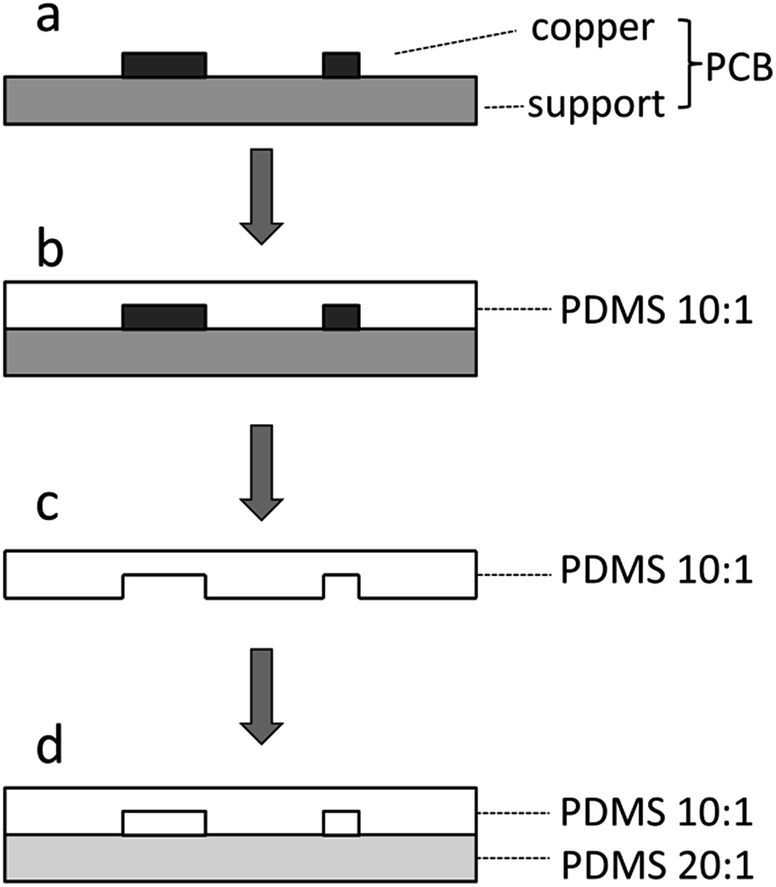 | ||
| Fig. 1 A schematic of the device fabrication. (a) Using a commoditized PCB product as the master. (b) Pouring degassed PDMS prepolymer (10:1 silicone elastomer with curing agent) over the PCB master. (c) Peeling off the semi-cured PDMS replica from the master. (d) Bonding the channel layer to a flat layer, which was fabricated using 20:1 silicone elastomer with the curing agent. | ||
Imaging
The cured PDMS microfluidic devices were cut into cross sections using a blade. An optical inverted microscope (IX81, Olympus Corporation, Tokyo, Japan) equipped with a CCD camera (Model GO-3-CLR-10, QImaging Corporation, Surrey, BC, Canada) was used to obtain the images of the cross-sections. The flow and droplet behaviors were observed using the same optical system.The surface morphology of the PCB masters and PDMS replicas was observed using field emission scanning electron microscopy (Model Ultra Plus, Carl Zeiss Microscopy GmbH, Oberkochen, Germany).
Characterization of bonding
An extremely high flow rate, 10 μL s−1, was employed to pump distilled water into the fabricated devices to characterize the effect of bonding. The devices used were fabricated by molding the PCB master, as shown in Fig. 2. The copper foils are 10 mil (about 254 μm) wide in the channel. Edible pigments (DAB Baking Corporation, Shanghai, China) were used to enhance the visual effects. We also tried to tear the fabricated PDMS-based devices along the bonded surfaces.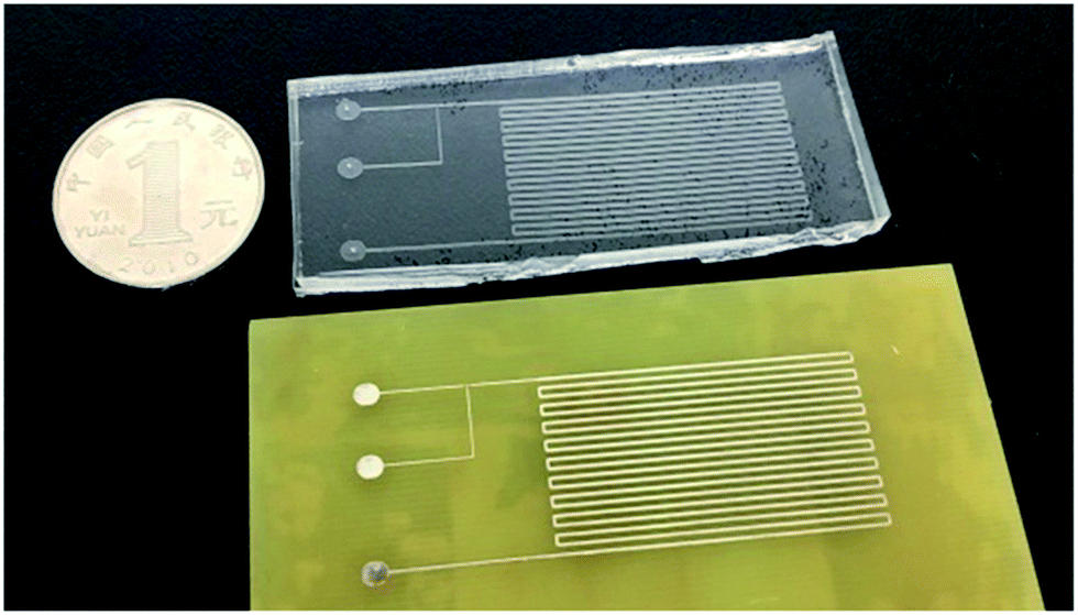 | ||
| Fig. 2 An example of the commoditized PCB and the cured PDMS replica. | ||
Droplet generation
For generating emulsions, 90 μL of Span80 (Sigma Chemical Corporation, St. Louis, MO, USA), 8 μL of Tween80 (Sigma) and 1 μL of Triton X-100 (Sigma) were pipetted into 1901 μL of mineral oil (Sigma) to prepare the oil phase. Once the reagents were combined, the tube was capped and vortexed until all of supplements were incorporated into the mineral oil. A water phase was prepared using distilled water. Edible pigments (DAB Baking Corporation, Shanghai, China) were used to enhance the visual effects. In the PCB masters of the T-junction drop generator, the copper foils are 20 mil (about 508 μm) wide in the channel, tapering to 10 mil (about 254 μm) wide in the region where water and oil meet at the cross-flow intersection. In the PCB masters of the flow focusing drop generator, the copper foils are also 20 mil (about 508 μm) wide in the channel, tapering to 10 mil (about 258 μm) wide at the cross-flow intersection. In the two types of drop generators, the oil phase was pumped using a syringe pump (L0107-2A, LongerPump, Baoding, China) at 50 μL h−1, and the water phase was pumped at 10 μL h−1.Matlab (Mathworks Corporation, Natick, MA, USA) was used for image processing and calculating the equivalent diameter. Our image processing pipeline referenced the published protocol.26 Briefly, the original images were binarized to extract the outline of the droplets. After that, the area within the outline was blackened and the number of black pixels was counted to calculate the cross-sectional area of the droplets. The equivalent diameter of a droplet was calculated based on assuming the cross-section of the droplets to be a standard circle. To evaluate the stability of the drop generators, the distance between the centers of two adjacent droplets was calculated and considered to be the spacing of the droplets.
Droplet operations
A symmetrical T-junction structure and asymmetric T-junction structure were fabricated for droplet break-up. The copper foils in the masters of the symmetrical T-junction are 6 mil (about 152 μm) wide. In the master of the asymmetric T-junction, the copper foil of the input channel is 10 mil (about 254 μm) wide, the copper foil of the wide output channel is 15 mil (about 381 μm) wide and the copper foil of the narrow output channel is 6 mil (about 1502 μm) wide. The droplets were generated upstream by the T-junction drop generators. The oil phase was pumped using a syringe pump (L0107-2A, LongerPump, Baoding, China) at 100 μL h−1 and the water phase was pumped at 40 μL h−1. Matlab (Mathworks Corporation, Natick, MA, USA) was used for image processing and calculating the equivalent diameter of the daughter droplets formed in the symmetrical T-junction according the pipeline mentioned above.A symmetrical coalescence chamber was fabricated for droplet fusion. In the PCB master, the main channel is 10 mil (about 254 μm) wide, tapering to 20 mil (about 508 μm) in the symmetrical coalescence chamber where the droplets fuse. The droplets are generated upstream by a flow focusing drop generator. The oil phase was pumped by a syringe pump (L0107-2A, LongerPump, Baoding, China) at 100 μL h−1, and the water phase was pumped at 20 μL h−1.
An additional T-junction was designed for droplet loading. In the PCB masters, the input and output channel are 10 mil (about 254 μm) wide, and the loading channel tapers to 8 mil (about 203 μm) wide in the region where the droplets and loading water meet at the cross-flow intersection. The droplets were generated upstream by another T-junction drop generator. The oil phase was pumped by a syringe pump (L0107-2A, LongerPump, Baoding, China) at 100 μL h−1, the water phase containing red edible pigment for droplet generation was pumped at 30 μL h−1 and the loading water containing green edible pigment was pumped at 10 μL h−1.
Droplet sorting by multi-height structures
Multi-height structures for passive droplet sorting were fabricated according to a literature procedure.27 Briefly, two PCB masters were prepared to construct the multi-height device. The first PCB master contained a 70 mil (about 1778 μm) wide channel. The second PCB master contained two parallel bulges, which molded the two parallel grooves (channels) in the PDMS replicas. The main groove in which the droplets are formed upstream is 8 mil (about 152 μm) wide, and the groove parallel to the main groove is 10 mil (about 254 μm) wide. The PDMS replicas of the first PCB master and the second PCB master were then tightly pressed and bonded (Fig. S1†).In a channel with a parallel groove structure on the main route, a main flow exists in the channel direction and a side flow exists in the parallel groove direction.27 The side flow produces a driving force on the droplets in the main route. If the size or deformation of a droplet is large enough to be partially located on the new groove, the droplet experiences Laplace pressure in the new groove. In some new grooves, the Laplace pressure is lower than that in the old grooves. In this condition, the droplets can move from the old groove to the new groove.
Results and discussion
Generation of PDMS replicas on commoditized PCB masters
The designed PCB documents, which contained the microstructure patterns, were sent to a common PCB manufactory and fabricated. The microfluidic devices can be easily fabricated using the commoditized PCB masters. The procedure used to prepare the PDMS-based devices is illustrated in Fig. 1 and involves pouring over a 10:1 PDMS mixture on the commoditized PCB master to form a negative replica, peeling off the replica from the master, preparing a flat PDMS replica or another replica with negative relief pattern using a 20:1 mixture and sealing the two PDMS replicas to form the complete microfluidic devices. The pattern of the microchannels on the commoditized PCB master was manifolded in the PDMS replica (Fig. 2). The SEM images of the PCB master strengthen the evidence16,19 that the surface of the supportive material in the PCB is quite rough (Fig. 3a). Craters were observed all over the surface of the supportive material. The surface of the PDMS replicas is also rough (Fig. 3b), and the difference is that the negative relief patterns of the craters are all over the surface. PDMS replicas with such rough surfaces are difficult to seal against glass slides even with the assistance of plasma treatment. Therefore, commoditized PCB masters were not previously used to fabricate PDMS replicas. A modified PCB manufacture procedure was applied or thermoplastic elastomers were used to overcome this difficulty. The cross-section of a microchannel in the fabricated PDMS device exhibits a characteristic trapezoidal sidewall profile (Fig. 3c). It was yielded by the isotropic nature of the copper etching process of the PCB masters, which has been previously reported.16,24 The relatively large scale in microstructure and the isotropic nature restrict PCB masters to be used in molding replicas with precise structures. However, the precision degree of PCB masters reaches the requirements of a lot of microfluidic applications, such as cell-based assays,28–31 droplet formation and operations,22,32 microbead based analyses33 and the generation of concentration gradients.23
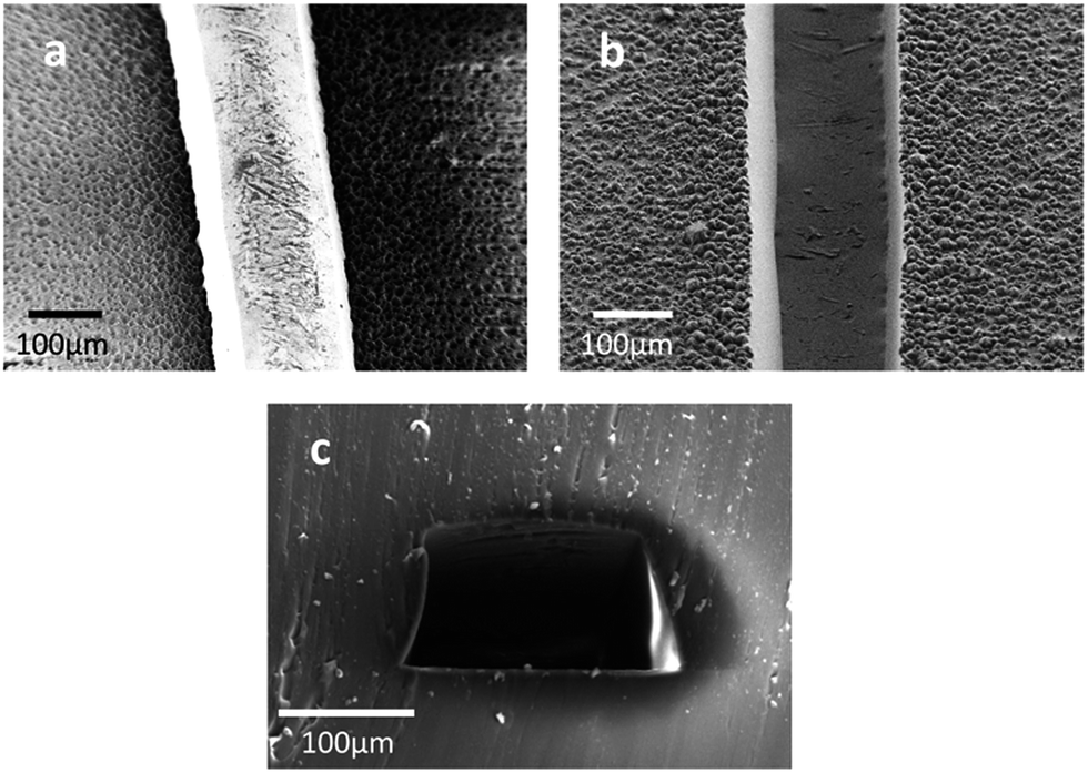 | ||
| Fig. 3 The SEM images of the PCB master (a), cured PDMS replica (b) and the cross-section of a channel in the fabricated PDMS device (c). | ||
In this study, the insufficient adhesion due to the surface roughness was solved by sealing two semi-cured PDMS replicas. The techniques of bonding two layers of semi-cured silicone together have been established for about 15 years34 and are widely used. The PDMS prepolymer and curing agent were mixed at different ratios for the two replicas. The excess curing agent in one replica promotes cross-linking with the excess silicone in the other replica. Pioneers had fabricated two PDMS-based devices using a similar procedure.21 However, whether the bonding was firm and the fabricated devices were practical is unclear due to the lack of in-depth exploration and applications. Herein, we characterized the effect of bonding by pumping distilled water into the fabricated devices at an extremely high flow rate, 10 μL s−1. No leakage was observed in the fabricated devices (Video S1†). Furthermore, in the tearing experiments, the fabricated devices cracked within one PDMS layer, instead of splitting along the bonding surfaces (Fig. S2†). These results demonstrated that a firm and irreversible bond was formed between the two semi-cured PDMS replicas.
Directly using the commoditized PCB masters avoids fabricating ordinary PCBs or modified PCBs in the laboratory. The procedure for fabricating PCBs is not complicated, but involves the printing of photomasks, exposure of the photoresist by UV irradiation, removal of the developed photoresist and the etching of the unprotected copper layer.19 Moreover, to fabricate replicas with a smooth surface, the etching conditions require specialized optimization for the partial removal of the copper layer.28 A lot of equipment and chemical reagents are required for the fabrication, including high-resolution printers, UV lamps, photoresistors, PCB developer powder, etching reagent containing FeCl3, acetone and metal polishing reagents. In contrast, almost no equipment was required in entire procedure presented in this study, except a vacuum pump and an oven. These two devices are commonly equipped in all types of laboratories. Thermoplastic elastomers, such as SEBS, are melt processable materials and are typically much easier to bond. The rough thermoplastic elastomer replicas can be solidly sealed against glass or an elastomer by heating the material to a temperature just below its softening point.20 Strong uniform bonds are easily achieved with glass or elastomer surfaces. In a previous study, polyethylene terephthalate substrates and the PDMS replicas, which were molded using the PCB masters, were bonded to form a microfluidic sensing platform.35 Each bonding surface was treated using corona discharge treatment before pressed together overnight. The experiments were well performed on the sealed devices, but a laboratory corona apparatus was needed to be used. Although thermoplastic elastomers and polyethylene terephthalate have some manufacturing advantages for flexible microfluidic systems, the thermosetting PDMS is more widely accepted and is the polymer of choice for rapidly prototyping polymer microfluidics.25 For the laboratories of different fields, PDMS is more familiar and practical than thermoplastic elastomers. The convenient procedure, minimal requirement of equipment and use of the general polymer PDMS will make this method well accepted and widely applied.
Fabricated PDMS-based microfluidic devices for droplet generation
Droplets can be generated by specific microstructures, such as the T-junction structure6 and flow focusing structure.36,37 We have explored the feasibility and stability of droplet formation by the PDMS-based microfluidic devices using commoditized PCBs as the masters. A T-junction drop generator and flow focusing drop generator were both fabricated and investigated. Droplets were successfully generated in the two types of droplet generators (Fig. 4a and d). The mean area of each droplet was measured, the equivalent diameter was calculated by considering the droplets as standard circles and the histograms of the dropsize distribution were obtained (Fig. 4b and e). The polydispersity (the coefficient of variation of the drop equivalent diameter) was found to be 0.91% over a population of 50 drops using the T-junction drop generator and 0.87% using the flow focusing drop generator. Using the majority of microfluidic methods, the polydispersity of the produced droplets can be as low as 1–3%.38,39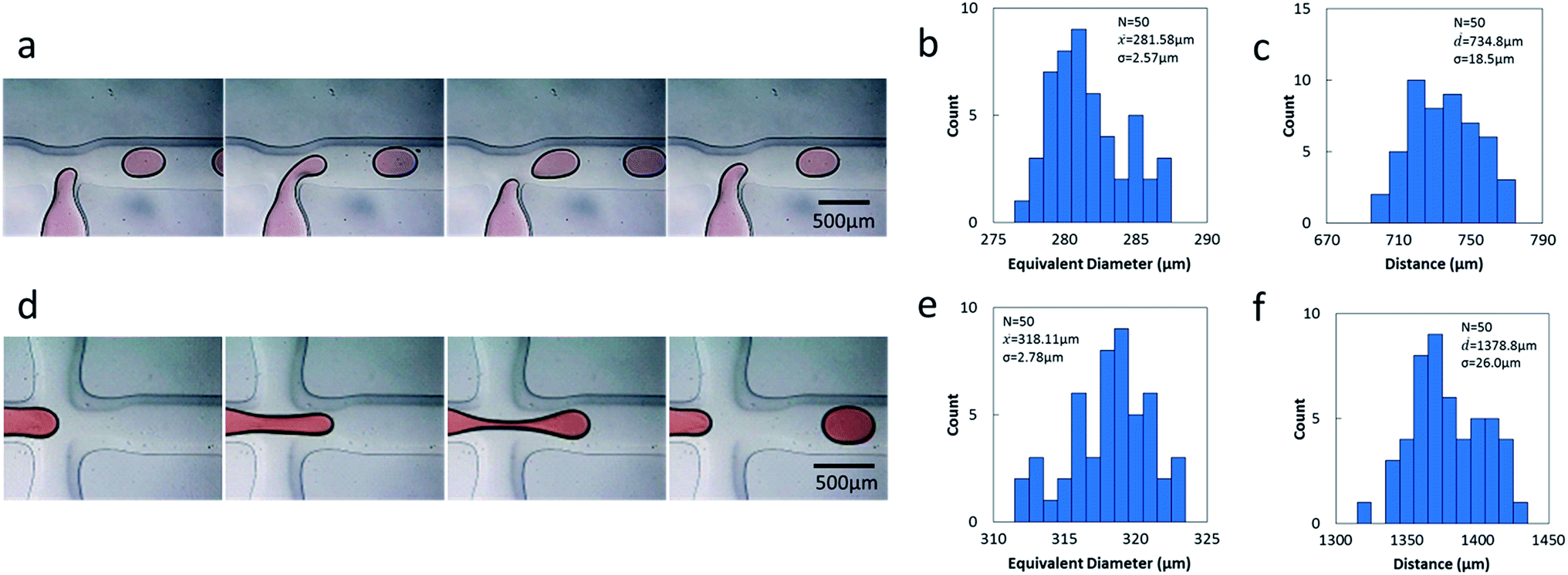 | ||
| Fig. 4 Analysis of the two drop generators. (a) Droplet formation in a T-junction drop generator. (b) Histogram of the droplet size distribution. The droplets were generated by the T junction device. (c) Histogram of the droplet distance distribution. The distances between the adjacent droplets generated by the T-junction device were measured. (d) Droplet formation in a flow focusing drop generator. (e) Histogram of droplet size distribution. The droplets were generated by the flow focusing device. (f) Histogram of distance distribution. The distances between the adjacent droplets generated by the flow focusing device were measured. | ||
The droplets produced by the two generators are comparable with the droplets produced by the majority of droplet generators used in polydispersity studies. The stability of the drop generators was evaluated by exploring the distance distribution between the droplets (Fig. 4c and f). The coefficient of variation for the distance between the adjacent droplets is 2.51% using the T-junction drop generator and 1.88% using the flow focusing drop generator. The excellent monodispersity and stable distance between the droplets demonstrates that the method described here is reliable, and the fabricated devices are useful in droplet formation.
Droplet operations in the PDMS-based microfluidic devices
Drop splitting, merging, loading and sorting are essential operations in droplet microfluidics. To further demonstrate the reliability of the fabricated PDMS-based devices, these essential operations were all performed in the devices molded against commoditized PCB masters. For drop splitting, a symmetric T-junction structure and asymmetric T-junction structure were fabricated according to the published designation.7 As anticipated, the droplets generated upstream always broke into two daughter droplets of approximately equal sizes in the symmetrical T-junction (Fig. 5a). The difference of equivalent diameters between the right and the left daughter droplets is smaller than 10% (Fig. S3†). In contrast, the droplets broke asymmetrically in the T-junction with relative sidearm widths of 2.5 (wide sidearm 15 mil, narrow sidearm 6 mil) (Fig. 5b). For drop merging, a symmetrical coalescence chamber was fabricated according to a literature procedure.8 The droplet pairs were destabilized while passing through the chamber, from separated to collided, and finally fused (Fig. 5c). In drop loading, an additional T-junction was designed and fabricated. The droplets containing red edible pigment met the loading water containing green edible pigment at the cross-flow intersection and were dipped in the green loading water (Fig. 5d).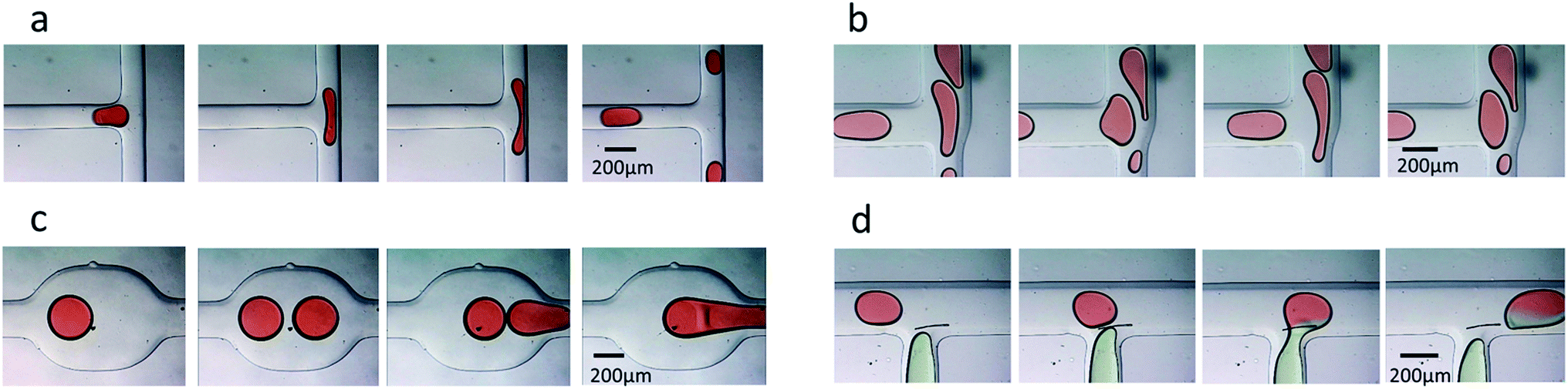 | ||
| Fig. 5 The time sequence showing the droplet operations in the PDMS devices using commercial PCBs as the masters and bonding without using plasma. (a) The passive breakup at a symmetric T-junction. (b) The passive break-up at the asymmetric T-junction. (c) Fusion at an symmetric coalescence chamber. (d) Loading at the T-junction. | ||
To demonstrate the feasibility of fabricating multi-height microfluidic devices using PCB masters, a passive droplet sorting structure with two parallel grooves was molded according to a literature procedure.27 Two molded replicas with negative relief patterns were bonded together to fabricate structures of two heights in one device. The side flow existing in the parallel groove direction produced a driving force on droplets in the main route. In the fabricated multi-height device, droplets of large size deformed and were partially located on the new groove. The lower Laplace pressure in the new groove drove the large droplets away from the old groove and moved to the new groove (Fig. 6a). The droplets of small size were not large enough to be partially located on the new groove and stayed in the main route (Fig. 6b). Droplets of different sizes were sorted using this PDMS-based device (Fig. 6c). The results supported that multi-height devices can be reliably constructed using two PDMS replicas, which are molded against commoditized PCBs.
 | ||
| Fig. 6 The different droplet routes and deformation behavior in the rail channel. (a) A large droplet transfers to a new rail. (b) A small droplet stays in the old rail. (c) Droplets of different sizes, routes and deformation behavior in the rail channel. | ||
All of the essential operations in droplet microfluidics were reliably conducted using these PDMS-based microfluidic devices, even the operations requiring multi-height devices. The results demonstrated that the methods described in this study are reliable and practical in droplet microfluidics.
Conclusions
In conclusion, we have developed a convenient method for fabricating PDMS-based microfluidic devices directly using commoditized PCBs as the masters. The PCB masters were fabricated using a common PCB manufactory with standard industrial etching techniques. Additional curing of two semi-cured PDMS replicas accomplished efficient bonding and avoided insufficient adhesion due to the rough surfaces of PDMS replicas. The widely accepted polymer, PDMS, is familiar and practical to most researchers in different fields. Only two commonly used equipments are required in device fabrication. Highly monodisperse droplets with polydispersity values smaller than 1% were stably formed and delicately operated using the easily fabricated PDMS-based devices. Moreover, the droplets were orderly sorted by the microstructures in the fabricated multi-height devices. Due to the ease of fabrication, minimal requirement of equipment and use of the general polymer PDMS, the methods described in this study should be popular microfabrication tools for researchers who intend to carry out studies with preliminarily microfluidics devices.Acknowledgements
This study was supported by the National Key Project of China (No. 2016YFA0501600), project 61571121 of the National Natural Science Foundation of China and the Fundamental Research Funds for the Central Universities of China.References
- W. Q. Yue, C. W. Li, T. Xu and M. S. Yang, Biosens. Bioelectron., 2013, 41, 675–683 CrossRef CAS PubMed.
- J. de Jong, R. G. H. Lammertink and M. Wessling, Lab Chip, 2006, 6, 1125–1139 RSC.
- P. N. Floriano, N. Christodoulides, D. Romanovicz, B. Bernard, G. W. Simmons, M. Cavell and J. T. McDevitt, Biosens. Bioelectron., 2005, 20, 2079–2088 CrossRef CAS PubMed.
- J. E. Kim, J. H. Cho and S. H. Paek, Anal. Chem., 2005, 77, 7901–7907 CrossRef CAS PubMed.
- Y. Marcy, T. Ishoey, R. S. Lasken, T. B. Stockwell, B. P. Walenz, A. L. Halpern, K. Y. Beeson, S. M. D. Goldberg and S. R. Quake, PLoS Genet., 2007, 3, 1702–1708 CAS.
- T. Thorsen, R. W. Roberts, F. H. Arnold and S. R. Quake, Phys. Rev. Lett., 2001, 86, 4163–4166 CrossRef CAS PubMed.
- D. R. Link, S. L. Anna, D. A. Weitz and H. A. Stone, Phys. Rev. Lett., 2004, 92, 054503 CrossRef CAS PubMed.
- N. Bremond, A. R. Thiam and J. Bibette, Phys. Rev. Lett., 2008, 100, 024501 CrossRef PubMed.
- S. Ostrovidov, J. L. Jiang, Y. Sakai and T. Fujii, Biomed. Microdevices, 2004, 6, 279–287 CrossRef CAS PubMed.
- H. C. Fan, J. B. Wang, A. Potanina and S. R. Quake, Nat. Biotechnol., 2011, 29, 51–57 CrossRef CAS PubMed.
- A. Manz, J. C. Fettinger, E. Verpoorte, H. Ludi, H. M. Widmer and D. J. Harrison, TrAC, Trends Anal. Chem., 1991, 10, 144–149 CrossRef CAS.
- D. Qin, Y. N. Xia and G. M. Whitesides, Adv. Mater., 1996, 8, 917–919 CrossRef CAS.
- D. C. Duffy, J. C. McDonald, O. J. A. Schueller and G. M. Whitesides, Anal. Chem., 1998, 70, 4974–4984 CrossRef CAS PubMed.
- Y. N. Xia and G. M. Whitesides, Annu. Rev. Mater. Sci., 1998, 28, 153–184 CrossRef CAS.
- C. Khoury, G. A. Mensing and D. J. Beebe, Lab Chip, 2002, 2, 50–55 RSC.
- M. Abdelgawad, M. W. L. Watson, E. W. K. Young, J. M. Mudrik, M. D. Ungrin and A. R. Wheeler, Lab Chip, 2008, 8, 1379–1385 RSC.
- T. Merkel, M. Graeber and L. Pagel, Sens. Actuators, A, 1999, 77, 98–105 CrossRef CAS.
- A. Wego, S. Richter and L. Pagel, J. Micromech. Microeng., 2001, 11, 528–531 CrossRef CAS.
- C. W. Li, C. N. Cheung, J. Yang, C. H. Tzang and M. S. Yang, Analyst, 2003, 128, 1137–1142 RSC.
- A. P. Sudarsan, J. Wang and V. M. Ugaz, Anal. Chem., 2005, 77, 5167–5173 CrossRef CAS PubMed.
- A. P. Sudarsan and V. M. Ugaz, Anal. Chem., 2004, 76, 3229–3235 CrossRef CAS PubMed.
- W. Q. Yue, C. W. Li, T. Xu and M. S. Yang, Lab Chip, 2011, 11, 3352–3355 RSC.
- C. W. Li, R. S. Chen and M. S. Yang, Lab Chip, 2007, 7, 1371–1373 RSC.
- J. Y. Jiang, J. S. Zhan, W. Q. Yue, M. S. Yang, C. Q. Yi and C. W. Li, RSC Adv., 2015, 5, 36036–36043 RSC.
- D. Sameoto and A. Wasay, Proc. SPIE, 2015, 9320, 932001 CrossRef.
- A. S. Basu, Lab Chip, 2013, 13, 1892–1901 RSC.
- D. H. Yoon, S. Numakunai, A. Nakahara, T. Sekiguchi and S. Shoji, RSC Adv., 2014, 4, 37721–37725 RSC.
- C. W. Li, J. Yang and M. S. Yang, Lab Chip, 2006, 6, 921–929 RSC.
- L. Zhao, P. Cheng, J. X. Li, Y. Zhang, M. M. Gu, J. Liu, J. R. Zhang and J. J. Zhu, Anal. Chem., 2009, 81, 7075–7080 CrossRef CAS PubMed.
- J. Yang, J. Yang, Z. Q. Yin, I. Svir, J. Xu, H. Y. Luo, M. Wang, Y. Cao, N. Hu, Y. J. Liao and X. L. Zheng, Anal. Chim. Acta, 2009, 634, 61–67 CrossRef CAS PubMed.
- H. Zou, W. Q. Yue, W. K. Yu, D. D. Liu, C. C. Fong, J. L. Zhao and M. S. Yang, Anal. Chem., 2015, 87, 7098–7108 CrossRef CAS PubMed.
- A. P. Sudarsan and V. M. Ugaz, Lab Chip, 2006, 6, 74–82 RSC.
- W. Q. Yue, H. Zou, Q. H. Jin, C. W. Li, T. Xu, H. Y. Fu, L. C. H. Tzang, H. Y. Sun, J. L. Zhao and M. S. Yang, Biosens. Bioelectron., 2014, 54, 297–305 CrossRef CAS PubMed.
- T. Thorsen, S. J. Maerkl and S. R. Quake, Science, 2002, 298, 580–584 CrossRef CAS PubMed.
- B. B. Narakathu, S. G. R. Avuthu, A. Eshkeiti, S. Emamian and M. Z. Atashbar, IEEE Sens. J., 2015, 15, 6374–6380 CrossRef CAS.
- S. L. Anna, N. Bontoux and H. A. Stone, Appl. Phys. Lett., 2003, 82, 364–366 CrossRef CAS.
- R. Dreyfus, P. Tabeling and H. Willaime, Phys. Rev. Lett., 2003, 90, 144505 CrossRef PubMed.
- G. F. Christopher and S. L. Anna, J. Phys. D: Appl. Phys., 2007, 40, R319–R336 CrossRef CAS.
- C. T. Chen and G. B. Lee, J. Microelectromech. Syst., 2006, 15, 1492–1498 CrossRef.
Footnote |
| † Electronic supplementary information (ESI) available: Schematic diagram for multi-height device fabricating. Tearing experiments of the sealed PDMS-based microfluidic devices. Histogram of daughter droplet size distribution. See DOI: 10.1039/c7ra03899b |
| This journal is © The Royal Society of Chemistry 2017 |