 Open Access Article
Steering photoinduced charge kinetics via anionic group doping in Bi2MoO6 for efficient photocatalytic removal of water organic pollutants†
Yongxing Xing,
Jing Zhang,
Zhiliang Liu and
Chunfang Du
 *
*
College of Chemistry and Chemical Engineering, Inner Mongolia University, Hohhot, Inner Mongolia 010021, P. R. China. E-mail: cedchf@imu.edu.cn; Fax: +86-471-4994375; Tel: +86-471-4994375
First published on 19th July 2017
Abstract
In this work, we report a novel anionic group doped Bi2MoO6 with noble metal loading as an excellent photocatalytic material for the efficient photodegradation of organic pollutants, including rhodamine B (RhB) and colorless o-phenylphenol (OPP). Several characterization techniques were conducted to investigate the effect of anionic group doping and noble metal loading on the lattice structure, electronic structure, defect chemistry as well as photocatalytic performance. It's found that CO32− doping in a Bi2MoO6 host matrix led to lattice expansion, local symmetry distortion, oxygen vacancy generation and band gap narrowing from ∼2.60 to ∼2.31 eV. VB-XPS, Mott–Schottky plots and DFT results indicated that the variation of the band gap energy for Bi2MoO6 mainly originated from the upward shift of the valence band edge, which is attributed to the presence of the midgap states of the C 1s orbital. Noble metals (Au, Ag and Pd) as cocatalysts forcefully improved the photogenerated charge separation. With contributions from the doping effects and cocatalysts, the photocatalytic activity of 0.5% Pd–3C/BMO was robustly enhanced about 5-fold for RhB degradation within 40 min under UV + visible light irradiation and 29-fold for OPP degradation within 120 min under visible light irradiation in comparison with pristine Bi2MoO6, respectively.
1. Introduction
Photocatalytic decomposition or mineralization of organic pollutants such as phenol, p-chlorephenol and o-phenylphenol with high degradation rates and low toxicity has been recognized as a promising strategy in environmental remediation since these organic pollutants are difficult to eliminate using conventional water treatment process.1–4 Photocatalysis with naturally abundant solar light is a perfect development direction that need all mankind to make efforts to try. In such a way, photocatalysts are required to respond in a broad wavelength range. Element doping and noble metal loading are two efficient approaches to enhance the visible-light harvest and thus improve the photocatalytic performance of photocatalysts under visible-light irradiation.5,6Element doping is a fundamental strategy to introduce a small amount of atoms into the host crystal lattice, resulting in the modification of electronic dynamics and phonon transport or even regulation of the band gap and work function, both of which are beneficial for improving the photocatalytic activity.7–10 Most of the element-doping researches are concerned about metal or non-metal ions, such as Er3+/Fe3+ co-doped porous Bi5O7I,11 Mo doped Bi2WO6,7 B doped Bi2WO6,12 N–F co-doped BiVO4,13 etc. In comparison with cationic or anionic ions, anionic groups constituted by various elements and compositions possibly make more contributions to the regulation and management on the crystal lattice, optical harvest and photocatalytic performance.14–17 Self-doping of the CO32− anionic group into Bi2O2CO3 could induce a larger lattice spacing, extend the photoresponsive range from UV to visible light and the band gap could be also continuously tuned.14 PO4-doped Bi2WO6 synthesized by a urea-precipitation way showed the higher photocatalytic activity than that of pristine Bi2WO6 for the degradation of Cr(VI), RhB dye, phenol and antibiotics, etc.17 These excellent results imply that anionic group doping, a new concept, is a potential way to dramatically enhance the photocatalytic performance and makes the photocatalysts more practical for environmental requirement.15,16
Bismuth molybdate (Bi2MoO6), a member of the Aurivillius oxide family, has attracted considerable attention due to its unique physicochemical properties relating to its layered structure consisting of perovskite layers and bismuth oxide layers.18,19 However, the high recombination of photogenerated carriers and low utilization of solar energy inhibit its practical application.10,20 Until now, various strategies have been explored to solve these problems, including element doping even self-doping,21–25 heterojunction,26–30 noble metal loading,31–34 etc. However, anionic group doping has not been tried. Thus, in this paper, the anionic group CO32− was doped into the MoO6 sites in the host lattice of Bi2MoO6 to modulate the crystal and band-gap structures and extend the photoresponsive range for the first time. Then noble metals (Au, Ag and Pd) were loaded on Bi2MoO6 surfaces as the cocatalysts to further improve the photocatalytic activity. DFT calculation and series of characterization techniques were conducted to study the crystal structure, electronic band structure and optical properties. The photocatalytic performance was evaluated by the degradation of rhodamine B (RhB) and colorless o-phenylphenol (OPP) under UV + visible light or visible light irradiation. The mechanism of enhanced photocatalytic activity was also investigated. This work could possibly provide a new strategy for regulation and management of the crystal and band gap structures and thus enhance the photocatalytic performance of photocatalysts.
2. Experimental
2.1 Sample synthesis
2.2 Characterization
The phase structure of the synthesized samples was obtained on an X-ray diffractometer (EmpyreanPanalytical) with Cu Kα radiation (λ = 0.15406 nm). The detailed morphology and structure were recorded by transmission electron microscopy (TEM) and high resolution TEM (HRTEM) on a JEM-2010 apparatus with an acceleration voltage of 200 kV. Scanning electron microscopy (SEM) images were recorded on the Hitachi S-4800 apparatus with an accelerating voltage of 15 kV. The thermogravimetric analysis (TG) was conducted on a thermal analyzer (NETZSCH STA 449F3) when the sample was heated from 30 to 900 °C with a raising ramp rate of 10 °C min−1 under nitrogen atmosphere. X-ray photoelectron spectroscopy (XPS) was performed on a Thermo Escalab 250Xi with a monochromatic Al Kα (hν = 1486.6 eV) to determine the surface state and chemical composition. Raman spectra were recorded on a Horiba JobinYvonLabRAM HR800 instrument with the laser excitation of 320 nm. Fourier transform infrared spectroscopy (FT-IR) was carried out using a Bruker Tensor 27 spectrophotometer using KBr powder-pressed pellets. The UV-vis absorption spectra were measured using a UV-vis spectrophotometer (Lambda 750s) in the range of 200–800 nm. The specific surface area (SBET) of the samples was obtained from N2 adsorption–desorption isotherms at 77 K (ASAP 2020). The photoluminescence (PL) spectra were measured on an Edinburgh Instruments FLS920 spectrofluorimeter equipped with both continuous (450 W) and pulsed xenon lamps, with the excitation wavelength of 416 nm.The photocurrent transient response measurement, electrochemical impedance spectroscopy (EIS) and Mott–Schottky measurements were performed on a PGSTAT 302 N electrochemistry workstation. The measurement system contains a sample chamber, a lock-in amplifier (SR 830, Stanford Research Systems, Inc.) with a light chopper (SR540, Stanford Research Systems, Inc.) and a source of monochromatic light (500 W xenon lamp, CHF-XM 500, Trusttech) as well as a monochromator (Omni-λ 300, Zolix). The analyzed product is assembled as a sandwich-like structure of ITO–product–ITO, which ITO indicates an indium tin oxide electrode. All the measurements were performed in air atmosphere and at room temperature.
Oxygen vacancy and active species of hydroxyl (˙OH) and superoxide radicals (˙O2−) were detected by electron spin resonance (ESR) measurements on JEOL JES FA200 spectrometer. Oxygen vacancy measurement was conducted at 77 K. ESR spectra for hydroxyl radicals and superoxide radicals were conducted in methylbenzene solution (2.0 mL) and methylbenzene solution containing methyl alcohol (2 mL, the volume ratio of methyl alcohol being 20%), respectively. The experiments were performed in dark and under visible light irradiation with adding 4 mg sample and 0.05 mol L−1 DMPO (5,5′-dimethyl-1-pyrroline-N-oxide).
To investigate the crystal structure and electronic band structure of carbonate doped Bi2MoO6, density functional theory (DFT) calculation was performed using the CASTEP program package. The kinetic energy cutoff is 420 eV, using the generalized gradient approximation (GGA) with the Perdew–Burke–Ernzerhof (PBE) to treat the models. Geometry optimization is carried out until the residual forces were smaller than 0.01 eV Å−1, and the convergence threshold for self-consistent iteration was set at 5 × 10⁻⁷ eV.
2.3 Photocatalytic activity measurements
The photocatalytic activity was evaluated by degradation of water organic pollutants rhodamine B (RhB, 0.02 mol L−1) and colorless o-phenylphenol (OPP, 20 mg L−1) under various light irradiation. The photodegradation process was conducted in a photochemical reactor with different luminous power including 300 W and 500 W Xe lamp. Moreover, the photocatalytic performance was also investigated under UV + visible light irradiation (500 Xe lamp without cut-off filter) or visible light irradiation (500 W Xe lamp with a 420 nm cut-off filter), respectively.In every experiment, 30 mg of the prepared sample was suspended in 30 mL of RhB or OPP solution. Prior to irradiation, the suspension was kept in the dark with stirring for 60 min to reach adsorption–desorption equilibrium. During irradiation, 3 mL of suspension was sampled and centrifuged at certain time intervals. The absorbance of the as-obtained filtrates was measured at 552 nm and 282 nm using a UV-vis spectrophotometer (U-3900, Hitachi, Japan) to obtain the RhB and OPP concentrations, respectively. The normalized concentration change (C/C0) of the pollutant concentration was adopted to evaluate the photocatalytic performance, where C is the pollutant concentration at a certain time and C0 is the initiative concentration before illumination.
3. Results and discussion
3.1 Sample characterization
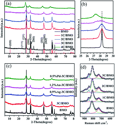
The XRD patterns of pristine Bi2MoO6 (BMO) and carbonate doped Bi2MoO6 (C/BMO) with various molar ratios of sodium citrate to Bi(NO3)3·5H2O are depicted in Fig. 1. All the diffraction peaks can be indexed to the orthorhombic Bi2MoO6 (JCPDS card no. 77-1246) when the molar ratio of sodium citrate to Bi(NO3)3·5H2O is below 4 (Fig. 1a). With an increase of the carbonate doping amount, the amplifying XRD pattern (Fig. 1b) displays that the peak (131) located at about 28.2° shows a slight shift toward smaller angles compared with pristine Bi2MoO6. According to Bragg's law (2d![[thin space (1/6-em)]](https://www.rsc.org/images/entities/char_2009.gif) sin
sin![[thin space (1/6-em)]](https://www.rsc.org/images/entities/char_2009.gif) θ = nλ), a smaller 2θ indicates a larger lattice spacing.7,10,14 By a least-squares method, the lattice parameters for carbonate doped Bi2MoO6 were given in Fig. S1.† As depicted in Fig. S1,† a monotonous increase in the lattice volume was observed with an increase of initial molar ratios of sodium citrate to Bi(NO3)3·5H2O, which may suggest that carbonate groups were incorporated in Bi2MoO6 host matrix. On the other hand, it is noted that the diffraction peaks in Fig. 1a greatly broadened with an increase of carbonate doping content. Using Scherrer formula, the average size of pristine Bi2MoO6 was calculated to be 52.9 nm from peaking broadening. For 3C/BMO sample, the average size was greatly reduced to 4.1 nm (Fig. S1†). Low grain size of 3C/BMO predicts large surface to volume ratios and more active sites that is benefit for enhancement of photocatalytic performance. When the molar ratio of sodium citrate to Bi(NO3)3·5H2O increases to 4, the crystal phase transforms to Bi2O3, thus the product 4C/BMO will not be referred in the following discussion.
θ = nλ), a smaller 2θ indicates a larger lattice spacing.7,10,14 By a least-squares method, the lattice parameters for carbonate doped Bi2MoO6 were given in Fig. S1.† As depicted in Fig. S1,† a monotonous increase in the lattice volume was observed with an increase of initial molar ratios of sodium citrate to Bi(NO3)3·5H2O, which may suggest that carbonate groups were incorporated in Bi2MoO6 host matrix. On the other hand, it is noted that the diffraction peaks in Fig. 1a greatly broadened with an increase of carbonate doping content. Using Scherrer formula, the average size of pristine Bi2MoO6 was calculated to be 52.9 nm from peaking broadening. For 3C/BMO sample, the average size was greatly reduced to 4.1 nm (Fig. S1†). Low grain size of 3C/BMO predicts large surface to volume ratios and more active sites that is benefit for enhancement of photocatalytic performance. When the molar ratio of sodium citrate to Bi(NO3)3·5H2O increases to 4, the crystal phase transforms to Bi2O3, thus the product 4C/BMO will not be referred in the following discussion.
As known that Raman scattering is regarded as an effective technique to check the lattice strain of semiconductor.14,35 Thus, to further understand the crystal defects and crystal structure distortion in carbonate doped Bi2MoO6 structures, Raman spectra were measured and displayed in Fig. 1d and S2.† As shown in Fig. S2† and enlarged spectra in Fig. 1d, all of the C/BMO samples exhibit the typical vibration mode of Bi2MoO6. The vibration modes near 292 cm−1 are assigned to the Eg bending vibrations, while the peaks located at 334 and 366 cm−1 are attributed to Eu symmetric bending.20,21 The Raman vibrations, while the peaks located at 334 and 366 cm−1 are attributed to Eu symmetric bending.20,21 As illustrated in Fig. 1d, the Raman signal in the range of 550–950 cm−1 can be well reproduced by three vibration peaks. The Raman vibrations at 732 cm−1 (Eu mode), 811 cm−1 (A1g mode), 857 cm−1 (A2u mode) are assigned to the asymmetric, symmetric and asymmetric stretching vibrations of the MoO6 octahedrons, respectively.36,37 Compared with those of pristine Bi2MoO6, the Raman peaks of carbonate dope Bi2MoO6, taking the intense peak at 811 cm−1 in Fig. 1d and 334 cm−1 in Fig. S2† as examples, shift slightly toward lower wavenumbers with increasing the carbonate doping content. In addition, the Mo–O bond length calculated by the empirical equation RMo–O = 0.48239![[thin space (1/6-em)]](https://www.rsc.org/images/entities/char_2009.gif) ln(32
ln(32![[thin space (1/6-em)]](https://www.rsc.org/images/entities/char_2009.gif) 895/ν) is usually adopted to evaluate the crystal distortion, where R is the metal–oxygen bond length in angstroms and ν is the Raman stretching frequency in wavenumbers.10,36 According to this equation, the RMo–O calculated based on the Raman mode at 811 cm−1 changed from 1.7862 Å for pristine Bi2MoO6 to 1.7886 Å for 3C/BMO. This result forcefully confirms the result that the carbonate has been doped into the lattice crystal structure of Bi2MoO6, interpreting the distinct distortion and symmetry breaking of the MoO6 octahedron, which result is in consistent with that of Ce doped Bi2MoO6.10
895/ν) is usually adopted to evaluate the crystal distortion, where R is the metal–oxygen bond length in angstroms and ν is the Raman stretching frequency in wavenumbers.10,36 According to this equation, the RMo–O calculated based on the Raman mode at 811 cm−1 changed from 1.7862 Å for pristine Bi2MoO6 to 1.7886 Å for 3C/BMO. This result forcefully confirms the result that the carbonate has been doped into the lattice crystal structure of Bi2MoO6, interpreting the distinct distortion and symmetry breaking of the MoO6 octahedron, which result is in consistent with that of Ce doped Bi2MoO6.10
Sodium citrate was adopted as carbonate source to dope into the crystal lattice of Bi2MoO6, which generally decomposes when accelerating the temperature. Thus, thermogravimetric (TG) curves are measured to prove the existence of carbonate (Fig. S3†). The TG results reveal that the total weight loss of Bi2MoO6 is 4.7%, which can be attributed to the removal of adsorbed water.21 In comparison with pristine Bi2MoO6, the total weight loss of carbonate doped Bi2MoO6 increases with raising the carbonate doping content. This result is in accordance with that of carbonate doped Bi2O2CO3,14 which confirms the existence of carbonate in Bi2MoO6.
Fig. S4† presents the FTIR spectra of various samples. For pristine Bi2MoO6, the bands located at 841 and 800 cm−1 are assigned to the asymmetric and symmetric stretching of MoO6 referring vibration of the apical oxygen atoms, respectively.38 The band at 728 cm−1 is specified as the asymmetric stretching vibration of equatorial oxygen atoms of MoO6 octahedrons, and the band at 570 cm−1 is attributed to the bending vibration of MoO6.5 The band located at 445 cm−1 corresponds to the Bi–O stretching vibration. The bands at 3438 and 1388 cm−1 are assigned to the stretching vibration and deformation vibration of O–H.39 It should be noted that the FTIR spectra of carbonate doped Bi2MoO6 resemble that of pristine Bi2MoO6. However, a new broad band at 1569 is observed after carbonate doping, which is assigned to the C![[double bond, length as m-dash]](https://www.rsc.org/images/entities/char_e001.gif) C bonds of sodium citrate.39,40 This phenomenon further confirms the presence of carbonate.
C bonds of sodium citrate.39,40 This phenomenon further confirms the presence of carbonate.
The XRD patterns of noble metals (Au, Ag, Pd) loaded on 3C/BMO samples are shown in Fig. 1c. As displayed in Fig. 1c, loading of noble metals on the surface of 3C/BMO has a negligible influence on the XRD patterns of 3C/BMO. No peaks assigned to metal or metal oxide are observed even the Pd loading content reaching 1.0 wt% (Fig. S5†), which could be attributed to its low content or high dispersion of metal nanoparticles.41–43
XPS technique is usually employed to investigate the chemical state and prove the effect of doping.44,45 The survey XPS spectra and high-resolution XPS spectra of various elements for pristine BMO, 3C/BMO, 0.5% Pd–3C/BMO are displayed in Fig. S6† and 2. Two strong peaks located at 159.6 eV and 164.6 eV in Fig. 2a are assigned to Bi 4f7/2 and Bi 4f5/2, respectively. Another two strong peaks at 232.5 eV and 235.6 eV in Fig. 2b are attributed to Mo 3d5/2 and Mo 3d3/2, respectively. It is found that the Bi 4f and Mo 3d peaks shift to the lower bonding energy region after carbonate doping, which result is consistent with those of Ce doped Bi2MoO6 and La, F co-doped Bi2MoO6.10,23 This phenomenon confirms the incorporation of carbonate into the crystal lattice structure of Bi2MoO6, which results in the change of chemical environment for Mo center in the [MoO6] octahedron.23 Fig. 2c shows the high-resolution XPS spectra of O 1s. For pristine Bi2MoO6, the spectra can be deconvoluted into two peaks at 530.0 and 531.3 eV, which are assigned to the crystal lattice oxygen and surface hydroxyl groups, respectively.46,47 After carbonate doping, a new peak located at 532.0 eV could be observed, which is possibly attribute to the oxygen vacancies.48,49 To confirm the existence of oxygen vacancies, the ESR spectra were measured. As can be seen in Fig. 2h, the 3C/BMO sample presents a strong signal peak at g = 2.002, which is regarded as the typical characteristic of surface oxygen vacancies.49,50 It is generally accepted that doping could induce the crystal defects. Thus, the existence of oxygen vacancies could further confirm the successful doping of carbonate into the crystal lattice of Bi2MoO6. The high-resolution XPS spectra of C 1s are displayed in Fig. 2d. The spectra of 3C/BMO can be deconvoluted into three peaks at 284.8, 286.4 and 288.2 eV. The former peak belongs to the adventitious carbon from the instrument.14 The latter two peaks are assigned to C–OH and C–OOH bond,51,52 respectively, which further confirms the presence of carbonate after doping. The absence of band at 283.1 eV excludes a Bi–C bond formation or carbon doping.53 The binding energies at 83.8 and 87.4 eV in Fig. 2e are attributed to Au 4f7/2 and Au 4f5/2, respectively, which are characteristic of metallic Au.18 Fig. 2f shows two obvious peaks located at 368.2 and 374.2 eV, assigning to Ag 3d5/2 and Ag 3d3/2, respectively. The span between the two peaks is 6.0 eV, indicating the presence of Ag0.33 For the high-resolution Pd 3d XPS spectra in Fig. 2g, the peaks located at 335.2 and 340.5 eV belong to Pd 3d5/2 and Pd 3d3/2, respectively, which is an evidence of metallic Pd.34 The quantitative elemental analysis was conducted from the XPS data, as shown in Table S1.† From XPS spectra, the surface Bi/Mo molar ratio was determined to be 2.15 for pristine BMO, which is smaller than that of 2.69 for 3C/BMO. The variation of Bi/Mo molar ratio suggested the incorporation of carbonate groups into Bi2MoO6 host matrix. For 3C/BMO, the Bi/C molar ratio was determined to be 2.34. Moreover, the loading content of Ag, Au, and Pd was also determined by XPS peaks.
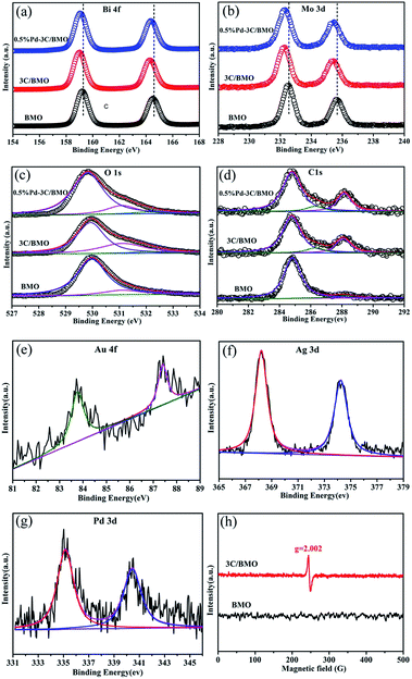 | ||
| Fig. 2 High-resolution XPS spectra of Bi (a), Mo (b), O (c), C (d), Au (e), Ag (f), Pd (g) and ESR spectra (h) at room temperature. | ||
The SEM images of pristine BMO, 3C/BMO and 0.5% Pd–3C/BMO are displayed in Fig. 3. The pristine BMO presents a sheet-like morphology with no more than 500 nm in width. In contrast to the morphology of pristine BMO, the morphology of 3C/BMO has no obvious changes except the reduced thickness and width, which result resembles that of Ce-doped Bi2MoO6.10 Moreover, the loading of noble metals on the surface of 3C/BMO also makes no effect on the morphology of 3C/BMO (Fig. 3c and S7†). To prove the presence of noble metals (taking Pd loaded sample as an example), the energy dispersive X-ray (EDX) analysis was employed and the results is shown in Fig. 3d. The result reveals that Bi, Mo, O, C and Pd are found and the corresponding element mapping images presented in Fig. 3e display the distribution of individual elements Bi, C and Pd in the 0.5% Pd–3C/BMO sample, confirming that Pd nanoparticles are uniformly dispersed in the 0.5% Pd–3C/BMO. From SEM analysis, it is seen an apparent particle size reduction, which is further confirmed by zeta potential measurement (Fig. S8†). From Fig. S8,† it is seen that the particle size distribution of BMO appeared at 50 nm, which is larger than that of 33 nm for 3C/BMO. Particle size reduction often accomplishes with increase of surface to volume ratios, which is of great importance to photocatalytic activity. Fig. S9† shows the N2 adsorption–desorption isotherms of pristine BMO, 3C/BMO and various noble metal loaded samples and the resultant specific surface areas and pore volumes are listed in Table S2.† After carbonate doping, the reduced thickness and width remarkably enhanced the specific surface area, which increases from 1.80 m2 g−1 to 40.8 m2 g−1 (nearly 22 times enhanced). The loading of Au, Ag and Pd also contributes to the specific surface area, which would be beneficial for the photocatalytic activity.
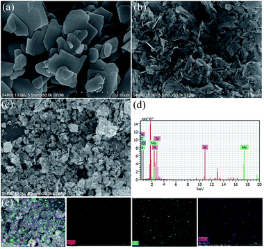 | ||
| Fig. 3 (a, b) SEM images of BMO and 3C/BMO, (c) SEM image, (d) EDX spectra and (e) STEM image and the corresponding element mapping of 0.5% Pd–3C/BMO. | ||
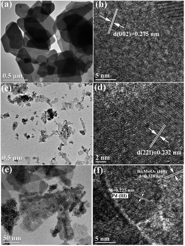
Fig. 4 displays the TEM and HRTEM images of pristine BMO, 3C/BMO and 0.5% Pd–3C/BMO. The TEM image of pristine BMO in Fig. 4a reveals the nanosheet-like morphology, which is consistent with the SEM result. The lattice fringes with the d spacing of 0.275 nm shown in Fig. 4b match well with the (002) crystalline plane of Bi2MoO6. In contrast to pristine Bi2MoO6, carbonate doping makes no obvious changes on the morphology of BMO but with reduced thickness and width for nanosheets (Fig. 4c). Fig. 4d shows that the lattice fringes with the d spacing of 0.232 nm correspond with the (221) crystalline plane of Bi2MoO6. Fig. 4e displays the TEM image of 0.5% Pd–3C/BMO. It can be clearly seen that Pd nanoparticles with an average diameter of 5–10 nm are uniformly dispersed on the surface of nanosheets. In HRTEM image of Fig. 4f, the lattice fringes with the d spacing of 0.328 nm are ascribed to the (140) crystalline plane of Bi2MoO6 and the lattice fringes with the d spacing of 0.225 nm match well with the (111) crystalline plane of Pd, which confirms the successful loading of Pd on the surface of Bi2MoO6. The TEM and HRTEM images as well as EDS data of 1.2% Au–3C/BMO and 0.9% Ag–3C/BMO are presented in Fig. S10.† The lattice fringes with the d spacing of 0.235 and 0.238 nm respectively belonged to the (111) crystalline plane of Au and (111) crystalline plane of Ag and EDS data also prove the existence of Au and Ag nanoparticles on the surface of Bi2MoO6. Moreover, the particle sizes of Ag and Au is close to that of Pd nanoparticle, which showed diameter of 5–10 nm.
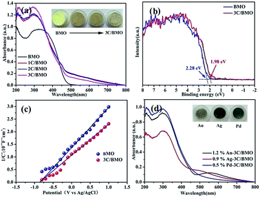
Associated with the photocatalytic activity is the electronic structure and band edge potentials of semiconductors that are highly dependent on the perturbation of lattice structure. As shown in Fig. 5a, either pristine BMO or CO32− doped BMO samples exhibited intense absorption band in the range of 200–500 nm, assigning to the typical electronic transition from O 2p/Bi 6s to Mo 4d orbitals, which is verified by the following DFT calculations. Interestingly, it is noted that a relatively weakened broad absorption ranging from 500 to about 800 nm is observed for all CO32− doped BMO samples. Inset of Fig. 5a displays the color changes of the as-prepared samples that varies from light-yellow to brown, providing indirect evidence of CO32− anionic group doping rather than carbon doping.14 Since Bi2MoO6 gives an indirect electronic transition feature,54 the band gap energy Eg can be estimated by the following equation: αhν = A(hν − Eg)1/2, where α, ν, A, and Eg are the absorption coefficient, incident light frequency, constant, and band gap energy, respectively. As a result, the band gap energies are determined to be ∼2.60 eV and ∼2.31 eV for pristine BMO and 3C/BMO, respectively. Apparently, a red shift of ∼0.29 eV for the band gap energy occurred after CO32− doping. Fig. 5b shows the VB-XPS spectra of BMO and 3C/BMO samples. The pristine BMO sample showed the edge of the maximum energy at about 2.28 eV, whereas the valence band edge of 3C/BMO shifted to 1.98 eV. This red shift value of the valence band edge is in accordance with that of the band gap energy narrowing, which gives an evidence that the variation of the band gap energy after CO32− doping mainly originates from the upward shift of the valence band edge. To further verify this presumption, Mott–Schottky measurement was used to investigate the conduction band positions of the as-prepared samples. Positive plots reveal an n-type character of both pristine BMO and 3C/BMO (Fig. 5c). The flat band potential of both pristine BMO and 3C/BMO is nearly identical, which is determined to be −0.85 V versus Ag/AgCl electrode, being equivalent to −0.63 V versus NHE. As well described in previous literatures,55 the conduction band of semiconductor is close to the flat band potential. The conduction band edge of both pristine BMO and 3C/BMO is estimated to be −0.63 V versus NHE, suggesting high redox potential for photocatalytic reactions. Moreover, the valence band edge of both pristine BMO and 3C/BMO can also be estimated to be 1.97 V and 1.68 V versus NHE, respectively. The Mott–Schottky result is greatly consistent with the VB-XPS observation. As for the enhanced absorption spectra among 500–800 nm for carbonate doped samples is possibly related to oxygen vacancies,48,56 which can be further confirmed by the following DFT calculations. Fig. 5d shows the UV-vis reflectance spectra of noble metals loaded on 3C/BMO samples. As shown in Fig. 5d, cocatalysts modification has minor impact on the absorption edge of 3C/BMO. For instance, the absorption feature of 0.5% Pd loaded 3C/BMO is close to that of 3C/BMO. However, for Ag and Au loaded samples, a weakened absorption band in the range of 500–700 nm appeared, which can be ascribed to the surface plasmon resonance of Ag and Au, respectively.
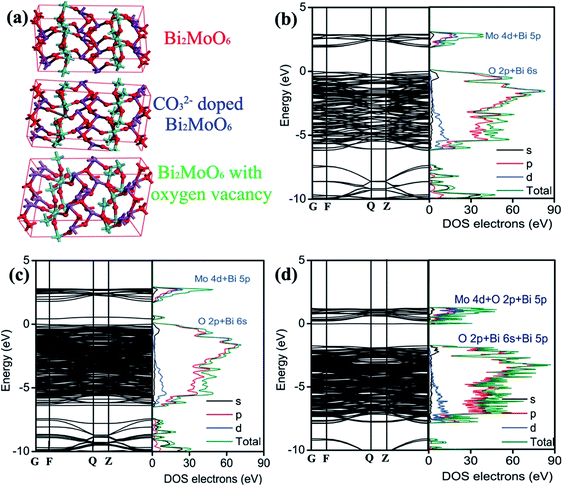
Having the above results in mind, it is therefore necessary to understand the doping effect of CO32− anionic group on the modification of the electronic structure and properties. The detailed knowledge of CO32− anionic group doping on the electronic structure modulation of Bi2MoO6 is obtained by calculating the band structure and partial density of states on the basis of DFT. On the grounds of the Bi2MoO6 unit cell, a supercell containing 72 atoms is employed for pure Bi2MoO6, as illustrated in Fig. 6a. Two different doping models based on this supercell are considered: one model is obtained by replacing one Mo with a C atom (denoted as C/Bi2MoO6). One defective model is obtained by deleting an oxygen near Mo site (denoted as VO/Bi2MoO6) because oxygen vacancy was detected in 3C/BMO sample (Fig. 2h) and meanwhile the doping of CO32− anionic group in Bi2MoO6 host matrix can produce oxygen vacancies due to the charge compensation effect. As shown in Fig. 6b, Bi2MoO6 shows an indirect optical transition character, which is in accordance with previous literature.54 The band gap energy for pure Bi2MoO6 is calculated to be 1.899 eV. The optical band edge is originated from the electronic transition between O 2p/Bi 6s and Mo 4d orbitals. From Fig. 6b, it is seen that the minimum conduction band of Bi2MoO6 mainly consists of the Mo 4d orbital and a minor hybridization of Bi 5p orbital in the energy region from 1.79 to 2.97 eV, as is illustrated in Fig. S11.† The maximum valence band consists of the hybridization of O 2p and Bi 6s orbitals in the energy region from 0 eV to −6.21 eV (Fig. S11†). With the model of C/Bi2MoO6, a new band contributed from the hybridization of O 2p and Bi 6s orbitals is observed, which is centered at about 0.52 eV (Fig. S12†). The appearance of a new electronic band can evidently result in the band gap narrowing of Bi2MoO6. The gap energy between the new band and Mo 4d orbital is determined to be 1.22 eV, which contracts about 35.8% in comparison to that of pure Bi2MoO6. However, the contraction of band gap energy of 3C/BMO with pristine BMO was calculated to be 11.2%, which is much smaller than the theoretical predication. On the other hand, the original electronic gap between O 2p/Bi 6s and Mo 4d orbitals is about 1.72 eV (Fig. 6c), which shows the contraction of about 9.43% in comparison with pure Bi2MoO6, being close to the experimental data. Therefore, the new electronic band probably contributes to the weakened absorption in the range of 500–800 nm. As for VO/Bi2MoO6 model (Fig. 6d), the minimum conduction band consists of the hybridization Mo 4d, O 2p and Bi 5p orbitals in the energy region from 0.20 eV to 1.18 eV (Fig. S13†). The maximum valence band consists of the hybridization of O 2p, Bi 6s and Bi 5p orbitals in the energy region from −1.75 eV to −7.89 eV (Fig. S13†). Moreover, a new electronic band was observed at −0.02 eV, which mainly consists of Bi 5s, Bi 5p orbitals and a little hybridization of Mo 4d orbital, being close to the conduction band minimum. The electronic gap was calculated to be about 1.73 eV between the electronic transition from O 2p, Bi 6s and Bi 5p orbitals to Bi 5s, Bi 5p and Mo 4d orbitals. Since both C/Bi2MoO6 and VO/Bi2MoO6 models predict new electronic bands, the band gap narrowing and weakened visible light absorption is thought to be related to CO32− doping and defect chemistry. Moreover, from Fig. 6d, it is clear that the construction of oxygen vacancy in Bi2MoO6 host matrix can narrow the band gap energy and meanwhile lead to the downward shift of the conduction band. However, on the basis of VB-XPS and Mott–Schottky results, an upward shift of the valence band is observed, which is contrary to the oxygen vacancy model. Therefore, the valence band edge shift may be mainly attributed to CO32− doping effects.
3.2 Photocatalytic test
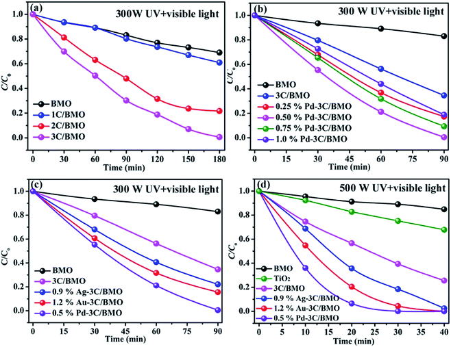
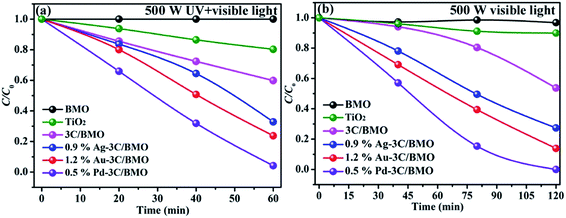
Organic dye RhB and colorless OPP are selected as the typical pollutants to evaluate the photocatalytic activity of as-prepared samples. Xe lamp with two kinds of luminous power including 300 W and 500 W are employed as the light source. Before irradiation, the suspension was placed in dark with continuously stirring to obtain adsorption–desorption equilibrium (Fig. S14†). The photocatalytic activities of various samples toward RhB with different luminous power are shown in Fig. 7. As shown in Fig. 7a, the pristine Bi2MoO6 showed poor photocatalytic activity toward RhB under UV + visible light irradiation with a luminous power of 300 W. With an increase of carbonate doping content, the photodegradation efficiency was heavily enhanced, which could reach nearly 100% within 180 min. Fig. 7b shows the photodegradation efficiency of 3C/BMO with various Pd loading content. The photocatalytic activity was further enhanced after Pd loading and could be adjusted via changing the Pd loading content. The sample 0.5% Pd–3C/BMO showed the best activity, which could completely degrade RhB within 90 min. It is obvious that the photodegradation time could be shorten in half after Pd loading. The photodegradation efficiencies of samples Ag–3C/BMO and Au–3C/BMO with various loading contents are shown in Fig. S15b and c.† The results presented that samples 0.9% Ag–3C/BMO and 1.2% Au–3C/BMO showed the best photodegradation efficiencies. Fig. 7c displays the photodegradation efficiencies of pristine Bi2MoO6, carbonate doped BMO (3C/BMO) and 3C/BMO loaded various noble metals. It could be found that all the noble metals, including Au, Ag as well as Pd loading contributed to the photocatalytic activity. As shown in Fig. 7c, the photodegradation efficiency order was as follows: 0.5% Pd–3C/BMO > 1.2% Au–3C/BMO > 0.9% Ag–3C/BMO > 3C/BMO > BMO. For comparison, pristine Bi2MoO6 without carbonate doping but with the same Au, Ag as well as Pd loading contents (0.5% Pd–BMO, 1.2% Au–BMO and 0.9% Ag–BMO) were also synthesized and the photocatalytic performances are displayed in Fig. S15a.† As shown in Fig. S15a,† the noble metals loading on the surface of pristine Bi2MoO6 is also favourable for enhancing the photocatalytic activity of Bi2MoO6. The sample 0.5% Pd–BMO showed the best photodegradation efficiency, which could degrade nearly 90% of RhB within 4 h. This photocatalytic performance is significantly poorer than sample 0.5% Pd–3C/BMO, which indicates that carbonate doping plays a more essential role in enhancing the photocatalytic activities. Incontrast to the photodegradation efficiencies of various samples in Fig. 7c, the photodegradation efficiencies were further enhanced by using the 500 Xe lamp instead of 300 W Xe lamp (Fig. 7d). The sample 0.5% Pd–3C/BMO showed the best photodegradation efficiency, which could reach nearly 100% within 40 min. The photodegradation time is shorten in half again, which reveals that the luminous power plays an important role in the photocatalytic process. Based on the above results, it could be concluded that the photocatalytic activity of pristine Bi2MoO6 could be remarkably enhanced by carbonate doping and noble metals loading as well as increasing the luminous power. The photodegradation time could be shorten from 180 min for pristine Bi2MoO6 to 40 min for 0.5% Pd–3C/BMO under UV + visible light irradiation. Moreover, the photocatalytic performance of commercial TiO2 was also given for comparison (Fig. 7d). It is seen that the photocatalytic activity of 0.5% Pd–3C/BMO is higher than that of P25 TiO2. In addition, stability of a photocatalyst is indispensable for its practical application. Thus, cycling experiments were conducted to check the stability of sample 0.5% Pd–3C/BMO under UV + visible light irradiation with the luminous power of 500 W and the results are shown in Fig. S15d.† There is about 28% reduction after five successive cycles. This finding indicates that 0.5% Pd–3C/BMO possesses certain stability during the photocatalytic process, which implies the potential application of this photocatalyst.The photocatalytic performances of as-prepared samples are further checked by degrading OPP under UV + visible light or visible light irradiation with the same luminous power of 500 W and the results are shown in Fig. 8. As shown in Fig. 8, pristine Bi2MoO6 displays no photocatalytic activity toward OPP under either UV + visible light or visible light. After carbonate doping, the photodegradation efficiency of Bi2MoO6 was dramatically enhanced, which reached 40% within 60 min under UV + visible light irradiation and 50% within 120 min under visible light irradiation, respectively. Various noble metals loading make considerable contribution to enhancing the photodegradation efficiency. The photodegradation efficiencies of 0.9% Ag–3C/BMO, 1.2% Au–3C/BMO and 0.5% Pd–3C/BMO are 67.2%, 76.3%, 96.8% under UV + visible light irradiation within 60 min and 72.7%, 86.1%, 100.0% under visible light irradiation under within 120 min, respectively. Similarly, the sample 0.5% Pd–3C/BMO also showed the best photodegradation efficiency. Similar to the result of RhB degradation, the photocatalytic activity of 0.5% Pd–3C/BMO toward OPP degradation is much higher than that of commercial TiO2.
Basically, the addition of noble metal nanoparticles to semiconductors can accelerate the charge separation efficiency under light irradiation. Particularly, certain nanoparticles, such as Ag, and Au, were also found to be effective in enhancing visible light absorption and photocatalytic activity, which is ascribed to plasmon enhanced electric fields and electron injection from the plasmonic nanoparticles to the conduction band of semiconductors. To specify the surface plasmon resonance effect of Ag, and Au on the photocatalytic performance of Bi2MoO6 photocatalyst, we conducted control experiment by using a bandpass filter (550 nm) with luminous power of 500 W. Since the as-prepared Bi2MoO6 based photocatalysts exhibited very weak photocatalytic activity toward OPP degradation using a 550 nm bandpass filter (Fig. S16†), the RhB degradation was selected as the model reaction to test the surface plasmon resonance effect of Ag and Au on the photocatalytic performance. As shown in Fig. 9, under 550 nm light irradiation, either 3C/BMO or noble metal modified 3C/BMO displayed superior photocatalytic activities than that of pristine BMO. Meanwhile, the photocatalytic activity of 0.5% Pd–3C/BMO and 0.9% Ag–3C/BMO is close to that of 3C/BMO. This result may imply that the surface plasmon resonance of Ag may have little impact on the photodegradation of RhB. On the other hand, the photodegradation efficiency of 1.2% Au–3C/BMO is about 44%, which is higher than that of 3C/BMO and 0.5% Pd–3C/BMO, suggesting that the surface plasmon resonance effect of Au plays a critical role in the RhB photocatalytic degradation process. According to scavenger trapping experiment, photogenerated holes act as dominant active species toward RhB degradation (Fig. 11). The injection of photogenerated electrons from Au nanoparticles to the conduction band of 3C/BMO, resulting positively charged Au nanoparticles. The oxidation capability of the positively charged Au nanoparticles may be weaker than the photogenerated holes in 0.5% Pd–3C/BMO. Therefore, it is expected that 0.5% Pd–3C/BMO possesses the optimal photocatalytic performance.
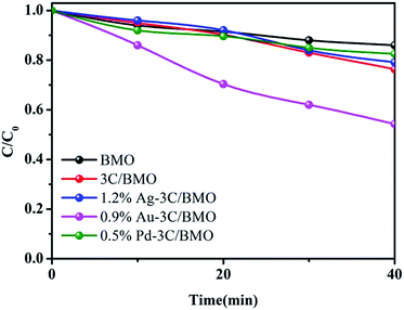 | ||
| Fig. 9 The photocatalytic activities of pristine BMO, 3C/BMO as well as various noble metals loaded samples toward RhB degradation by using a bandpass filter (550 nm) with luminous power of 500 W. | ||
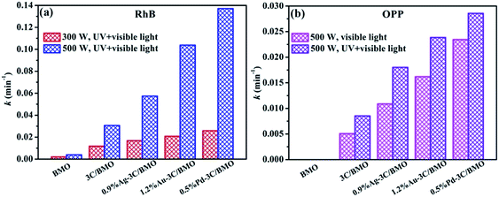
The photocatalytic processes toward RhB and OPP could be further quantitatively assessed through employing the pseudo-first-order kinetics, which is expressed as ln(C0/C) = kt, where C0 and C is the concentration of RhB or OPP at t = 0 and at time t, respectively. k is the pseudo-first-order rate constant, which can be obtained from the reduction of the peak intensity at 552 nm for RhB and 282 nm for OPP with increasing time. The photodegradation rates of RhB and OPP over different samples are shown in Fig. S17† and the calculated constant k are displayed in Fig. 10. As shown in Fig. 10a, the k values with luminous power of 500 W are considerably higher than the counterparts with luminous power of 300 W. For sample 0.5% Pd–3C/BMO, the k value (500 W) is nearly 5 times as that of value with luminous power of 300 W. Fig. 10b displays the degradation constants toward OPP under different light irradiation. Whether under visible light or UV + visible light irradiation, the k values of pristine Bi2MoO6 are nearly close to zero. After carbonate doping and noble metals loading, the maximum k value could reach 0.0234 and 0.0286 min−1 under visible light or UV + visible light irradiation, respectively.
3.3 Photocatalytic mechanism
To comprehensively understand the photocatalytic process, scavenger trapping experiments were conducted. Fig. 11 displays the results after adding various scavengers in the photodegradation process of RhB and OPP under visible light irradiation. Benzoquinone (BQ) employed as an ˙O2− scavenger, isopropanol (IPA) as an ˙OH scavenger, AgNO3 as a scavenger of e− and ammonium oxalate (AO) as the scavenger of h+, were added to the photocatalytic reaction system, respectively. Details of UV-visible absorption spectra recorded during photocatalytic degradation of OPP and the residual fraction of OPP in solution as a function of reaction time over 0.5% Pd–3C/BMO by adding various scavengers were given in Fig. S18.†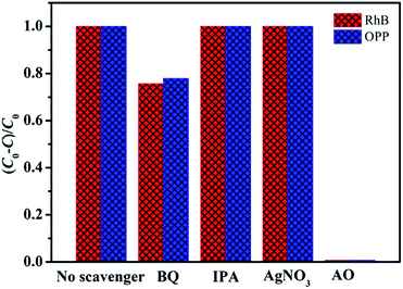 | ||
| Fig. 11 Effects of various scavengers on the photodegradation of RhB and OPP over 0.5% Pd–3C/BMO under UV + visible light and visible light irradiation, respectively. | ||
As shown in Fig. 11, it is clearly seen that the photodegradation of RhB and OPP are heavily depressed by adding AO and slightly inhibited after the addition of BQ. The participation of IPA and AgNO3 has no influence on the photocatalytic efficiency. This phenomenon reveals that h+ plays the dominant role in the photodegradation of RhB as well as OPP and ˙O2− properly contributes to the photocatalytic efficiency.
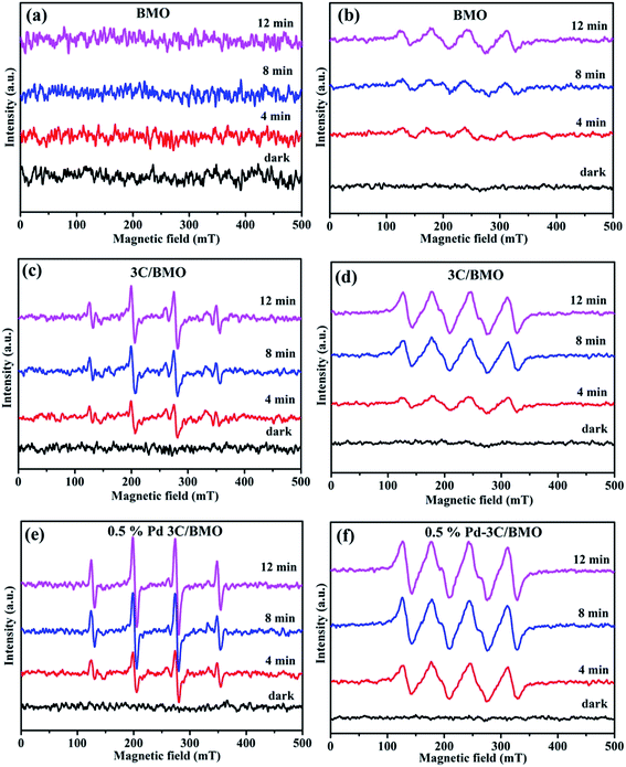
To further specify the active species involved in the photocatalytic process, ESR technique was carried and the results are shown in Fig. 12. In brief, DMPO was used as trapping agent to capture ˙O2− and ˙OH active species. For comparison, the ESR spectra of DMPO–˙O2− and DMPO–˙OH without photocatalysts were also measured, which results are shown in Fig. S19.† No signal of either DMPO–˙O2− or DMPO–˙OH was observed, indicating that active species of ˙O2− and ˙OH could not be produced without photocatalysts. As illustrated in Fig. 12, pristine BMO exhibited no apparent ESR signal of DMPO–˙OH even prolonging the irradiation time. Whereas the characteristic sextet peaks of DMPO–˙O2− ESR signal was observed with an increase of visible light irradiation time for Bi2MoO6 (Fig. 12b). As for 3C/BMO and 0.5% Pd–3C/BMO, the ESR signal of DMPO–˙OH appeared under visible light irradiation (Fig. 12c and e), predicting that CO32− doping and Pd loading can improve the capability of ˙OH generation for Bi2MoO6. Moreover, it is seen that the intensity of DMPO–˙O2− ESR signal also greatly increased after CO32− doping and noble metal loading (Fig. 12d and f). This observation hinted that CO32− doping in Bi2MoO6 can enhance the charge separation efficiency and the subsequent photocatalytic activity, which is verified by the following photocurrent measurement. In addition, noble metals loading can further improve the intensity of DMPO–˙OH and DMPO–˙O2− ESR signal, which can further increase the charge separation of photogenerated carriers as well the photocatalytic performance.
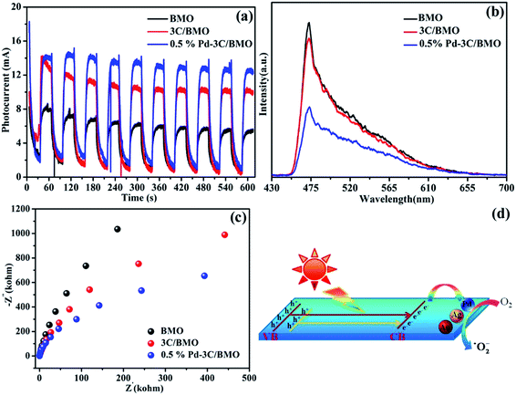
It is now necessary to specify the origin of the highly enhanced photocatalytic activity of Bi2MoO6 by CO32− doping and noble metals loading. Basically, several factors should be taken into consideration, including electronic structure, surface area, doping effects, cocatalysts and so forth. In view of solid state physics, any perturbation of lattice structure can have consequences on the electronic structure. By CO32− doping, upward valence band edge of Bi2MoO6 was achieved, which promises to weakened driving force of photogenerated holes. The higher valence band edge of Bi2MoO6 induces poor photocatalytic activity toward oxidation reaction, which is in contrast to the observed results in Fig. 10. Therefore, other factors should be responsible for the boosting photocatalytic activity of Bi2MoO6 by CO32− doping and noble metals loading. Since photocatalytic reaction occurs on semiconductor surfaces, the surface to volume ratio may impose great impact on the photocatalytic performance of Bi2MoO6 samples. For the present Bi2MoO6 samples, the BET surface areas are determined to be 52–57 m2 g−1 for noble metals loaded 3C/BMO samples, which are much larger than that of 1.8 m2 g−1 for pristine Bi2MoO6 sample. Principally, an increase of surface area leads to more active sites and enhances the photocatalytic activity of semiconductors. Hence, the increased surface areas of noble metals loaded 3C/BMO samples possibly contributed to the improvement of the photocatalytic activity, nearly being in accordance with the trend of the photocatalytic performance toward RhB and OPP degradation. As for doping effects, it is well accepted that the incorporation of foreign doping ions into semiconductors can have consequences on the microstructure, electronic structure as well as charge transfer process. Moreover, the impurity ions can not only decrease the photothreshold energy but also serve as trap centers for charge separation and improvement of electrical conductivity.57 The separation and transfer efficiency of the photogenerated charge carriers were explored using transient photocurrent responses with light on/off cycles. As illustrated in Fig. 13a, the photocurrent density of pure Bi2MoO6 reaches at about 6.25 mA, which was greatly improved to 10.48 mA after CO32− doping. Moreover, the photocurrent density was further increased to 13.54 mA via noble metal loading. Stronger photocurrent density often promises higher separation efficiencies of photogenerated electrons and holes.58 The improved charge separation efficiency of Bi2MoO6 after CO32− doping and noble metal loading was further investigated by photoluminescence spectra (Fig. 13b). As a self-activating phosphor, Bi2MoO6 exhibits a broad, intrinsic blue-green emission band centered at about 472 nm under UV light excitation. The incorporation of CO32− groups and noble metal loading on Bi2MoO6 caused efficient depression of the blue-green luminescence, which suggests promoted separation of photogenerated charge carriers and promises enhanced photocatalytic activity. The Nyquist plot data of the as-prepared samples were measured in order to investigate the process of electron transfer. As illustrated in Fig. 13c, the arc radius of the Nyquist plot of 3C/BMO sample is smaller than that of pure Bi2MoO6, implying a faster transfer rate of charge carriers in the former, leading to the effective separation of electron–hole pairs.59 Moreover, noble metal loading further improves the charge separation efficiency and the subsequent photocatalytic reactivity. As a consequence, the highly improved charge separation efficiency, charge transfer rate greatly enhance the photocatalytic activity. On the basis of the above results, a plausible photocatalytic mechanism was proposed, as illustrated in Fig. 13d. Under visible light or UV + visible light irradiation, the electrons are excited from valence band or defect states to conduction band of Bi2MoO6, which subsequently migrate to the surface of noble metals and are captured by O2 to produce ˙O2−. Subsequently, the holes remained in valence band and the photogenerated ˙O2− in conduction band are involved in the photocatalytic reaction.
4. Conclusions
Anionic group doping and noble metal loading as two promising strategies to construct a novel photocatalytic material for efficient photodegrading water organic pollutants. Carbonate doping induced the generation of oxygen vacancies and band gap narrowing, which are beneficial for visible light harvest and photogenerated charges separation. Nobel metals (Au, Ag and Pd) as cocatalysts further improved the photogenerated charges separation efficiency. By CO32− doping and noble metal loading, the photocatalytic activities of Bi2MoO6 toward RhB and OPP were enormously enhanced. The synthesized 0.5% Pd–3C/BMO photocatalyst is of potential importance for water organic pollutants.Acknowledgements
This work was supported by the National Natural Science Foundation of China (NSFC, 51462025).References
- S. F. Yang, C. G. Niu, F. W. Huang, H. Zhang, C. Liang and G. M. Zeng, Environ. Sci.: Nano, 2017, 4, 585–595 RSC.
- C. Yu, Z. Wu, R. Liu, D. D. Dionysiou, K. Yang, C. Wang and H. Liu, Appl. Catal., B, 2017, 209, 1–11 CrossRef CAS.
- F. Raziq, Y. Qu, M. Humayan, A. Zada, H. Yu and L. Jing, Appl. Catal., B, 2017, 201, 486–494 CrossRef CAS.
- Y. Liu, G. Zhu, J. Gao, M. Hojamberdiev, R. Zhu, X. Wei, Q. Guo and P. Liu, Appl. Catal., B, 2017, 200, 72–82 CrossRef CAS.
- X.-B. Zhang, L. Zhang, J.-S. Hu and X.-H. Huang, RSC Adv., 2016, 6, 32349–32357 RSC.
- H. Hirakawa, S. Shiota, Y. Shiraishi, H. Sakamoto, S. Ichikawa and T. Hirai, ACS Catal., 2016, 6, 4976–4982 CrossRef CAS.
- A. Etogo, R. Liu, J. Ren, L. Qi, C. Zheng, J. Ning, Y. Zhong and Y. Hu, J. Mater. Chem. A, 2016, 4, 13242–13250 CAS.
- W. Luo, Z. Li, T. Yu and Z. Zou, J. Phys. Chem. C, 2012, 116, 5076–5081 CAS.
- Y. Zhou, Z. Zhao, F. Wang, K. Cao, D. E. Doronkin, F. Dong and J.-D. Grunwaldt, J. Hazard. Mater., 2016, 307, 163–172 CrossRef CAS PubMed.
- Z. Dai, F. Qin, H. Zhao, J. Ding, Y. Liu and R. Chen, ACS Catal., 2016, 6, 3180–3192 CrossRef CAS.
- Y. Liu, G. Zhu, J. Gao, R. Zhu, M. Hojamberdiev, C. Wang, X. Wei and P. Liu, Appl. Catal., B, 2017, 205, 421–432 CrossRef CAS.
- Y. Fu, C. Chang, P. Chen, X. Chu and L. Zhu, J. Hazard. Mater., 2013, 254–255, 185–192 CrossRef CAS PubMed.
- M. Wang, C. Niu, Q. Liu, Y. Che and J. Liu, Mater. Sci. Semicond. Process., 2014, 25, 271–278 CrossRef CAS.
- H. Huang, X. Li, J. Wang, F. Dong, P. K. Chu, T. Zhang and Y. Zhang, ACS Catal., 2015, 5, 4094–4103 CrossRef CAS.
- Y. Huang, H. Li, W. Fan, F. Zhao, W. Qiu, H. Ji and Y. Tong, ACS Appl. Mater. Interfaces, 2016, 8, 27859–27867 CAS.
- W. J. Jo, J.-W. Jang, K.-J. Kong, H. J. Kang, J. Y. Kim, H. Jun, K. P. S. Parmar and J. S. Lee, Angew. Chem., Int. Ed., 2012, 51, 3147–3151 CrossRef CAS PubMed.
- C. Li, G. Chen, J. Sun, J. Rao, Z. Han, Y. Hu, W. Xing and C. Zhang, Appl. Catal., B, 2016, 188, 39–47 CrossRef CAS.
- Z. Dai, F. Qin, H. Zhao, F. Tian, Y. Liu and R. Chen, Nanoscale, 2015, 7, 11991–11999 RSC.
- C. Kongmark, R. Coulter, S. Cristol, A. Rubbens, C. Pirovano, A. Löfberg, G. Sankar, W. Beek, E. Bordes-Richard and R.-N. Vannier, Cryst. Growth Des., 2012, 12, 5994–6003 CAS.
- H. Li, W. Li, S. Gu, F. Wang, H. Zhou, X. Liu and C. Ren, RSC Adv., 2016, 6, 48089–48098 RSC.
- R. Kashfi-Sadabad, S. Yazdani, A. Alemi, T. D. Huan, R. Ramprasad and M. T. Pettes, Langmuir, 2016, 32, 10967–10976 CrossRef CAS PubMed.
- H. Li, W. Li, S. Gu, F. Wang and H. Zhou, Catal. Sci. Technol., 2016, 6, 3510–3519 CAS.
- D. Wang, H. Shen, L. Guo, C. Wang, F. Fu and Y. Liang, RSC Adv., 2016, 6, 71052–71060 RSC.
- T. Zhou, J. Hu and J. Li, Appl. Catal., B, 2011, 110, 221–230 CrossRef CAS.
- X. Ding, W. Ho, J. Shang and L. Zhang, Appl. Catal., B, 2016, 182, 316–325 CrossRef CAS.
- S. Li, X. Shen, J. Liu and L. Zhang, Environ. Sci.: Nano, 2017, 4, 1155–1167 RSC.
- J. Di, J. Xia, M. Ji, H. Li, H. Xu, H. Li and R. Chen, Nanoscale, 2015, 7, 11433–11443 RSC.
- Y. Chen, G. Tian, Y. Shi, Y. Xiao and H. Fu, Appl. Catal., B, 2015, 164, 40–47 CrossRef CAS.
- J. Li, Y. Yin, E. Liu, Y. Ma, J. Wan, J. Fan and X. Hu, J. Hazard. Mater., 2017, 321, 183–192 CrossRef CAS PubMed.
- D. Wang, H. Shen, L. Guo, F. Fu and Y. Liang, New J. Chem., 2016, 40, 8614–8624 RSC.
- B. Zhang, J. Li, Y. Gao, R. Chong, Z. Wang, L. Guo, X. Zhang and G. Li, J. Catal., 2017, 345, 96–103 CrossRef CAS.
- Z. Zhao, W. Zhang, Y. Sun, J. Yu, Y. Zhang, H. Wang, F. Dong and Z. Wu, J. Phys. Chem. C, 2016, 120, 11889–11898 CAS.
- R. M. Mohamed and F. M. Ibrahim, J. Ind. Eng. Chem., 2015, 22, 28–33 CrossRef CAS.
- X. Meng and Z. Zhang, Appl. Surf. Sci., 2017, 392, 169–180 CrossRef CAS.
- J. Wang, Y. Yu, S. Li, L. Guo, E. Wang and Y. Cao, J. Phys. Chem. C, 2013, 117, 27120–27126 CAS.
- F. D. Hardcastle and I. E. Wachs, J. Phys. Chem., 1991, 95, 10763–10772 CrossRef CAS.
- C. Kongmark, V. Martis, A. Rubbens, C. Pirovano, A. Lofberg, G. Sankar, E. Bordes-Richard, R.-N. Vannier and W. Van Beek, Chem. Commun., 2009, 32, 4850–4852 RSC.
- L. Zhang, T. Xu, X. Zhao and Y. Zhu, Appl. Catal., B, 2010, 98, 138–146 CrossRef CAS.
- Z. Zhang, H. Chen, C. Xing, M. Guo, F. Xu, X. Wang, H. J. Gruber, B. Zhang and J. Tang, Nano Res., 2011, 4, 599–611 CrossRef CAS.
- J. Li and C. Y. Liu, Eur. J. Inorg. Chem., 2010, 8, 1244–1248 CrossRef.
- J. Zhang, Y. Lu, L. Ge, C. Han, Y. Li and Y. Gao, Appl. Catal., B, 2017, 204, 385–393 CrossRef CAS.
- F. Dong, Q. Li, Y. Sun and W.-K. Ho, ACS Catal., 2014, 4, 4341–4350 CrossRef CAS.
- S. Zhu, S. Liang, Q. Gu, L. Xie, J. Wang, Z. Ding and P. Liu, Appl. Catal., B, 2012, 119–120, 146–155 CrossRef CAS.
- D. Wu, S. Yue, W. Wang, T. An, G. Li, H. Y. Yin, H. Zhao and P. K. Wong, Appl. Catal., B, 2016, 192, 35–45 CrossRef CAS.
- Y. Liu, G. Zhu, J. Gao, R. Zhu, M. Hojamberdiev, C. Wang, X. Wei and P. Liu, Appl. Catal., B, 2017, 205, 421–432 CrossRef CAS.
- D. Lu, B. Zhao, P. Fang, S. Zhai, D. Li, Z. Chen, W. Wu, W. Chai, Y. Wu and N. Qi, Appl. Surf. Sci., 2015, 359, 435–448 CrossRef CAS.
- M. T. Uddin, Y. Nicolas, C. Olivier, T. Toupance, L. Servant, M. M. Müller, H.-J. Kleebe, J. Ziegler and W. Jaegermann, Inorg. Chem., 2012, 51, 7764–7773 CrossRef CAS PubMed.
- M. Sun, Q. Zhao, C. Du and Z. Liu, RSC Adv., 2015, 5, 22740–22752 RSC.
- L. Ye, L. Zan, L. Tian, T. Peng and J. Zhang, Chem. Commun., 2011, 47, 6951–6953 RSC.
- M. Li, Y. Hu, S. Xie, Y. Huang, Y. Tong and X. Lu, Chem. Commun., 2014, 50, 4341–4343 RSC.
- J. Zhong, F. Chen and J. Zhang, J. Phys. Chem. C, 2010, 114, 933–939 CAS.
- J. Liu, L. Han, N. An, L. Xing, H. Ma, L. Cheng, J. Yang and Q. Zhang, Appl. Catal., B, 2017, 202, 642–652 CrossRef CAS.
- T. Xiong, H. Huang, Y. Sun and F. Dong, J. Mater. Chem. A, 2015, 3, 6118–6127 CAS.
- M. Long, W. Cai and H. Kish, Chem. Phys. Lett., 2008, 461, 102–105 CrossRef CAS.
- C. Ye, J. Li, Z. J. Li, X. B. Li, X. B. Fan, L. P. Zhang, B. Chen, C. H. Tung and L. Z. Wu, ACS Catal., 2015, 5, 6973–6979 CrossRef CAS.
- Y. Su, L. Peng, J. Guo, S. Huang, L. Lv and X. Wang, J. Phys. Chem. C, 2014, 118, 10728–10739 CAS.
- Y. Su, B. Zhu, K. Guan, S. Gao, L. Lv, C. Du, L. Peng, L. Hou and X. Wang, J. Phys. Chem. C, 2012, 116, 18508–18517 CAS.
- J. Zhang, Y. Ma, Y. Du, H. Jiang, D. Zhou and S. Dong, Appl. Catal., B, 2017, 209, 253–264 CrossRef CAS.
- J. Hou, H. Cheng, C. Yang, O. Takeda and H. Zhu, Nano Energy, 2015, 18, 143–153 CrossRef CAS.
Footnote |
| † Electronic supplementary information (ESI) available: Raman spectra, TG curves and FTIR spectra of carbonated doped samples; XRD patterns, XPS spectra, SEM and TEM images, BET analysis and photocatalytic properties of noble metals loaded samples. See DOI: 10.1039/c7ra04615d |
| This journal is © The Royal Society of Chemistry 2017 |

