 Open Access Article
Creative Commons Attribution 3.0 Unported Licence
Deep-red organic light-emitting diodes with stable electroluminescent spectra based on zinc complex host material
Yungui Li a,
Xiang Gao
 b,
Lei Wang
 a and
Guoli Tu*a
aWuhan National Laboratory for Optoelectronics, Huazhong University of Science and Technology, Wuhan, P. R. China. E-mail: tgl@hust.edu.cn
bSchool of Materials Science & Engineering, Hubei Key Laboratory of Plasma Chemistry and Advanced Materials, Wuhan Institute of Technology, Wuhan 430073, China
First published on 21st August 2017
Abstract
A zinc complex host material named Zn(PPI)2 (PPI = 2-(1-phenyl-1H-phenanthro[9,10-d]imidazol-2-yl)phenol) is synthesized by an improved strategy. Combined with dopant Ir(piq)3 and Ir(pmiq)2(acac), deep-red phosphorescent organic light-emitting diodes are fabricated and investigated. The devices show a highest external quantum efficiency of 9.5% based on Ir(piq)3 and 13.1% for Ir(pmiq)2(acac). All these devices show very stable electroluminescent spectra without significant shift during current density increase. Commission Internationale de l'Eclairage coordinates of (0.68, 0.32) and (0.70, 0.30) are obtained respectively.
Introduction
Organic light-emitting diodes (OLEDs) have gained significant attention after their invention by Tang and Vanslyke in 1987.1 With the introduction of phosphorescent2,3 and thermally activated delayed fluorescent (TADF) emitters,4,5 the internal quantum efficiency of phosphorescent OLEDs (PhOLEDs) can reach as high as 100%, which indicates unity energy conversion. The development of organic doping technology,6 exciton blocking layers7 and light extraction strategies8 bring white PhOLEDs to a level with comparable with the power efficiency of fluorescent tubes.9 After decades of effort, OLEDs have now been used in display panels and light sources.Increasing interest have been paid to deep-red and near-infrared OLEDs because of their potential application in fields like phototherapy,10 telecommunication11 and defense.12 However, the external quantum efficiency (EQE) of deep-red OLEDs with Commission Internationale de l'Eclairage (CIE) coordinate CIE x ≥ 0.70 is still low. What is more, the CIE coordinate under high current density is rarely discussed in previous reports. Under high current density, the shift of recombination zone could lead to blue shift, giving rise to emission with lower CIE x value.13
The key issues to obtain an ideal deep-red devices with CIE x ≥ 0.7 are the emission peak wavelength and the bandwidth of spectrum.14 To get emission with a stable CIE coordinate, device needs to have balanced hole and electron injection, and stable recombination zone without significant shift at high current density. To meet these requirements, both material and device configuration should be carefully optimized.
Fujii et al. realized a deep-red OLEDs with EQE of 10.2% and CIE coordinates of (0.70, 0.27), by using a deep-red phosphorescent emitter bis(2,3-diphenylquinoxaline)iridium-(acetylacetone) [(QH)2Ir(acac)] and 3-(4-biphenylyl)-4-phenyl-5-(4-tert-butylphenyl)-1,2,4-triazole (TAZ-01) as host.15 However, the CIE coordinate shifted to lower than 0.70 when increasing current density. Jou et al. reported a deep-red OLED with [bis(spirofluorenedibenzosuberene[d]quinoxaline-C2,N)-monoacetyl-cetone]iridium(III) as emitter and N,N′-di(naphthalene-1-yl)-N,N′-diphenylbenzidine (NPD) and bis(10-hydroxybenzo[h]quinolinato)beryllium (BeBq2) as co-host, achieving maximum EQE of 11.2%, and CIE coordinates of (0.70, 0.27) at 10 cd m−2.16 However, the CIE coordinates moved to (0.67, 0.26) when the luminance increased to 500 cd m−2. Wang et al. reported a deep-red OLED with TADF emitter 7,10-bis(4-(diphenylamino)phenyl)dibenzo[f,h]quinoxaline-2,3-dicarbo-nitrile (TPA-DCPP). Its nondoped OLED device showed maximum EQE of 2.1% with CIE coordinated of (0.70, 0.29). When 20 wt% TPA-DCPP doped in TPBi as emitting layer, OLED exhibited a maximum EQE of 9.8% with CIE coordinate of (0.68, 0.32).17 Recently, Yuji et al. reported an exciplex system with bis(2,3-diphenylquinoxaline)iridium(dipivaloyl-methane) [(DPQ)2Ir(dpm)] emitter for deep-red OLEDs. Co-deposited di(naphthalene-1-yl)-N,N′-diphenylbenzidine (NPD) and 2-(3′-(dibenzo[b,d]thiophen-4-yl)-[1,1′-biphenyl]-3-yl)-4,6-diphenyl-1,3,5-triazine (4DBT46TRZ) as host, maximum EQE of 17.9% with CIE coordinates of (0.70, 0.29) at 100 cd m−2 was obtained.18 However, there is no information about CIE coordinate under high current density.
All these host materials were obtained via multi-step synthesis process, which hinders their commercial application because of the synthetic complexity. Adachi et al. reported a zinc complex bis[2-(2-benzothiazoyl)phenolato]zinc(II) [Zn(BTP)2] as host material with Ir(piq)3 dopant for deep-red OLEDs, realizing device performance with maximum EQE of 10.3%. At a current density of 10 mA cm−2, CIE coordinate of (0.67, 0.33) was obtained. Devices with this zinc complex host material showed higher performance compared to 4,4′-bis(9-carbazolyl)-2,2′-biphenyl (CBP) based devices, but the CIE coordinate at high current density and the color stability were not showed.19 According to their research, zinc complex host material Zn(BTP)2 showed better charge carrier injection properties than CBP. Recently, Wang et al. realized blue, green and orange-red devices based on zinc and beryllium complex host with ligand of 2-(1-phenyl-1H-phenanthro[9,10-d]imidazol-2-yl)phenol (PPIH). For organic red PhOLEDs based on Zn(PPI)2 as host material and bis(2-methyldibenzo-[f,h]quinoxaline)acetylac-etonate iridium(III) (Ir(MDQ)2(acac)) as dopant, maximum EQE of 15.2% and CIE coordinate of (0.64, 0.36) have obtained. The zinc complex host material shows bipolar property of transporting electrons and holes, which facilitates charge balance. However, they used inorganic base sodium hydroxide to synthesize the complex in organic solvent, leading to modest yield (48%). Low solubility of sodium hydroxide and ligand PPIH in methanol causes difficulty for further purification.20 In the interest of simplifying the purification process and increasing product yield, an improved strategy for this zinc complex host is needed. More importantly, there is a lack of investigation on deep-red PhOLEDs and the electroluminescent spectrum stability of those devices with Zn(PPI)2 as host material.
Here, we reported efficient deep-red OLEDs with stable CIE x ≥ 0.7 based on Zn(PPI)2. An improved synthesis method for Zn(PPI)2 is developed and it is used as a host material for PhOLEDs with dopant Ir(piq)3 and Ir(pmiq)2(acac), to obtain deep-red OLEDs with CIE x ≥ 0.7. Rather than using poorly soluble inorganic base sodium hydroxide to adjust pH, we utilize trimethylamine combined with ethanol as solvent to synthesize Zn(PPI)2 complex. The zinc complex material is easily obtained by two steps, with slightly higher product yield of 60% by simple filter separation. This is among high product yield for zinc complex synthesis.21 When this zinc complex is used as host material for deep-red PhOLEDs with Ir(piq)3 emitter, maximum EQE of 9.5% with CIE coordinate of (0.68, 0.32) is achieved. It shows very stable electroluminescent emission, peaking at 636 nm without significant change of CIE coordinate when increasing current density. The CIE coordinate changes smaller than 0.005 when current density increases from 0.1 mA cm−2 to 100 mA cm−2. Maximum luminance above 10![[thin space (1/6-em)]](https://www.rsc.org/images/entities/char_2009.gif) 000 cd m−2 is obtained before device failure. Combined with emitter Ir(pmiq)2(acac), Zn(PPI)2 based deep-red OLEDs achieve maximum EQE of 13.1% with CIE coordinate of (0.70, 0.30). Highest luminance of 7261 cd m−2 is achieved. The device also shows very stable electroluminescent emission, peaking at 640 nm without significant change of CIE coordinate when increasing current density.
000 cd m−2 is obtained before device failure. Combined with emitter Ir(pmiq)2(acac), Zn(PPI)2 based deep-red OLEDs achieve maximum EQE of 13.1% with CIE coordinate of (0.70, 0.30). Highest luminance of 7261 cd m−2 is achieved. The device also shows very stable electroluminescent emission, peaking at 640 nm without significant change of CIE coordinate when increasing current density.
Experimental
Material synthesis
Ligand PPIH is synthesized according to literature.20 To further get zinc complex, 600 mg (1.55 mmol) PPIH is dissolved in 300 ml ethanol under 60 °C. 660 mg (6.52 mmol) trimethylamine is added, followed by adding Zn(OAc)2·2H2O (171 mg, 0.779 mmol). The mixture is stirred by magnetic stirring bar for 3 h before cooling down to room temperature. White crystal is found at the bottom of flask overnight. The product Zn(PPI)2 is filtered 3 days later and washed by ethanol. 1H NMR (400 MHz, [D6]DMSO): δ = 8.90 (d, 2H, J = 8.4 Hz), 8.06 (d, 2H, J = 7.8 Hz), 7.97 (d, 2H, J = 8.4 Hz), 7.85–7.67 (m, 10H), 7.52 (t, 2H, J = 7.8 Hz), 7.34–7.15 (m, 4H), 7.13 (t, 2H, J = 7.8 Hz), 6.93 (t, 2H, J = 8.1 Hz), 6.88 (d, 2H, J = 7.8 Hz), 6.79 (t, 4H, J = 9 Hz), 6.27 (t, 2H, J = 7.5 Hz).OLEDs fabrication
Zinc complex host material is purified twice by sublimation before device fabrication. Substrates with pre-patterned ITO are cleaned with acetone, ethanol and de-ionized water by ultrasonic bath for 10 min in each step. The substrates are then dried by dry nitrogen gas flow and oven at 120 °C. The devices with Ir(piq)3 are fabricated in vacuum chambers under 5 × 10⁻⁴ Pa. For device with emitter Ir(piq)3, the configuration is: ITO/MoO3 (10 nm)/NPB (x nm)/TCTA (5 nm)/Zn(PPI)2: 8 wt%. Ir(piq)3 (30 nm)/TPBi (y nm)/LiF (1 nm)/Al. For emitter Ir(pmiq)2(acac), device structure is ITO/MoO3 (8 nm)/TAPC (120 nm)/TCTA (5 nm)/Zn(PPI)2: 1 wt% Ir(pmiq)2(acac) (40 nm)/TPBi (5 nm)/Bphen (80 nm)/LiF (1 nm)/Al. Oxygen plasma treated (5 min) indium tin oxide (ITO) is used as anode, molybdenum oxide (MoO3) is used as hole injection layer, 1,1-bis[(di-4-tolylamino)phenyl]cyclohexane (TAPC) and N,N-di(naphthalen-1-yl)-N,N-diphenyl-benzidine (NPB) as hole transport layer, 4,4,4-tris(carbazol-9-yl)-triphenylamine (TCTA) and 2,2,2-(1,3,5-phenylen)-tris(1-phenyl-1H-benzimidazol) (TPBi) as exciton blocking layer, Zn(PPI)2 doped with Ir(piq)3 or Ir(pmiq)2(acac) as emission layer, TPBi and 4,7-diphenyl-1,10-phenanthroline (BPhen) as electron transport layer. Lithium fluoride (LiF) is used as electron injection layer and 100 nm aluminum as top electrode. Pixel size is 0.3 mm by 0.3 mm.Measurement
PL spectra are recorded by Edinburgh instruments (FLS 920 spectrometers) and UV-Vis absorption spectrum is measured by Shimadzu UV-Vis-NIR Spectrophotometer (UV-3600). 1H nuclear magnetic resonance (NMR) measurements was carried out with Bruker 400 MHz DRX spectrometer. All the devices are characterized immediately after fabrication in ambient environment without further encapsulation. Luminance, EL spectra and CIE coordinate information are measured by a PHOTO RESEARCH SpectraScan PR655 photometer and KEITHLEY 2400 SourceMeter as current source. The EL spectra and CIE coordinate, as well as luminance are recorded at each measurement step.Results and discussion
Zn(PPI)2
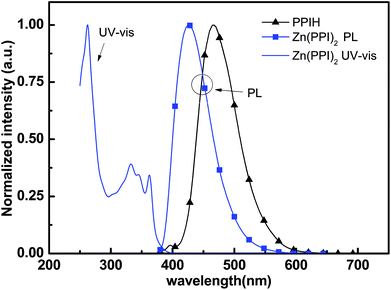
The synthetic route to zinc complex material is shown in Scheme 1. This zinc complex is obtained by utilizing trimethylamine with ethanol as solvent, since trimethylamine has better solubility than inorganic base. The yield is 60%, which is higher than previous reported method.20 The main reason for the increase of product yield is ligand PPIH and trimethylamine have slightly better solubility in ethanol than PPIH and inorganic base in methanol.Fig. 1 shows the physical properties including UV-Vis absorption and PL spectrum of Zn(PPI)2. Fig. 1 is the normalized UV-Vis absorption spectrum for Zn(PPI)2 and PL spectra for both Zn(PPI)2 and ligand PPIH. The spectra are recorded with a solution of these compounds about 10−5 mmol L−1 in CH2Cl2 at room temperature. For absorption spectrum, main peak at around 260 nm can be assigned to the π → π* transition of the benzene ring. Weak absorption band is found from 300 to 400 nm with two weaker peaks. This can attribute to the delocalized π → π* transition from ligand part in which the 2-substituted phenolate to the N-phenyl phenanthroimidazole ring.20 For zinc complex at room temperature, the PL spectrum covers wide range from 380 nm to 550 nm with a peak at 429 nm. However, ligand PPIH gives PL spectrum with peak at 467 nm.
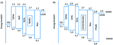
Deep-red OLED devices based on Zn(PPI)2
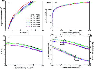
Fig. 2 shows the energy diagram for deep-red PhOLEDs, both for device with emitter Ir(piq)3 and Ir(pmiq)2(acac). The energy level data is collected from literatures.20,22,23 We firstly investigate deep-red OLEDs with Ir(piq)3 as guest material. HOMO level of Zn(PPI)2 is located at 5.8 eV and LUMO level at 2.7 eV, finely confining the energy gap of dopant Ir(piq)3. The triplet energy level of host is 2.67 eV, which is higher than dopant Ir(piq)3 at 2.05 eV,23 so triplet energy can transfer from host to guest. Devices are fabricated with the configuration of: ITO/MoO3 (10 nm)/NPB (x nm)/TCTA (5 nm)/Zn(PPI)2: 8 wt%. Ir(piq)3 (30 nm)/TPBi (y nm)/LiF (1 nm)/Al. Here, the thicknesses of NPB and TPBi are slightly optimized to obtain optimized device performance and to investigate the influence of current injection on EL spectra stability.Fig. 3 shows PhOLEDs device performance based on Zn(PPI)2 and Ir(piq)3, with variation of NPB (x nm) and TPBi (y nm) thickness. NPB thickness is changed from 50 nm to 60 nm and 70 nm, while TPBi is varied between 30 nm and 40 nm, to slightly change the injection and keep recombination zone within the emission layer.20 Fig. 3(a) exhibits the relation between driving voltages and current density for these devices. The current density changes slightly when optimizing hole and electron transport layers' thickness. For device with 50 nm NPB (x = 50 nm) and 30 nm TPBi (y = 30 nm), it gives highest current density under the same driving voltage among all devices. When increasing thickness of either NPB or TPBi, devices show lower current density. This could result from the resistance of organic layer.24 When NPB and TPBi are used as non-doped hole and electron transport layer, increasing transport layer thickness rises up device resistance and hinder the charge transport, which leads to lower current density.25
Fig. 3(b) shows the luminance behavior under different current densities for devices based on Zn(PPI)2 and Ir(piq)3. For all devices, maximum luminance is higher than 10![[thin space (1/6-em)]](https://www.rsc.org/images/entities/char_2009.gif) 000 cd m−2. These devices give similar current density and luminance curves. For device with 50 nm NPB (x = 50 nm) and 40 nm TPBi (y = 40 nm), the turn-on voltage (voltage for luminance at 1 cd m−2) is 2.7 V. The device reaches 100 cd m−2 under very low current density about 2.5 mA cm−2 and 1000 cd m−2 at 26 mA cm−2. The luminance further increases to 10
000 cd m−2. These devices give similar current density and luminance curves. For device with 50 nm NPB (x = 50 nm) and 40 nm TPBi (y = 40 nm), the turn-on voltage (voltage for luminance at 1 cd m−2) is 2.7 V. The device reaches 100 cd m−2 under very low current density about 2.5 mA cm−2 and 1000 cd m−2 at 26 mA cm−2. The luminance further increases to 10![[thin space (1/6-em)]](https://www.rsc.org/images/entities/char_2009.gif) 000 cd m−2 when the current density is about 300 mA cm−2. Maximum luminance about 20
000 cd m−2 when the current density is about 300 mA cm−2. Maximum luminance about 20![[thin space (1/6-em)]](https://www.rsc.org/images/entities/char_2009.gif) 000 cd m−2 can be obtained at 400 mA cm−2 before catastrophic device failure.
000 cd m−2 can be obtained at 400 mA cm−2 before catastrophic device failure.
The thickness of charge transport layer plays an important role on charge injection balance and recombination zone location, therefore it could influence device efficiency and color stability under high current density.6 In Fig. 3(c) and (d), we notice that under the same current density, devices with 50 nm NPB (x = 50 nm) and 40 nm TPBi (y = 40 nm) gives highest external quantum efficiency (EQE) and highest current efficiency. While for devices with 70 nm NPB (x = 70 nm) and 30 nm TPBi (y = 30 nm), lowest EQE or current efficiency is obtained, because of unbalanced charge injection. Highest EQE of 9.5% is obtained by 50 nm NPB (x = 50 nm) and 40 nm TPBi (y = 40 nm), devices, with current efficiency of 5.35 cd A−1 and power efficiency of 6.21 l m W−1. This could attribute to balanced charge recombination and well confinement of excitons within emission layer. The EQE is rolling down when increasing current density, which may result from triplet–triplet annihilation and triplet–polaron quenching.26
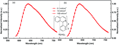
Fig. 4 summarizes the typical EL spectra for devices with Ir(piq)3 under current density from 0.1 mA cm−2 to 100 mA cm−2. Fig. 4(a) shows EL spectra of device with 50 nm NPB (x = 50 nm) and 40 nm TPBi (y = 40 nm), which gives the best device efficiency. Fig. 4(b) illustrates EL spectra of device with 50 nm NPB (x = 50 nm) and 30 nm TPBi (y = 40 nm), which has lowest injection resistance. All these EL spectra peak at 636 nm, with full width at half maximum (FWHM) about 100 nm. The CIE coordinates are (0.68, 0.32) for current density from 0.1 mA cm−2 to 100 mA cm−2. In this range, the CIE coordinate shifts smaller than 0.005. Fig. 4(a) indicates the device with balanced charge injection and fine exciton confinement configuration can exhibit extremely stable EL spectra even under high driving current density of 100 mA cm−2. Meanwhile, Fig. 4(b) indicates that even electron and hole is slightly unbalanced, no observable EL spectra change is found with increased driving voltage and a very small change of CIE coordinates.
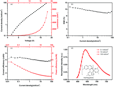
Based on the investigation on Ir(piq)3 emitter, we further study the performance of deep-red devices with Ir(pmiq)2(acac).22 Fig. 5(a) shows the devices' voltage–current density–luminance curves. The turn-on voltage is 3.7 V and device can reach maximum luminance of 7262 cd m−2 under 18.5 V before device failure. Higher turn-on voltage compared to Ir(piq)3 based device can attribute to thicker device layers. As we can see from Fig. 5(b), the maximum EQE of 13.1% is achieved. EQE rolls down a little to about 10% at 80–100 mA cm−2, which is a small roll-off compared with the same guest material doped in other host materials.22 The maximum current efficiency is 6.8 cd A−1 and the maximum power efficiency is 5.4 l m W−1. The EL spectra stability is showed in Fig. 5(d). As we can see, there is no significant shift for EL spectra with peak at 640 nm. The CIE coordinate is (0.70, 0.30) and the change of CIE coordinate is smaller than 0.004 from 0.1 mA cm−2 to 100 mA cm−2. Deep-red device based on Zn(PPI)2 and Ir(pmiq)2(acac) also shows very stable EL spectra stability and slightly higher EQE than device based on Ir(piq)3.
Good efficiency and stable EL property for these deep-red device are the results of these possible reasons: (1) the bipolar property of this Zn(PPI)2 host material facilitates the charge balance within the device; (2) with the blocking layer, the emission zone is well confined within the emission layer even under high current density.20 Possible reasons attribute to EQE difference for Ir(mpiq)2(acac) and Ir(piq)3 based device could be difference of device configuration, intrinsic quantum efficiency27 or dipole orientation.28 For deep-red OLEDs, two reasons can attribute to lower efficiency compared to blue, green, orange-red OLEDs: firstly, the nonradiative decay rate of emitter increases when the energy gap is decreasing according to energy gap law;29 secondly, a drop of luminous flux within the deep-red region and decrease of eye sensitivity among this wavelength range, leads to lower power efficiency compared to green or blue OLEDs.30 Compared to reported results,15,17,18 our devices show good performance among deep-red OLEDs, with stable CIE coordinate as high as (0.70, 0.30) even at high current density.
Conclusions
In conclusion, zinc complex host material named Zn(PPI)2 is synthesized by an improved strategy, with slightly higher product yield of 60% by two steps and easy purification. Deep-red PhOLEDs are fabricated based on host Zn(PPI)2 and dopant Ir(piq)3 and Ir(pmiq)2(acac). Highest EQE of 9.5% is obtained for Ir(piq)3 based device and 13.1% for Ir(pmiq)2(acac) device. These devices show deep red emission with CIE x of 0.67 for Ir(piq)3 and 0.70 for Ir(pmiq)2(acac) emitter. Devices with host Zn(PPI)2 and dopant Ir(piq)3 and Ir(pmiq)2(acac) exhibit very stable electroluminescent spectra and barely CIE coordinates shift when increasing current density. The results will provide a clue towards further development of efficient and stable deep-red OLEDs.Conflicts of interest
There are no conflicts to declare.Acknowledgements
This work was supported by the National Natural Science Foundation of China (Grant No. 21574049) and the National High Technology Research and Development Program of China (863 program, No. 2015AA033404).The authors thank for Dr Zaifei Ma, Dr Simone Lenk and Yuan Liu for beneficial discussion in Dresden Integrated Center for Applied Physics and Photonic Materials (IAPP) at TU Dresden. We also thank the HUST Analytical and Testing Center for material characterization and related measurements.References
- C. W. Tang and S. A. Vanslyke, Organic electroluminescent diodes, Appl. Phys. Lett., 1987, 51, 913–915 CrossRef CAS.
- C. Adachi, M. A. Baldo, M. E. Thompson and S. R. Forrest, Nearly 100% internal phosphorescence efficiency in an organic light-emitting device, J. Appl. Phys., 2001, 90, 5048–5051 CrossRef CAS.
- M. A. Baldo, D. F. O'Brien, Y. You, A. Shoustikov, S. Sibley and M. E. Thompson, et al., Highly efficient phosphorescent emission from organic electroluminescent devices, Nature, 1998, 395, 151–154 CrossRef CAS.
- H. Kaji, et al., Purely organic electroluminescent material realizing 100% conversion from electricity to light, Nat. Commun., 2015, 6, 8476 CrossRef CAS PubMed.
- H. Uoyama, K. Goushi, K. Shizu, H. Nomura and C. Adachi, Highly efficient organic light-emitting diodes from delayed fluorescence, Nature, 2012, 492, 234–238 CrossRef CAS PubMed.
- K. Walzer, B. Maennig, M. Pfeiffer and K. Leo, Highly efficient organic devices based on electrically doped transport layers, Chem. Rev., 2007, 107, 1233–1271 CrossRef CAS PubMed.
- M. Ikai, S. Tokito, Y. Sakamoto, T. Suzuki and Y. Taga, Highly efficient phosphorescence from organic light-emitting devices with an exciton-block layer, Appl. Phys. Lett., 2001, 79, 156–158 CrossRef CAS.
- M. C. Gather and S. Reineke, Recent advances in light outcoupling from white organic light-emitting diodes, J. Photonics Energy, 2015, 5, 057607 CrossRef.
- S. Reineke, F. Lindner, G. Schwartz, N. Seidler, K. Walzer and B. Lussem, et al., White organic light-emitting diodes with fluorescent tube efficiency, Nature, 2009, 459, 234–238 CrossRef CAS PubMed.
- C. L. Ho, H. Li and W. Y. Wong, Red to near-infrared organometallic phosphorescent dyes for OLED applications, J. Organomet. Chem., 2014, 751, 261–285 CrossRef CAS.
- J. C. G. Bünzli and S. V. Eliseeva, Lanthanide NIR luminescence for telecommunications, bioanalyses and solar energy conversion, J. Rare Earths, 2010, 28, 824–842 CrossRef.
- A. Rogalski and K. Chrzanowski, Infrared devices and techniques (revision), Metrology and Measurement Systems, 2014, 21, 565–618 CrossRef.
- D. H. Kim, N. S. Cho, H.-Y. Oh, J. H. Yang, W. S. Jeon and J. S. Park, et al., Highly Efficient Red Phosphorescent Dopants in Organic Light-Emitting Devices, Adv. Mater., 2011, 23, 2721–2726 CrossRef CAS PubMed.
- C. H. Fan, P. Sun, T. H. Su and C. H. Cheng, Host and dopant materials for idealized deep-red organic electrophosphorescence devices, Adv. Mater., 2011, 23, 2981–2985 CrossRef CAS PubMed.
- H. Fujii, H. Sakurai, K. Tani, K. Wakisaka and T. Hirao, Bright and ultimately pure red electrophosphorescent diode bearing diphenylquinoxaline, IEICE Electronics Express, 2005, 2, 260–266 CrossRef.
- J. H. Jou, Y. T. Su, M. T. Hsiao, H. H. Yu, Z. K. He and S. C. Fu, et al., Solution-Process-Feasible Deep-Red Phosphorescent Emitter, J. Phys. Chem. C, 2016, 120, 18794–18802 CAS.
- S. Wang, X. Yan, Z. Cheng, H. Zhang, Y. Liu and Y. Wang, Highly Efficient Near-Infrared Delayed Fluorescence Organic Light Emitting Diodes Using a Phenanthrene-Based Charge-Transfer Compound, Angew. Chem., Int. Ed., 2015, 54, 13068–13072 CrossRef CAS PubMed.
- Y. Nagai, H. Sasabe, J. Takahashi, N. Onuma, T. Ito and S. Ohisa, et al., Highly efficient, deep-red organic light-emitting devices using energy transfer from exciplexes, J. Mater. Chem. C, 2017, 5, 527–530 RSC.
- H. Kanno, K. Ishikawa, Y. Nishio, A. Endo, C. Adachi and K. Shibata, Highly efficient and stable red phosphorescent organic light-emitting device using bis[2-(2-benzothiazoyl)phenolato]zinc(II) as host material, Appl. Phys. Lett., 2007, 90, 1–4 CrossRef.
- K. Wang, F. Zhao, C. Wang, S. Chen, D. Chen and H. Zhang, et al., High-performance red, green, and blue electroluminescent devices based on blue emitters with small singlet-triplet splitting and ambipolar transport property, Adv. Funct. Mater., 2013, 23, 2672–2680 CrossRef CAS.
- C. S. Oh, C. W. Lee and J. Y. Lee, Simple heteroatom engineering for tuning the triplet energy of organometallic host materials for red, green and blue phosphorescent organic light-emitting diodes, Chem. Commun., 2013, 49, 3875–3877 RSC.
- Y. Li, W. Zhang, L. Zhang, X. Wen, Y. Yin and S. Liu, et al., Ultra-high general and special color rendering index white organic light-emitting device based on a deep red phosphorescent dye, Org. Electron., 2013, 14, 3201–3205 CrossRef CAS.
- A. Tsuboyama, H. Iwawaki, M. Furugori, T. Mukaide, J. Kamatani and S. Igawa, et al., Homoleptic Cyclometalated Iridium Complexes with Highly Efficient Red Phosphorescence and Application to Organic Light-Emitting Diode, J. Am. Chem. Soc., 2003, 125, 12971–12979 CrossRef CAS PubMed.
- J. Blochwitz, M. Pfeiffer, T. Fritz and K. Leo, Low voltage organic light emitting diodes featuring doped phthalocyanine as hole transport material, Appl. Phys. Lett., 1998, 73, 729–731 CrossRef CAS.
- R. Meerheim, B. Luessem and K. Leo, Efficiency and Stability of p-i-n Type Organic Light Emitting Diodes for Display and Lighting Applications, Proc. IEEE, 2009, 97, 1606–1626 CrossRef CAS.
- S. Reineke, K. Walzer and K. Leo, Triplet-exciton quenching in organic phosphorescent light-emitting diodes with Ir-based emitters, Phys. Rev. B: Condens. Matter Mater. Phys., 2007, 75, 1–13 CrossRef.
- M. Furno, R. Meerheim, S. Hofmann, B. Lüssem and K. Leo, Efficiency and rate of spontaneous emission in organic electroluminescent devices, Phys. Rev. B: Condens. Matter Mater. Phys., 2012, 85, 1–21 CrossRef.
- M. J. Jurow, C. Mayr, T. D. Schmidt, T. Lampe, P. I. Djurovich and W. Brütting, et al., Understanding and predicting the orientation of heteroleptic phosphors in organic light-emitting materials, Nat. Mater., 2016, 15, 85–91 CrossRef CAS PubMed.
- J. V. Caspar and T. J. Meyer, Application of the Energy Gap Law to Excited-State Decay, J. Phys. Chem., 1983, 87, 952–957 CrossRef CAS.
- S. R. Forrest, D. D. C. Bradley and M. E. Thompson, Measuring the efficiency of organic light-emitting devices, Adv. Mater., 2003, 15, 1043–1048 CrossRef CAS.
| This journal is © The Royal Society of Chemistry 2017 |


