 Open Access Article
Electron beam induced epitaxial crystallization in a conducting and insulating a-LaAlO3/SrTiO3 system†
Gwangyeob Lee ab,
Seon Young Moonc,
Jinyeon Kimad,
Seung-Hyub Baek
 ce,
Do Hyang Kimb,
Ho Won Jang
 d and
Hye Jung Chang*ae
aAdvanced Analysis Center, Korea Institute of Science and Technology, Seoul 02792, South Korea. E-mail: almacore@kist.re.kr
bDepartment of Materials Science and Engineering, Yonsei University, Seoul 03722, South Korea
cElectronic Materials Research Center, Korea Institute of Science and Technology, Seoul 02792, South Korea
dDepartment of Materials Science and Engineering and Research Institute of Advanced Materials, Seoul National University, Seoul 08826, South Korea
eDepartment of Nanomaterials Science and Technology, University of Science and Technology, Daejeon 34113, South Korea
First published on 17th August 2017
Abstract
Interfacial conductivity at the interface between two insulating oxides, that is 2DEG, shows a number of intriguing properties and applications, such as on/off switching with external electric fields, use in nanoscale electronic devices and tunable conductivity. Here, we report the effect of the interfacial conductivity on the kinetic behavior of electron-beam-induced epitaxial crystallization of an oxide amorphous thin film on an SrTiO3 substrate. Epitaxial growth from the interface can occur without direct e-beam irradiation at the interface due to accumulated charge around the beam position in the insulating materials. 2DEG, which acts as a current path delays the crystallization kinetics, thus delicate control of the crystallized pattern shape and size is available. As a result, successful pattern writing with a width of about 5 nm was performed. The present work provides useful guidelines for coherent atomic scale e-beam patterning considering the critical distance of the electron beam from the interface for the epitaxial growth, e-beam dose rate effect on the growth rate and the heterostructure interfacial conductivity.
Introduction
With the recent rapid progress in nanotechnology, device structures have become miniaturized, and the demand for fabricating and manipulating nanostructures has dramatically increased. Conventional photolithography, mostly applied to the manufacturing of semiconductor microchips and the fabrication of microelectromechanical systems (MEMS) devices, uses a light source that is not suitable for nanofabrication because of limitations such as the wavelength of light or diffraction issues.1 For many years, other lithography techniques utilizing various sources including X-ray, electron beam (e-beam), and ion-beam sources have been investigated to obtain better performance.2–5 Of these techniques, e-beam lithography (EBL) is one of the most promising for nanoscale patterning owing to its excellent resolution and maskless patterning. However, it is still challenging to fabricate nanostructures with dimensions of several nanometers because electrons are backscattered within the substrate over a large radius, even though the EBL technique used in scanning electron microscopy (SEM) has reached sub-10 nm patterns.3,6–8In contrast, the e-beam-induced microstructural changes in transmission electron microscopy (TEM) can be applied to attain more precise nanoscale patterning as small as a few nanometers, overcoming the limited resolution of EBL in SEM.9–11 In general, the interaction between the accelerated electrons and the specimen in TEM can cause several changes in the materials, such as defect generation, amorphization, and crystallization.12–16 It is well known that the point defects generated via knock-on damage play a crucial role in the crystallization of amorphous materials and the phase transitions of crystalline materials; that is, the point defects created by the elastic scattering of electrons induce a rearrangement of existing unstable atomic bonds.12,17,18 For example, real-time TEM imaging revealed that the structural transition of La2/3Sr1/3MnO3 with the perovskite ABO3 structure into Brownmillerite was caused by e-beam-induced oxygen vacancies.19 Moreover, the amorphous regions in Si, Ge, GaAs, and InP were crystallized by the bombardment of accelerated electrons.20–23 The unexpected structural changes by e-beam irradiation during TEM, on the other hand, can be applied in a useful way for nanoarchitectonics—the creation and manipulation of new nanomaterials by controlling atoms or molecules.24 Recently, atomic-scale patterning using a focused e-beam probe in scanning transmission electron microscopy (STEM) has been suggested for graphene and amorphous oxide thin films.9–11,25 For instance, Song et al. demonstrated the atomic-scale sculpting of graphene using a focused e-beam, and Liu et al. observed the in-plane growth of graphene in STEM. Jesse et al. also presented a nanoscale sculpture of crystalline SrTiO3 by controlling a focused e-beam during STEM.
In this study, we demonstrate the e-beam-controlled crystallization of an amorphous LaAlO3 (a-LAO) thin film grown epitaxially at the LaAlO3/SrTiO3-substrate interface and investigate the origin of e-beam-induced crystallization in the insulating oxide materials. Epitaxial crystallization from the interface occurs when the e-beam is located within a critical distance from the interface, and its kinetics can be controlled by the interfacial conductivity and e-beam dose rate. The model LAO/STO system is interesting owing to its unique physical properties, which include a high electron mobility at the interface, i.e., a two-dimensional electron gas (2DEG).26–28 The formation of a conductive interface has been reported in several crystalline (c) oxide heterostructures: LAO/STO, ZnO/ZnMgO, and GaAs/AlGaAs.29–31 In crystalline thin films, and interestingly, an a-LAO overlayer on the STO substrate, a 2DEG is generated, implying that the oxygen vacancies constrained near the interface could be the predominant origin of the interfacial conductivity of a-LAO/STO.32–35 Here, we systematically investigated the effect of the interfacial conductivity on the e-beam-induced crystal growth in the amorphous LAO layer.
Experimental
a-LAO thin films were grown on TiO2-terminated STO substrates at room temperature by PLD in an oxygen atmosphere. The oxygen pressure during film growth was 1 mTorr. A laser energy density of 1.5 J cm−2 and a repetition rate of 2 Hz were used, and the distance between the target and the sample was 50 mm. The grown a-LAO thin-film thickness was approximately 26 nm, as confirmed by TEM. A 2DEG formed when the a-LAO thin film was grown at room temperature, whereas it disappeared after a subsequent annealing at 500 °C for 1 h under an oxygen pressure of 300 Torr. The interfacial conductivities of the specimens were evaluated using I–V measurements, which were carried out using indium ohmic contacts at the diagonal corners of a 5 nm × 5 nm specimen.Cross-sectional TEM specimens were prepared by standard mechanical polishing (Struers; Labopol-5) and subsequent argon-ion milling (PIPS 691; Gatan). Observation of the crystallization behavior of a-LAO under e-beam irradiation was performed using aberration-corrected STEM (Titan S80-300; FEI) at 300 kV and focused e-beam was controlled by TEM software. The specimen was irradiated with different e-beam currents from 0.16 nA to 0.67 nA. The probe current was calculated by a simple formula related to the exposure time. EDS was carried out using a Talos TEM (FEI; Talos F200X) microscope equipped with an X-FEG and super-X EDS system with four silicon drift detectors (Bruker).
Results and discussion
Crystal structure and chemical composition of crystallized LAO
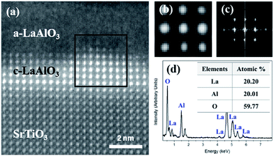
The e-beam-induced structural evolution was elucidated from a cross-sectional specimen using Cs-corrected STEM. Fig. 1a shows a high-angle annular dark field (HAADF) STEM image of as-grown a-LAO/STO along the [100] zone axis after e-beam irradiation by continuously scanning the entire area shown with a e-beam current of 0.34 nA. The incident e-beam for imaging and irradiation both is perpendicular to the TEM specimen of [100] crystal orientation. Before irradiation, only the a-LAO overlayer with no crystal lattice features was observed on the perovskite STO substrate; however, after e-beam irradiation, a newly formed crystal layer with a bright contrast grew epitaxially from the interface. The bright contrast of the new crystal indicates that it is a La-containing phase since the intensity of an atomic column is approximately proportional to the atomic number Z2 in the HAADF STEM image.36,37 Owing to the high intensity of the A-cation-site column, the atomic column of a B-cation site is not visible in Fig. 1a, but the filtered atomic-column image in Fig. 1b clearly shows that a B cation is located at the center of the A-cation unit cell. In addition, a fast Fourier transform (FFT) of the diffraction pattern of the boxed crystallized region in Fig. 1a (Fig. 1c) indicates that the new crystal has a pseudocubic structure with a lattice parameter of 3.8 Å. The quantitative ratio of La![[thin space (1/6-em)]](https://www.rsc.org/images/entities/char_2009.gif) :
:![[thin space (1/6-em)]](https://www.rsc.org/images/entities/char_2009.gif) Al
Al![[thin space (1/6-em)]](https://www.rsc.org/images/entities/char_2009.gif) :
:![[thin space (1/6-em)]](https://www.rsc.org/images/entities/char_2009.gif) O as 1
O as 1![[thin space (1/6-em)]](https://www.rsc.org/images/entities/char_2009.gif) :
:![[thin space (1/6-em)]](https://www.rsc.org/images/entities/char_2009.gif) 1
1![[thin space (1/6-em)]](https://www.rsc.org/images/entities/char_2009.gif) :
:![[thin space (1/6-em)]](https://www.rsc.org/images/entities/char_2009.gif) 3 was estimated from a chemical composition analysis obtained by energy-dispersive X-ray spectroscopy (EDS) (Fig. 1d). The analyses of the crystal structure and chemical composition revealed that the crystallized LAO is perovskite-type pseudocubic LaAlO3. The reference atomic structure of crystalline LAO (c-LAO) grown on the STO substrate during the pulsed laser deposition (PLD) process can be found in a previous report.38
3 was estimated from a chemical composition analysis obtained by energy-dispersive X-ray spectroscopy (EDS) (Fig. 1d). The analyses of the crystal structure and chemical composition revealed that the crystallized LAO is perovskite-type pseudocubic LaAlO3. The reference atomic structure of crystalline LAO (c-LAO) grown on the STO substrate during the pulsed laser deposition (PLD) process can be found in a previous report.38
Critical e-beam distance from the heterointerface for the epitaxial crystallization of a-LAO
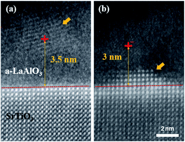
Regarding the origin of the epitaxial crystallization, the beam-position effect was systematically investigated, as shown in Fig. 2. The specimens were irradiated by a focused beam at an electron dose rate of 0.169 × 10⁹ e− Å−1 s−1 and a e-beam current of 0.34 nA. When the convergent e-beam was positioned on the a-LAO overlayer at a distance of 3.5 nm from the interface for 60 s, randomly oriented local crystallization occurred (Fig. 2a). In addition, epitaxial crystal growth occurred from the interface when the beam was positioned within 3 nm from the a-LAO/STO heterointerface (Fig. 2b). After 60 s of irradiation, four new atomic layers grew from the initial interface (red dashed line) in a pyramidal shape. This result implies that the e-beam-induced crystal quality, i.e., an epitaxially grown single crystal or a randomly oriented polycrystal, can be controlled by the beam distance from the interface between the amorphous and crystalline phases. This also means that the beam does not need to irradiate the crystal substrate directly to obtain epitaxial growth; instead, an e-beam located at some short distance can activate the interface region in this material. Note that crystallization was initiated from the interface rather than the directly irradiated beam position when it was within a critical distance—3 nm in this sample. The diameter of the convergent beam should theoretically be smaller than 0.2 nm in the STEM mode, and the distance between the e-beam and the interface was 3 nm, which is sufficiently large compared to the probe size. Beam delocalization also should be considered but would not be as large as 3 nm in the thin-foil TEM sample. Therefore, e-beam-induced direct atomic rearrangement might not be the major reason for crystal growth. The crystal growth at the heterointerface rather than the nucleation at the beam position within a critical distance indicates that the required activation energy for epitaxial and heterogeneous crystal growth at the interface is lower than the homogeneous nucleation energy in a-LAO.Crystallization behaviors and kinetics depending on various factors
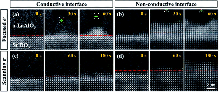
In addition to the e-beam position, factors such as the e-beam dose rate, the external field, and the atomic structure at the interface also affect the crystallization behavior.39–42 In this study, we found that a local electric field formed between the e-beam and the heterostructure interface, which determines the crystallization kinetics. The interfacial conductivity at the a-LAO/STO heterostructure interface is controllable with subsequent thermal annealing under a high oxygen pressure.35 The current at the interface of the as-grown a-LAO/STO heterostructure evaluated by current–voltage (I–V) measurements was 1.77 × 10⁻⁴ A, which was reduced to 1.24 × 10⁻¹⁰ A at 5 V after annealing at 500 °C under an oxygen pressure of 300 Torr (see Fig. S1 in the ESI†). When the interface—acting as a bottom electrode—is insulating, the electrons injected during irradiation accumulate around the beam position. However, when the interface becomes conductive and thus acts as a current path, a local field is applied between the negatively charge e-beam position and its counterpart—the relatively positive interface.Fig. 3 compares the epitaxial crystallization behavior depending on the conductivity of the interface. In Fig. 3a and b, the converged e-beam was focused at a position that was 3 nm from the heterointerface for 60 s. When the interface is conductive, epitaxial crystallization occurred, resulting in a pyramidal shape, and a crystal grew in a narrow columnar shape that followed the movement of the incident beam from the interface (Fig. 3a). This result demonstrates the possibility of nanoscale manipulation of the crystalline oxide nanostructure using a high-energy e-beam. In contrast, relatively fast and uncontrollable crystallization occurred over a wide area when the interface was not conductive after the thermal treatment (Fig. 3b). Similarly, a wide range of crystallization was observed at the nonconductive interface when the e-beam was not focused at a specific position but continuously scanned over the region of interest, i.e., the search mode with simultaneous irradiation and observation (Fig. 3c and d). Interestingly, the crystallization kinetics were obviously different depending on the interfacial conductivity. In Fig. 3c, only two new LAO unit cells grew from the dashed red line (initial state) after e-beam irradiation for 180 s. In the meantime, six new crystalline layers formed at the nonconductive interface (Fig. 3d). Therefore, a deliberate crystal pattern can be obtained at the conductive heterointerface owing to the delayed crystallization rate.
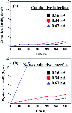
The e-beam current is another factor that determines the crystallization behaviors. The graphs in Fig. 4 demonstrate the crystallization kinetics depending on the e-beam current in a-LAO/STO with and without the 2DEG. The newly formed LAO unit cells were counted every 30 s. At the conductive interface, the crystallization rate was very slow such that no distinct discrepancy was observed after irradiation for 180 s with an e-beam current of 0.16–0.67 nA (Fig. 4a). On the other hand, the crystallization rate dramatically increased depending on the beam current in the sample with no interfacial conductivity (Fig. 4b). After 60 s of irradiation with an e-beam current of 0.67 nA, more than 20 atomic layers were grown above the nonconductive interface. A lower sensitivity to the electron dose rate at the interface with a high mobility indicates that the injected electrons quickly dissipate through the conductive interface.
The crystallization mechanism by e-beam irradiation has been explained with an enhanced defect mobility by elastic interactions, the rearrangement of unstable bonds, charge accumulation, and the heating effect.18,43–45 Among them, the local heating effect by the inelastic scattering of incident electrons with the electrons in the specimen can be considered as one of the reasons for the crystallization observed in this study. Since the energy of the incident electrons is mostly transferred to the heated specimen, an increase in the temperature of a local area can occur, which can be calculated by Egerton's equation as follows:18
I < E (eV) > (t/λ) = 4πκt(T − T0)/[0.58 + 2![[thin space (1/6-em)]](https://www.rsc.org/images/entities/char_2009.gif) ln(2R0/d)] + π(d2/2)εσ(T4 − T04) ln(2R0/d)] + π(d2/2)εσ(T4 − T04)
| (1) |
Electron charge accumulation and annihilation at the a-LAO/STO heterointerface
In addition, we provide evidence of the charge accumulation effect on the crystallization kinetics in this study. When the heterointerface is conductive, the crystallization kinetics were relatively slow; thus, deliberate manipulation was possible, which implies that the interfacial conductivity plays a significant role in determining the crystallization behavior. The schematic in Fig. 5a demonstrates that negative charges accumulate when the incident e-beam is focused at a specific position since STO and a-LAO are both insulating. Thus, the concentrated negative charges at the nonconductive interface as well as the a-LAO overlayer enhance the migration of ions, thereby facilitating crystal growth from the interface.50–53 In this case, crystallization occurs quickly at the e-beam-affected and charge-accumulated neighboring region, which is uncontrollable in size and speed. On the contrary, the conductive layer confined at the heterointerface of a-LAO/STO acts as a path for the incident electrons to flow through.35 In other words, the incident negative charges are dissipated through the conductive interface without accumulation (Fig. 5b). Therefore, crystallization occurs at a suppressed rate regardless of the e-beam current, and the resulting initial shape of the crystalline region is pyramidal with a narrow width. Combined with the scanning beam control system successfully developed by Jesse et al., an elaborate crystal pattern is expected to be created at the atomic scale using this material and irradiation conditions.9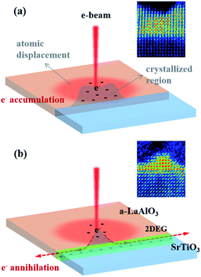 | ||
| Fig. 5 Schematics showing the distribution of electrons around the incident e-beam in the a-LAO overlayer. (a) The incident electrons accumulate when the interface is insulating. (b) The negative charges are dissipated through the conductive interface, which acts as a bottom electrode. The inset images are colored HRSTEM images of Fig. 3a and b showing the crystallization kinetics and shape. | ||
Considering the control parameters such as interfacial conductivity, dose rate and critical e-beam distance, ‘NANO’ letters patterning was successfully obtained (Fig. 6). Here, a-LAO/STO having 2DEG was used in order to control the shape and size of the pattern delicately. It shows that patterns with nanometer scale can be manipulated using e-beam irradiation, and this opens a new horizon for STEM e-beam lithography.
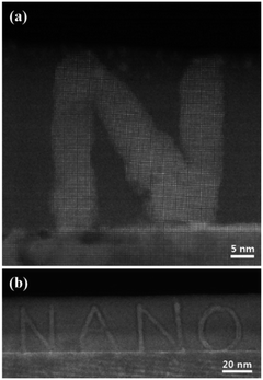 | ||
| Fig. 6 HAADF STEM images of patterned letters onto a-LAO region using e-beam irradiation. The pattern keeps the coherent atomic structure from the STO3 crystalline substrate. | ||
Conclusions
In summary, the e-beam controlled epitaxial crystallization behavior of an a-LAO thin film that has an interface with an STO substrate was investigated. The crystallization product was perovskite-type pseudocubic LaAlO3 according to the chemical and diffraction-pattern analyses. The origin of the crystallization observed in this study is elastic-scattering-induced atomic rearrangement rather than the local heating effect. When a convergent e-beam was focused at a specific position, heterogeneous nucleation occurred. However, when it was positioned within a critical distance from the interface with the substrate (3 nm in this study), epitaxial crystal growth at the heterointerface preferentially occurred. Thus, it can be noticed that the crystallization at the interface within a distance of e-beam is energetically preferred even though the interface is not directly irradiated with the e-beam. The crystallization kinetics can be controlled by the electrical conductivity of the interface and the dose rate. The 2DEG, acting as a current path for accumulated electrons, delayed the crystallization; thus, delicate manipulation of the crystal pattern at an atomic level is possible.Recently, the fabrication and manipulation of nanostructures for electronic devices has received considerable attention and created the new research field of “nanoarchitectonics”. Hence, we believe that this systematic study of the materials' electrical properties and the parameters that control the e-beam-induced crystallization will provide useful guidelines for nanoscale EBL and encourage research on the fabrication of atomically manipulated nanostructures.
Conflicts of interest
There are no conflicts to declare.Acknowledgements
The authors thank Young Woo Jeong and Min-kyung Cho at Advanced Analysis Center, KIST for important contributions in TEM sampling and STEM observation, respectively. This research was supported by Basic Science Research Program through the National Research Foundation of Korea (NRF) funded by the Ministry of Science, ICT and future Planning (2017R1A2B2012514) and the KIST Institutional Program (2V05210).Notes and references
- S. Okazaki, J. Vac. Sci. Technol., B: Microelectron. Nanometer Struct., 1991, 9, 2829–2833 CrossRef CAS.
- C. Vieu, F. Carcenac, A. Pepin, Y. Chen, M. Mejias, A. Lebib, L. Manin-Ferlazzo, L. Couraud and H. Launois, Appl. Surf. Sci., 2000, 164, 111–117 CrossRef CAS.
- A. Broers, A. Hoole and J. Ryan, Microelectron. Eng., 1996, 32, 131–142 CrossRef CAS.
- A. Heuberger, J. Vac. Sci. Technol., B: Microelectron. Process. Phenom., 1988, 6, 107–121 CAS.
- W. L. Brown, T. Venkatesan and A. Wagner, Nucl. Instrum. Methods Phys. Res., 1981, 191, 157–168 CrossRef CAS.
- Y. Chen, Microelectron. Eng., 2015, 135, 57–72 CrossRef CAS.
- M. A. Guillorn, D. W. Carr, R. C. Tiberio, E. Greenbaum and M. L. Simpson, J. Vac. Sci. Technol., B: Microelectron. Nanometer Struct., 2000, 18, 1177–1181 CrossRef CAS.
- K. Liu, P. Avouris, J. Bucchignano, R. Martel, S. Sun and J. Michl, Appl. Phys. Lett., 2002, 80, 865–867 CrossRef CAS.
- S. Jesse, Q. He, A. R. Lupini, D. N. Leonard, M. P. Oxley, O. Ovchinnikov, R. R. Unocic, A. Tselev, M. Fuentes-Cabrera and B. G. Sumpter, Small, 2015, 11, 5895–5900 CrossRef CAS PubMed.
- B. Song, G. F. Schneider, Q. Xu, G. Pandraud, C. Dekker and H. Zandbergen, Nano Lett., 2011, 11, 2247–2250 CrossRef CAS PubMed.
- Q. Xu, M.-Y. Wu, G. F. Schneider, L. Houben, S. K. Malladi, C. Dekker, E. Yucelen, R. E. Dunin-Borkowski and H. W. Zandbergen, ACS Nano, 2013, 7, 1566–1572 CrossRef CAS PubMed.
- I. Jencic, M. Bench, I. Robertson and M. Kirk, J. Appl. Phys., 1995, 78, 974–982 CrossRef CAS.
- S. Watanabe, Mater. Sci. Forum, 2007, 561, 2021–2024 CrossRef.
- F. Lu, Z. Dong, J. Zhang, T. White, R. C. Ewing and J. Lian, RSC Adv., 2013, 3, 15178–15184 RSC.
- W. Clark, J. Chapman, A. Macleod and R. Ferrier, Ultramicroscopy, 1980, 5, 195–208 CrossRef CAS.
- H. J. Park, G. H. Ryu and Z. Lee, Applied Microscopy, 2015, 45, 107–114 CrossRef.
- D. B. Williams and C. B. Carter, Transmission Electron Microscopy: A Text Book for Materials Science, Springer, New York, 2009, p. 64 Search PubMed.
- R. Egerton, P. Li and M. Malac, Micron, 2004, 35, 399–409 CrossRef CAS PubMed.
- L. Yao, S. Majumdar, L. Äkäslompolo, S. Inkinen, Q. H. Qin and S. van Dijken, Adv. Mater., 2014, 26, 2789–2793 CrossRef CAS PubMed.
- P. I. Gaiduk, F. F. Komarov and V. S. Tishkov, Phys. Rev. B: Condens. Matter Mater. Phys., 2000, 61, 23 CrossRef.
- F. Priolo and E. Rimini, Mater. Sci. Rep., 1990, 5, 321–379 CrossRef.
- J. Parsons, R. Balluffi and J. Koehler, Appl. Phys. Lett., 1962, 1, 57–58 CrossRef CAS.
- K. Naoto, H. Masataka, K. Hisao, H. Nobuyuki, S. Makoto, O. Fumihiko and A. Masatoshi, Nucl. Instrum. Methods Phys. Res., Sect. B, 1991, 59, 449–453 CrossRef.
- K. Ariga, Q. Ji, W. Nakanishi, J. P. Hill and M. Aono, Mater. Horiz., 2015, 2, 406–413 RSC.
- Z. Liu, Y.-C. Lin, C.-C. Lu, C.-H. Yeh, P.-W. Chiu, S. Iijima and K. Suenaga, Nat. Commun., 2014, 5, 4055 CAS.
- A. Ohtomo and H. Hwang, Nature, 2004, 427, 423–426 CrossRef CAS PubMed.
- N. Reyren, S. Thiel, A. Caviglia, L. F. Kourkoutis, G. Hammerl, C. Richter, C. Schneider, T. Kopp, A.-S. Rüetschi and D. Jaccard, Science, 2007, 317, 1196–1199 CrossRef CAS PubMed.
- X. Wang, W. Lü, A. Annadi, Z. Liu, K. Gopinadhan, S. Dhar and T. Venkatesan, Phys. Rev. B: Condens. Matter Mater. Phys., 2011, 84, 075312 CrossRef.
- G. Herranz, F. Sánchez, N. Dix, M. Scigaj and J. Fontcuberta, Sci. Rep., 2012, 2, 758 CrossRef CAS PubMed.
- Y. Kozuka, A. Tsukazaki, D. Maryenko, J. Falson, S. Akasaka, K. Nakahara, S. Nakamura, S. Awaji, K. Ueno and M. Kawasaki, Phys. Rev. B: Condens. Matter Mater. Phys., 2011, 84, 033304 CrossRef.
- H. Störmer, R. Dingle, A. Gossard, W. Wiegmann and M. Sturge, Solid State Commun., 1979, 29, 705–709 CrossRef.
- N. Bristowe, P. Littlewood and E. Artacho, Phys. Rev. B: Condens. Matter Mater. Phys., 2011, 83, 205405 CrossRef.
- Y. Chen, N. Pryds, J. E. Kleibeuker, G. Koster, J. Sun, E. Stamate, B. Shen, G. Rijnders and S. Linderoth, Nano Lett., 2011, 11, 3774–3778 CrossRef CAS PubMed.
- A. Sambri, D. Cristensen, F. Trier, Y. Chen, S. Amoruso, N. Pryds, R. Bruzzese and X. Wang, Appl. Phys. Lett., 2012, 100, 231605 CrossRef.
- S. Y. Moon, C. W. Moon, H. J. Chang, T. Kim, C.-Y. Kang, H.-J. Choi, J.-S. Kim, S.-H. Baek and H. W. Jang, Electron. Mater. Lett., 2016, 12, 243–250 CrossRef CAS.
- T. E. Microscopy, Transmission Electron Microscopy, Plenum, 1996 Search PubMed.
- E. Okunishi, I. Ishikawa, H. Sawada, F. Hosokawa, M. Hori and Y. Kondo, Microsc. Microanal., 2009, 15, 164–165 CrossRef.
- J. Lee, J. K. Choi, S. Y. Moon, J. Park, J.-S. Kim, C. S. Hwang, S.-H. Baek, J.-H. Choi and H. J. Chang, Appl. Phys. Lett., 2015, 106, 071601 CrossRef.
- G. Lulli, P. Merli and M. V. Antisari, Phys. Rev. B: Condens. Matter Mater. Phys., 1987, 36, 8038 CrossRef CAS.
- J. Jang, J. Y. Oh, S. K. Kim, Y. J. Choi, S. Y. Yoon and C. O. Kim, Nature, 1998, 395, 481–483 CrossRef CAS.
- O. Nast and A. J. Hartmann, J. Appl. Phys., 2000, 88, 716–724 CrossRef CAS.
- Y. Yoshino, K. Inoue, M. Takeuchi and K. Ohwada, Vacuum, 1998, 51, 601–607 CrossRef CAS.
- A. Bhalla, R. Guo and R. Roy, Mater. Res. Innovations, 2000, 4, 3–26 CrossRef CAS.
- W. Weber and H. Matzke, Mater. Lett., 1986, 5, 9–16 CrossRef CAS.
- R. C. Ewing and T. J. Headley, J. Nucl. Mater., 1983, 119, 102–109 CrossRef CAS.
- A. Stanimirovic, N. Balzaretti, A. Feldman and J. Graebner, J. Mater. Res., 2001, 16, 678–682 CrossRef CAS.
- X.-B. Lu, Z.-g. Liu, Y.-p. Wang, Y. Yang, X.-p. Wang, H.-w. Zhou and B.-y. Nguyen, J. Appl. Phys., 2003, 94, 1229–1234 CrossRef CAS.
- I. Jenčič and I. Robertson, J. Mater. Res., 1996, 11, 2152–2157 CrossRef.
- G. Lulli, P. G. Merli and M. Vittori Antisari, MRS Proceedings, 1988, 100, 375 CrossRef CAS.
- C. Fu and K. Ho, Phys. Rev. Lett., 1989, 63, 1617 CrossRef CAS PubMed.
- D. Vermilyea, J. Electrochem. Soc., 1957, 104, 542–546 CrossRef CAS.
- D. Vermilyea, J. Electrochem. Soc., 1955, 102, 207–214 CrossRef CAS.
- J. Wang and A. J. Davenport, Science, 1992, 255, 1416 CAS.
Footnote |
| † Electronic supplementary information (ESI) available. See DOI: 10.1039/c7ra06353a |
| This journal is © The Royal Society of Chemistry 2017 |

