 Open Access Article
Creative Commons Attribution 3.0 Unported Licence
Ion exchange-prepared NaSbSe2 nanocrystals: electronic structure and photovoltaic properties of a new solar absorber material
Belete Asefa Aragawab,
Jifeng Sunc,
David J. Singh c and
Ming-Way Lee
 *a
*a
aInstitute of Nanoscience and Department of Physics, National Chung Hsing University, Taichung 402, Taiwan. E-mail: mwl@phys.nchu.edu.tw
bDepartment of Chemistry, Bahir Dar University, P.O. Box 79, Bahir Dar, Ethiopia
cDepartment of Physics and Astronomy, University of Missouri, Columbia, MO 65211-7010, USA
First published on 25th September 2017
Abstract
We report the calculated electronic structure, syntheses and photovoltaic properties of a new ternary solar absorber material NaSbSe2. NaSbSe2 nanocrystals (NCs) have been prepared from a Na–Sb–S precursor by the solution-based Se2− anion exchange reaction. The Na–Sb–S precursor was grown on a TiO2 electrode using the successive ionic layer adsorption and reaction (SILAR) method. X-ray diffraction shows that the synthesized NaSbSe2 NCs have the same crystal structure as the NaSbS2 precursor with the diffraction angles significantly down-shifted. Energy-dispersive X-ray spectroscopy confirms the complete anion exchange and formation of the NaSbSe2 phase. First principles calculations show that the ordered NaSbSe2 structure resulting from the ion exchange synthesis is important for the performance. The NaSbSe2 NCs have an average size of ∼17 nm and a near-optimal optical band gap Eg of 1.48 eV that is lower than the NaSbS2 precursor. Liquid-junction NaSbSe2 quantum dot-sensitized solar cells (QDSSCs) were fabricated from the synthesized NaSbSe2 NCs for the first time. The best cell, prepared using the Au counter electrode and the polysulfide electrolyte, yielded an efficiency of 2.22%, a short current density of 1.31 mA cm−2, an open-circuit voltage of 0.30 V and a fill factor of 56.4% under the reduced light intensity of 10% sun. The external quantum efficiency (EQE) spectrum covers the spectral range of 300–900 nm with a maximum EQE of 75% at λ = 500 nm. The near-optimal Eg suggests that NaSbSe2 could be a potential material for solar cells. In addition, the ion exchange method can be extended to the preparation of many new metal selenide-based solar materials from their corresponding sulfides. These materials may show improved characteristics compared to samples with more disorder.
1. Introduction
Dye-sensitized solar cells (DSSCs) are emerging as a candidate for the next generation of low-cost alternatives to Si photovoltaic devices. Their benefits include solution processing, ease of fabrication, and low costs. Due to the limitations of dye absorbers on the bandwidth of light harvesting as well as synthesis of new and low-cost dyes, inorganic semiconductor quantum dot solar absorbers have acquired increasing attention. Semiconductor quantum dot-sensitized solar cells (QDSSCs), derived on the same principle of a DSSC, are more promising due to the unique properties of semiconductor quantum dot solar absorbers such as band gap tunability and high extinction coefficient.1–5 Moreover, the multiple exciton generation effect in a quantum dot could push the Shockley–Queisser theoretical efficiency limit of 31% to 44% for single band gap solar cells.6Ternary semiconductors based on metal chalcogenides have a broader range of electrical and optical properties than either the elementary or binary compounds because of the possibility of varying the constituent elements and their compositions. One of the representative ternary semiconductors – the I–V–VI2 class, where I = Cu, Ag, or alkali metals; V = Sb, Bi; and VI = S, Se, Te, have been studied for their potential applications in thermoelectrics7–10 and solar cells.11–16 Among the various I metals, the Cu-based I–V–VI2 materials, such as Cu–Bi–S, CuSbS2, have been explored as solar materials.17–21 The Ag-based materials such as AgSbS2, Ag3SbS3, and AgBiS2 have also been reported recently.11,16,22 In contrast, I–V–VI2 materials based on alkali metals have been rarely investigated despite their ease of preparation and promising solar cell performance.23 Alkali metal antimony-based ternary chalcogenides of the type AISbXVI2 (where A = Na, K, Rb and X = S, Se) had been synthesized by the direct interaction of an alkali metal with antimony and either sulphur or selenium at extremely high temperature.24–26 The cation sub-lattice of these compounds is often disordered at high temperature and may order or partially order as temperature is lowered.
Recently a member of the alkali antimony AISbXVI2 group – NaSbS2 – has been demonstrated as a potential solar material, achieving a power conversion efficiency of 3.2% under the reduced light intensity of 0.1 sun.23 First-principles calculations indicate that the particular electronic structure, which has hybridization between Sb and S p-states of NaSbS2, could provide screening and defect tolerance for carrier collection, making NaSbS2 a potential solar material.27 Replacing the S element with the heavier Se element lowers the energy gap Eg from 1.8 (NaSbS2) to 1.6 eV (NaSbSe2), as reported by Bazakutsa et al.24 based on measurements on thin film samples. The reduced Eg would lead to a broader optical absorption band, suggesting that NaSbSe2 would have better light harvesting ability than that of NaSbS2, which is a favorable property for a solar material. In addition, NaSbSe2 has a large absorption coefficient of α = 105 cm−1 at λ = 600 nm.24 The broad absorption band and large absorption coefficient suggests that NaSbSe2 could be a potential solar absorber material. Moreover, the three elements contained in NaSbSe2 are earth-abundant, low cost, nontoxic and environmentally friendly. However, there has been no report on solar cells based on NaSbSe2 so far. Thin films of NaSbSe2 had been synthesized by thermal evaporation.24 Here NaSbSe2 nanocrystals (NCs) were produced by selenide ion exchange from a successive ionic layer adsorption reaction (SILAR)-prepared Na–Sb–S precursor. First principles calculations comparing ordered and disordered cation sub-lattices show that this synthesis method is important as cation disorder reduces the optical band gap to below the useful range. Liquid-junction quantum dot-sensitized solar cells based on NaSbSe2 are demonstrated for the first time. We investigate the effects of ion exchange time and the number of SILAR cycles on the optical spectra and photovoltaic performance of NaSbSe2. We also investigate the dependence of photovoltaic parameters on the types of counter electrode. The best cell yielded an efficiency of 2.2%, a respectable efficiency for the first report of a new solar material.
2. Experimental
2.1 Materials and methods
2.2 Synthesis of NaSbSe2 and device fabrication
The Na–Sb–S precursor was directly grown on a TiO2 electrode with a single-stage SILAR process. The SILAR growth involved the following steps: first, the TiO2 electrode was dipped into a 0.1 M SbCl3 solution in ethanol for 15 s for Sb3+ ionic layer adsorption, followed by rinsing with pure ethanol and drying in air. Second, this electrode was dipped in to a 0.1 M Na2S solution in methanol for 1 min, followed by rinsing with pure methanol and drying in air. These two steps together are termed as one SILAR cycle. This process was repeated 11 times to grow 11 SILAR cycles of Na–Sb–S precursor. Meanwhile, a Se2− solution was made by dissolving 0.36 g of selenium powder and 0.3 g of NaBH4 in 125 ml of ethanol under N2 gas flow. The solution turned from black to colorless within a few minutes, showing the reduction of Se powder to Se2− ion. The Na–Sb–S precursor grown on the TiO2 electrode was dipped into this solution for the exchange of S2− in the Na–Sb–S structure by Se2− from the solution. Then NaSbSe2 nanocrystals (NCs) were obtained after annealing the material at 300 °C for 40 min under flowing N2 gas. The NaSbSe2 NCs were further coated with a ZnSe passivation layer to passivate surface defects according to the procedure described in the literature.28 The solar cells were fabricated by arranging the photoelectrode and counter electrode in a sandwich-type assembly and sealing them with a 190 μm-thick parafilm thermoplastic spacer. Pt and Au-coated FTO substrates were employed as the counter electrodes (CE). Pt CEs were made by dropping a 0.005 M H2PtCl6 ethanol solution on an FTO substrate, followed by annealing in a furnace at 400 °C for 15 min. This is below the temperature of ∼480 °C at which cation disorder is induced.24 The Au CE film, ∼70 nm in thickness, was deposited onto an FTO substrate by sputtering. The polysulfide electrolyte consisted of 0.25 M Na2S, 1 M S, 0.2 M KCl, and 0.1 M KI in a methanol/DI water (volume ratio 7![[thin space (1/6-em)]](https://www.rsc.org/images/entities/char_2009.gif) :
:![[thin space (1/6-em)]](https://www.rsc.org/images/entities/char_2009.gif) 3) solution. The electrolyte was injected separately through a predrilled hole on the counter electrode into the cell.
3) solution. The electrolyte was injected separately through a predrilled hole on the counter electrode into the cell.
2.3 Material characterization and photovoltaic measurements
The crystalline structure and phase purity of NaSbSe2 was analyzed by X-ray diffraction (XRD, Bruker, D8 SSS). Transmission electron microscope (TEM, Joel JEM-2010) was used to determine the crystal size and morphology. Optical property was studied using a Hitachi U-2800A UV-Vis spectrophotometer. The complete ion exchange and elemental analysis was confirmed by energy-dispersive X-ray spectroscopy (EDS coupled SEM, JEOL, JSM-7600F). The photovoltaic performance was studied by measuring photocurrent–voltage (I–V) curves using a Keithley 2400 source meter under 100 mW cm−2 light illumination from an Oriel 150 W Xe lamp with an Oriel band-pass filter simulating the AM 1.5 solar spectrum. External quantum efficiency (EQE) was measured using the monochromatic light generated from a 250W tungsten halogen lamp.2.4 First principles calculations
Two structural models were investigated. The first was a monoclinic structure based on the structure of NaSbS2, with S replaced by Se and fully relaxed lattice parameters and atomic positions. This model represents the experimental samples studied here. The second model is a model is a special quasirandom structure (SQS) with cation disorder. We used the reported NaCl structure lattice parameter of 5.966 Å and constructed a 16 atom supercell following the method of Wei and Zunger.29 The atomic coordinates were fully relaxed. The structure relaxations were done using the generalized gradient approximation (GGA) of Perdew, Burke and Ernzerhof (PBE).30 The full relaxation for the monoclinic structure was done using the projector augmented wave (PAW) method as implemented in the VASP code,31 with a cut-off energy of 400 eV. All other calculations were done using the linearized augmented planewave (LAPW) method as implemented in the WIEN2k code. Electronic structures and optical properties were obtained using the modified Becke–Johnson (mBJ) potential, which generally give improved band gaps compared to the PBE GGA.32,33 LAPW spheres of radius 2.3 Bohr were used for all atoms, and spin–orbit was included.3. Results and discussion
The Na–Sb–S precursor was synthesized based on the reaction between Sb2S3 and Na2S as given in eqn (1) below,34| Sb2S3 + Na2S → 2NaSbS2. | (1) |
After annealing the Na–Sb–S precursor under N2 gas, clear diffraction peaks, shown in Fig. 1 (middle panel), appearing at 16.81, 21.51, 28.60, 30.59, 31.56, 35.40, 43.83, and 45.31° all match well with the (110), (020), (![[1 with combining macron]](https://www.rsc.org/images/entities/char_0031_0304.gif) 12), (
12), (![[2 with combining macron]](https://www.rsc.org/images/entities/char_0032_0304.gif) 21), (002), (
21), (002), (![[1 with combining macron]](https://www.rsc.org/images/entities/char_0031_0304.gif) 31), (221) and (
31), (221) and (![[2 with combining macron]](https://www.rsc.org/images/entities/char_0032_0304.gif) 23) planes of the monoclinic NaSbS2 reference pattern (JCPDS No. 00-032-1039). There are no other impurity phases observed in the spectrum. The other larger peaks observed belong to either TiO2 or the FTO substrate (labeled as # in the figure).
23) planes of the monoclinic NaSbS2 reference pattern (JCPDS No. 00-032-1039). There are no other impurity phases observed in the spectrum. The other larger peaks observed belong to either TiO2 or the FTO substrate (labeled as # in the figure).
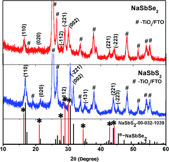 | ||
| Fig. 1 X-ray diffraction patterns of NaSbSe2 and NaSbS2 nanocrystals. Bottom panel: black lines: NaSbS2 reference pattern; red lines with * symbol: NaSbSe2 reference pattern. | ||
The pre-annealed NaSbS2 precursor was used for S2− exchange with Se2−, as demonstrated by eqn (2),
| NaSbS2 + Se2− → NaSbSe2 + S2− | (2) |
The basis of eqn (2) is explained as follows. The most important factor for driving the ion exchange reaction is the thermodynamic factor. Ions in a solid with a relatively higher solubility can be exchanged by other ions in solution if the product has a lower solubility. The solubility product (Ksp), is related to the free energy change of the process. The Ksp of metal selenides is lower than that of metal sulfide. Even though the actual solubility can be controlled by many factors, the solubility products of metal chalcogenides have a lower value as the ionic radius of chalcogen increases. That is the ion exchange of S in the crystal with Se2− is thermodynamically feasible process. Once the ion exchange is initiated on the solid–solution interface, further exchange requires the diffusion of ions towards the core of the solid. The inward selenium ion diffusion is accompanied with sulfur ion diffuse towards the solution. In addition, the time required for the exchange reaction is a function of the magnitude of the kinetic barrier for the process.
X-ray diffraction analysis of NaSbSe2 confirms the successful preparation of single-phase NaSbSe2 NCs (Fig. 2, top panel). The pronounced NaSbSe2 peaks are (110), (![[2 with combining macron]](https://www.rsc.org/images/entities/char_0032_0304.gif) 21), (002), (221), and (
21), (002), (221), and (![[2 with combining macron]](https://www.rsc.org/images/entities/char_0032_0304.gif) 23). After conversion to NaSbSe2, the crystal structure maintained the same monoclinic phase with each (hkl) peak shifted to a lower angle relative to the corresponding NaSbS2 peak. For example, the (002) plane shifted from 31.53 (NaSbS2) to 30.13 (NaSbSe2). Our first principles calculations yield lattice parameters, a = 8.433 Å, b = 7.230 Å, c = 8.716 Å, γ = 59.986°, for a volume 16% larger (∼5% linear expansion) than the sulfide, in reasonable accord with these shifts in diffraction peak position. The lower angle shifts are due to lattice expansion as a result of the replacement of smaller S2− (0.184 nm) with larger Se2− (0.198 nm). A size difference of 0.014 nm per atom produces a significant lattice expansion after a complete exchange of S2− with Se2−, which is in agreement with the significant lower angle shifts of the NaSbSe2 peaks relative to the NaSbS2 peaks. The monoclinic structure found is to be contrasted with that normally obtained by high temperature synthesis, which is NaCl with cation disorder, and partial ordering below 480 °C. The average crystallite size of the NaSbSe2 NCs, calculated using the Scherrer's equation from the dominant diffraction peak, is ∼19 nm, which is close to the size determined from the TEM image shown in Fig. 2 below.
23). After conversion to NaSbSe2, the crystal structure maintained the same monoclinic phase with each (hkl) peak shifted to a lower angle relative to the corresponding NaSbS2 peak. For example, the (002) plane shifted from 31.53 (NaSbS2) to 30.13 (NaSbSe2). Our first principles calculations yield lattice parameters, a = 8.433 Å, b = 7.230 Å, c = 8.716 Å, γ = 59.986°, for a volume 16% larger (∼5% linear expansion) than the sulfide, in reasonable accord with these shifts in diffraction peak position. The lower angle shifts are due to lattice expansion as a result of the replacement of smaller S2− (0.184 nm) with larger Se2− (0.198 nm). A size difference of 0.014 nm per atom produces a significant lattice expansion after a complete exchange of S2− with Se2−, which is in agreement with the significant lower angle shifts of the NaSbSe2 peaks relative to the NaSbS2 peaks. The monoclinic structure found is to be contrasted with that normally obtained by high temperature synthesis, which is NaCl with cation disorder, and partial ordering below 480 °C. The average crystallite size of the NaSbSe2 NCs, calculated using the Scherrer's equation from the dominant diffraction peak, is ∼19 nm, which is close to the size determined from the TEM image shown in Fig. 2 below.
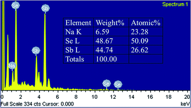
The EDS elemental analysis in Fig. 2 displays the percentage of atoms in the NaSbSe2 sample. The ratio of Na![[thin space (1/6-em)]](https://www.rsc.org/images/entities/char_2009.gif) :
:![[thin space (1/6-em)]](https://www.rsc.org/images/entities/char_2009.gif) Sb
Sb![[thin space (1/6-em)]](https://www.rsc.org/images/entities/char_2009.gif) :
:![[thin space (1/6-em)]](https://www.rsc.org/images/entities/char_2009.gif) Se is 1
Se is 1![[thin space (1/6-em)]](https://www.rsc.org/images/entities/char_2009.gif) :
:![[thin space (1/6-em)]](https://www.rsc.org/images/entities/char_2009.gif) 1.14
1.14![[thin space (1/6-em)]](https://www.rsc.org/images/entities/char_2009.gif) :
:![[thin space (1/6-em)]](https://www.rsc.org/images/entities/char_2009.gif) 2.15, in close agreement with the atomic ratio 1
2.15, in close agreement with the atomic ratio 1![[thin space (1/6-em)]](https://www.rsc.org/images/entities/char_2009.gif) :
:![[thin space (1/6-em)]](https://www.rsc.org/images/entities/char_2009.gif) 1
1![[thin space (1/6-em)]](https://www.rsc.org/images/entities/char_2009.gif) :
:![[thin space (1/6-em)]](https://www.rsc.org/images/entities/char_2009.gif) 2 of NaSbSe2. The residual amount of sulfur in the sample is undetectable, confirming the complete exchange of S with Se.
2 of NaSbSe2. The residual amount of sulfur in the sample is undetectable, confirming the complete exchange of S with Se.
The TEM images in Fig. 3 show the synthesized particles prior to and after the ion exchange reaction. Fig. 3(a) shows the NaSbS2 NCs and Fig. 3(b) shows the NaSbSe2 NCs deposited on a 30 nm TiO2 substrate. The NaSbS2 and NaSbSe2 NCs have spherical morphology and exhibit no significant changes in morphology and size after ion exchange. There is no observable aggregation during the SILAR growth of NaSbSe2 NCs. The NaSbSe2 NC size ranges from 15–18 nm, with an average diameter of 17 nm.
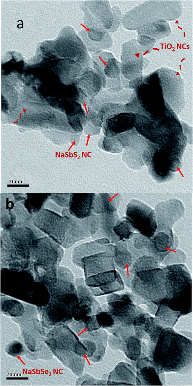 | ||
| Fig. 3 TEM images of nanocrystals deposited on the surface of TiO2: (a) NaSbS2 and (b) NaSbSe2. The red solid arrows mark the NaSbS2 or NaSbSe2 NCs while the red-dashed arrows mark TiO2 particles. | ||
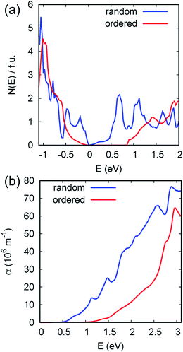
The first principles density of states and direction averaged optical absorption spectra for the ordered monoclinic structure, representing the experiments, and the disordered SQS model are contrasted in Fig. 4. As seen the electronic structure and optical spectrum are very different for these two structures. NaCl structure NaSbSe2 with full cation disorder is found to be semimetallic, with an onset of strong optical absorption at 0.5 eV. The ordered monoclinic structure has a calculated indirect band gap of 0.85 eV. The onset of direct optical absorption is at ∼1 eV with strong absorption above ∼1.5 eV, roughly in accord with the experimental data. Projections of the density of states (not shown) show substantial hybridization between the Se p orbitals making up the valence bands and the nominally unoccupied Sb p orbitals, similar to NaSbS2. This type of hybridization favors high mobility due to defect screening, as was discussed previously for NaSbS2.27
Fig. 5(a) shows the UV-visible transmission spectra T(λ) of three Na–Sb–Se samples: NaSbS2, NaSb(S/Se)2 and NaSbSe2. The three samples were prepared with different ion exchange times of 0, 15 and 40 min, respectively, which changed the crystallographic structures from NaSbS2 (0 min) to NaSb(S/Se)2 (15 min) to NaSbSe2 (40 min). The transmission edge of NaSbS2 appears at a higher energy relative to that of the NaSb(S/Se)2 and NaSbSe2 NCs (see Fig. 5(a)). After 15 minutes of S2− ion exchange reaction with Se2−, a significant redshift in transmission edge was observed. A further red shift in transmission edge was observed after 40 minutes of ion exchange. The transmission edge of NaSbSe2 (determined as the wavelength where T(λ) < 1%, i.e. absorption = 99%) is ∼757 nm, while for NaSbS2 is at a lower wavelength of 630 nm, showing that NaSbSe2 has a broader absorption range. The energy gaps Eg for NaSbS2, NaSb(S/Se)2 and NaSbSe2 NCs were determined from Tauc plots by extrapolating the curves to y = 0 as shown in Fig. 5(b). Eg decreases in the order of NaSbS2 (1.71 eV), NaSb(S/Se)2 (1.54 eV), NaSbSe2 (1.48 eV), in agreement with previous reports.23,24 NaSbSe2 NCs (1.48 eV) have the lowest Eg, resulting in a broader optical absorption range of solar spectrum. The Eg also exhibits a dependence on the particle size of NaSbSe2 NCs. Fig. 5(c) shows the Tauc plots of three NaSbSe2 NCs with different SILAR numbers. The three samples had undergone thorough ion exchange reactions and exhibited the pure NaSbSe2 phase. A lower SILAR number produces smaller-sized NaSbSe2 NCs with a higher Eg due to the quantum size effect.35 When the SILAR number is increased from 9, 10 to 11, the size of the NaSbSe2 NCs would grow larger and the Eg is lowered from 1.74, 1.60 to 1.47 eV, respectively. A notable feature is that the NaSbSe2 sample with 11 SILAR cycles has an optical Eg of 1.48 eV, which is very close to the optimal Eg of ∼1.4 eV for a solar absorber,36 suggesting that NaSbSe2 has the potential to be a highly efficient solar absorber.
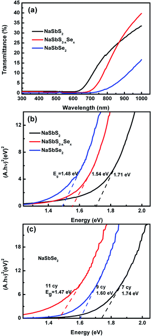 | ||
| Fig. 5 Optical spectra for NaSbS2, NaSbS2−xSex and NaSbSe2 NCs: (a) transmission and (b) (Ahν)2 vs. hν plots. (c) Eg of NaSbSe2 NCs prepared with different SILAR cycles. | ||
3.1 Photovoltaic performance
Fig. 6 shows the I–V curves of NaSbSe2 QDSSCs for various SILAR cycles n and counter electrodes under 1 sun illumination. The electrolyte used was polysulfide and the counter electrode was Pt. The photovoltaic parameters – short-circuit current density (Jsc), fill factor (FF), open-circuit voltage (Voc) and power conversion efficiency (η) are given in Table 1. The SILAR cycles n has a vital effect on the η of the cells. The η of the NaSbSe2 cells increased when n was increased from 10 to 11 and then decreased when n was further increased to 12 cycles (see Fig. 6 and Table 1, sample nos. 1–3). Therefore the optimum SILAR cycle for NaSbSe2 QDSSCs is n = 11. Surface defects are common problems in SILAR-grown NCs. They act as recombination centers for photogenerated charge carriers. Surface passivation by a layer of ZnS or ZnSe coating could reduce the density of these defect sites.37 The higher conduction band of ZnSe relative to the conduction band of NaSbSe2 and TiO2 acts as an energy barrier and prevents the recombination between the photoelectrons in a NC and holes in the polysulfide electrolyte. The efficiency of NaSbSe2 QDSSCs with ZnSe passivation improved from 0.71% (before) to 0.98% (after) (see Fig. 5(a) and Table 1, sample no. 4), an increase of 38%. The efficiency improvement is the result of combined contributions from enhanced Jsc, FF and Voc. The effect of counter electrodes (CEs) on the performance of the NaSbSe2 cells was analyzed by employing two types of CEs – Pt and Au. The cell with Au CE exhibited a higher η of 1.25% (sample no. 5), a 27% enhancement relative to Pt CE (0.98%). This is mainly a result of improved Jsc = 7.35 mA cm−2 and FF = 51.7% with Au CE relative to Pt CE (Jsc = 6.28 mA cm−2 and FF = 46.1). In a polysulfide electrolyte, a Pt CE has lower electrocatalytic activity relative to an Au CE towards reduction of the electrolyte. This is due to sulfide poisoning of the catalytic active sites of a Pt CE.38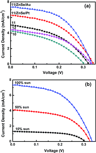 | ||
| Fig. 6 J–V curves of NaSbSe2 QDSSCs: (a) with different SILAR cycles and CEs and (b) under various reduced light intensities. CE: Au; electrolyte: polysulfide. | ||
| No | Sample | SILAR cycles n | CE | Jsc (mA cm−2) | Voc (V) | FF (%) | η (%) |
|---|---|---|---|---|---|---|---|
| 1 | NaSbSe2 | 10 | Pt | 3.79 | 0.33 | 46.1 | 0.58 |
| 2 | NaSbSe2 | 11 | Pt | 5.03 | 0.32 | 43.9 | 0.71 |
| 3 | NaSbSe2 | 12 | Pt | 4.25 | 0.30 | 41.0 | 0.52 |
| 4 | NaSbSe2/ZnSe | 11 | Pt | 6.28 | 0.34 | 46.1 | 0.98 |
| 5 | NaSbSe2/ZnSe | 11 | Au | 7.35 | 0.33 | 51.7 | 1.25 |
Fig. 6(b) displays the I–V curves of NaSbSe2 QDSSCs with Au CE under various reduced light intensities. Table 2 presents the corresponding solar cell parameters. The η increased to 2.22% as the intensity was reduced to 10% sun, a 78% increase over the 1.25% under 1 sun. Moreover, the normalized Jsc increased to 13.1 mA cm−2, which is significantly larger than Jsc = 7.35 mA cm−2 under 1 sun. The improvement in the photovoltaic performance – Jsc, FF and η – under reduced light intensities is attributed to a reduced photoelectron–hole recombination rate. The electron–hole (e–h) recombination rate is proportional to the number of e–h pairs generated by the incident light. Under a low light intensity, the absorber generates fewer charge carriers, leading to reduced recombination and improved Jsc, FF and η. The significantly improved η under low light intensities indicates that carrier recombination is an active process in the NaSbSe2 QDSSCs.
| Sun power | Jsc (mA cm−2) | Voc (V) | FF (%) | η (%) |
|---|---|---|---|---|
| 100% | 7.35 | 0.33 | 51.7 | 1.25 |
| 50% | 4.12 (8.24) | 0.32 | 53.5 | 1.41 |
| 10% | 1.31 (13.1) | 0.30 | 56.4 | 2.22 |
The efficiency (2.22%) of the present NaSbSe2 cells is lower than that (3.18%) observed in NaSbS2 cells.23 The different efficiencies are caused mainly by the different open-circuit voltage Vocs: 0.33 V in NaSbSe2 and 0.45 V in NaSbS2. Voc is proportional to the energy gap Eg. As revealed in the present work, NaSbSe2 has a smaller Eg (∼1.45 eV) than that (1.8 eV) of NaSbS2. The smaller Eg in NaSbSe2 leads to a smaller Voc and, hence, a smaller efficiency, as shown in this work. The Jsc of NaSbSe2 (7.35 mA cm−2) is smaller than that of NaSbS2 (10.76 mA cm−2). In principle, the smaller Eg in NaSbSe2 should produce a larger Jsc than that in NaSbS2 with a larger Eg. The reason for the lower Jsc is probably due to the surface defects formed on the surface of NaSbSe2 NCs during the ion-exchange reaction. The higher density of surface defects in NaSbSe2 relative to that in NaSbS2 results in a lower Jsc. With improved material growth, the problem of surface defects could be reduced and the Jsc in NaSbSe2 should eventually surpass the Jsc in NaSbS2.
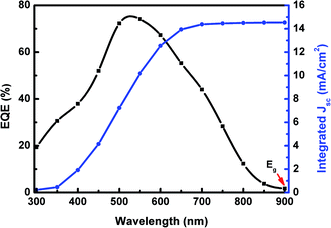
The EQE spectrum covers the spectral range from 300 to 900 nm with the maximum value of 75% at λ = 550 nm, as plotted in Fig. 7. The energy gap of NaSbSe2, determined from the onset of the EQE curve, is Eg ∼ 1.38 eV, in close agreement with the value (1.48 eV) determined from optical measurements (Fig. 5). Therefore, we conclude based on the optical and EQE data that the Eg of the material is in the range of ∼1.4–1.5 eV. The EQE integrated current density Jph, the total photocurrent that the cell can generate, can be determined from the following equation:
We summarize the notable results in this work. NaSbSe2 NCs were synthesized from the NaSbS2 precursor using the ion exchange method. The synthesized NaSbSe2 has larger lattice constants as well as a reduced optical Eg (1.48 eV) compared to that of the parent NaSbS2. This Eg is very close to the optimal Eg of a solar absorber. First principles calculations show that the synthesis method is crucial in yielded NCs with cation order and in particular that the cation disorder in material grown at high temperature will be detrimental. The best cell exhibited an efficiency of 2.2% under 0.1 sun, a respectable value for the first report of a new solar material. Since the synthesis method is a general technique, many new ternary metal selenide-based solar materials can be produced following the same technique used in this work.
4. Conclusion
In summary, we have successfully synthesized NCs from the as-synthesized Na–Sb–S precursor by the solution-phase Se2− anion exchange reaction. A reaction time of 40 min completed the NaSbS2 to NaSbSe2 exchange reaction. NaSbSe2 NCs exhibit the same crystal structure as the parent NaSbS2 precursor with larger lattice constants and a lower Eg of 1.48 eV relative to NaSbS2 (1.71 eV). The best solar cell was prepared using 11 SILAR cycles, an Au counter electrode and a ZnSe passivation coating. The best cell exhibits a normalized Jsc = 13.1 mA cm−2, a Voc = 0.30 V, a FF = 56.4% and an η = 2.22%. The near-optimal Eg suggests that NaSbSe2 has the potential to be a highly efficient solar material.Conflicts of interest
There is no conflict to declare.Acknowledgements
The authors are grateful to the financial support from the Ministry of Science and Technology of the Republic of China under grant Nos. MOST 103-2112-M-005-004-MY3 and MOST 105-2811-M-005-008. Work at the University of Missouri was supported by the U.S. Department of Energy through the S3TEC Energy Frontier Research Center, Award Number DE-SC0001299/DEFG02-09ER46577.References
- P. V. Kamat, J. Phys. Chem. C, 2008, 112, 18737–18753 CAS.
- J. Tian and G. Cao, J. Phys. Chem. Lett., 2015, 6, 1859–1869 CrossRef CAS PubMed.
- V. González-Pedro, X. Xu, I. Mora-Seró and J. Bisquert, ACS Nano, 2010, 4, 5783–5790 CrossRef PubMed.
- J. Tian, T. Shen, X. Liu, C. Fei, L. Lv and G. Cao, Sci. Rep., 2016, 6, 23094 CrossRef CAS PubMed.
- R. J. Ellingson, M. C. Beard, J. C. Johnson, P. Yu, O. I. Micic, A. J. Nozik, A. Shabaev and A. L. Efros, Nano Lett., 2005, 5, 865–871 CrossRef CAS PubMed.
- M. Green, in Third Generation Photovoltaics: Advanced Solar Energy Conversion, Springer Berlin Heidelberg, Berlin, Heidelberg, 2003, DOI:10.1007/3-540-26563-5_3, pp. 21–34.
- S. N. Guin, A. Chatterjee, D. S. Negi, R. Datta and K. Biswas, Energy Environ. Sci., 2013, 6, 2603–2608 CAS.
- S. N. Guin, V. Srihari and K. Biswas, J. Mater. Chem. A, 2015, 3, 648–655 CAS.
- S. N. Guin and K. Biswas, Chem. Mater., 2013, 25, 3225–3231 CrossRef CAS.
- C. Xiao, X. Qin, J. Zhang, R. An, J. Xu, K. Li, B. Cao, J. Yang, B. Ye and Y. Xie, J. Am. Chem. Soc., 2012, 134, 18460–18466 CrossRef CAS PubMed.
- C.-L. Chou, N. Suriyawong, B. Aragaw, J.-B. Shi and M.-W. Lee, J. Electrochem. Soc., 2016, 163, H445–H449 CrossRef CAS.
- N. Liang, W. Chen, F. Dai, X. Wu, W. Zhang, Z. Li, J. Shen, S. Huang, Q. He, J. Zai, N. Fang and X. Qian, CrystEngComm, 2015, 17, 1902–1905 RSC.
- Z. Liu, J. Huang, J. Han, T. Hong, J. Zhang and Z. Liu, Phys. Chem. Chem. Phys., 2016, 18, 16615–16620 RSC.
- M. Bernechea, N. C. Miller, G. Xercavins, D. So, A. Stavrinadis and G. Konstantatos, Nat. Photonics, 2016, 10, 521–525 CrossRef CAS.
- N. Suriyawong, B. Aragaw, J.-B. Shi and M.-W. Lee, J. Colloid Interface Sci., 2016, 473, 60–65 CrossRef CAS PubMed.
- P.-C. Huang, W.-C. Yang and M.-W. Lee, J. Phys. Chem. C, 2013, 117, 18308–18314 CAS.
- M. Kumar and C. Persson, IRESR, 2013, vol. 5, p. 031616 Search PubMed.
- K. Ramasamy, B. Tien, P. S. Archana and A. Gupta, Mater. Lett., 2014, 124, 227–230 CrossRef CAS.
- S. Dekhil, H. Dahman, S. Rabaoui, N. Yaacoub and L. El Mir, J. Mater. Sci.: Mater. Electron., 2017, 28, 11631–11635 CrossRef CAS.
- L. Wang, C. Ma, K. Hu, R. Zhou, X. Mao, S. Pan, L. H. Wong and J. Xu, J. Alloys Compd., 2016, 680, 182–190 CrossRef.
- W. Septina, S. Ikeda, Y. Iga, T. Harada and M. Matsumura, Thin Solid Films, 2014, 550, 700–704 CrossRef CAS.
- W.-C. Yang and M.-W. Lee, J. Electrochem. Soc., 2014, 161, H92–H96 CrossRef CAS.
- S. U. Rahayu, C.-L. Chou, N. Suriyawong, B. A. Aragaw, J.-B. Shi and M.-W. Lee, APL Mater., 2016, 4, 116103 CrossRef.
- V. A. Bazakutsa, N. I. Gnidash, A. K. Kul'chitskaya and A. V. Salov, Phys. Usp., 1975, 18, 472–475 Search PubMed.
- M. D. Nielsen, V. Ozolins and J. P. Heremans, Energy Environ. Sci., 2013, 6, 570–578 CAS.
- S. I. Berul', Y. G. Finkel'shtein and N. P. Luzhnaya, in Chemical Bonds in Solids: Semiconductor Crystals, Glasses, and Liquids, ed. A. N. N. Sirota, Springer US, Boston, MA, 1995, vol. 4, DOI:10.1007/978-1-4684-8682-7_28, pp. 149–154.
- J. Sun and D. J. Singh, Phys. Rev. Appl., 2017, 7, 024015 CrossRef.
- F. Huang, J. Hou, Q. Zhang, Y. Wang, R. C. Massé, S. Peng, H. Wang, J. Liu and G. Cao, Nano Energy, 2016, 26, 114–122 CrossRef CAS.
- S. H. Wei and A. Zunger, Disorder Effects on the Density of States of the II-VI Semiconductor Alloys Hg0.5Cd0.5Te, Cd0.5Zn0.5Te and Hg0.5Zn0.5Te, Phys. Rev. B: Condens. Matter Mater. Phys., 1991, 43, 14272 CrossRef CAS.
- J. P. Perdew, K. Burke and M. Ernzerhof, Generalized Gradient Approximation Made Simple, Phys. Rev. Lett., 1996, 77, 3865 CrossRef CAS PubMed.
- G. Kresse and D. Joubert, From Ultrasoft Pseudopotentials to the Projector Augmented-Wave Method, Phys. Rev. B: Condens. Matter Mater. Phys., 1999, 59, 1758 CrossRef CAS.
- F. Tran and P. Blaha, Accurate Band Gaps of Semiconductors and Insulators with a Semilocal Exchange–Correlation Potential, Phys. Rev. Lett., 2009, 102, 226401 CrossRef PubMed.
- D. J. Singh, Electronic Structure Calculations with the Tran-Blaha Modified Becke-Johnson Density Functional, Phys. Rev. B: Condens. Matter Mater. Phys., 2010, 82, 205102 CrossRef.
- C. A. Jacobson, E. C. Weaver and C. A. Hampel, Encyclopedia of chemical reactions, Reinhold Pub. Corp., New York, 1946 Search PubMed.
- S. Gorer and G. Hodes, J. Phys. Chem., 1994, 98, 5338–5346 CrossRef CAS.
- T. Zdanowicz, T. Rodziewicz and M. Zabkowska-Waclawek, Sol. Energy Mater. Sol. Cells, 2005, 87, 757–769 CrossRef CAS.
- F. Huang, Q. Zhang, B. Xu, J. Hou, Y. Wang, R. C. Masse, S. Peng, J. Liu and G. Cao, J. Mater. Chem. A, 2016, 4, 14773–14780 CAS.
- G. Hodes, J. Manassen and D. Cahen, J. Electrochem. Soc., 1980, 127, 544–549 CrossRef CAS.
| This journal is © The Royal Society of Chemistry 2017 |

