 Open Access Article
Creative Commons Attribution 3.0 Unported Licence
Mechanisms of subsurface damage and material removal during high speed grinding processes in Ni/Cu multilayers using a molecular dynamics study
QiHong Fang,
Qiong Wang ,
Jia Li*,
Xin Zeng and
YouWen Liu
State Key Laboratory of Advanced Design and Manufacturing for Vehicle Body, Hunan University, Changsha, Hunan Province 410082, PR China. E-mail: lijia123@hnu.edu.cn
First published on 30th August 2017
Abstract
The molecular dynamics (MD) simulation of Ni/Cu multilayers under a high speed grinding process with a diamond tip is performed, with the aim of investigating the effects of varying machining parameters on subsurface damage and material removal in the Ni/Cu multilayers. A series of key factors, consisting of grinding speed, tool radius and depth of cut, that influence the deformation of the workpiece are systemically studied in terms of surface morphology, dislocation movement, grinding temperature and average grinding force. Both the grinding temperature and force increase with increasing grinding speed, tool radius and depth of cut. In addition, a relatively small grinding velocity results in more stacking faults (SF) and a greater volume of material pileups on the sides of the groove. A good surface integrity of the Ni/Cu multilayers, with relatively fewer lattice defects, is more easily obtained by a machining process with a smaller tool radius or cutting depth. The results also show that the grinding temperature of Ni/Cu multilayers with varying grinding speeds, tool radii and cutting depths is higher than that of pure Ni thin film.
1. Introduction
Nanoscale machining processes in multilayers have attracted extensive research interest in recent years and have been demonstrated to offer great potential for broad applications in magnetic media, the aerospace field, micro-electro-mechanical systems (MEMS) and nano-electro-mechanical systems (NEMS).1–5 Nanoscale multilayer materials offer superior strength, strong hardness, high ductility and good morphological stability.6–9 Nevertheless, it is challenging to understand the deformation mechanism of the multilayers and further improve the machining properties of NEMS. This is because the processes of ultra-precision machining, with a length scale of only a few nanometers or less, are so difficult to observe experimentally. However, the above processes can be made visible by a molecular dynamics (MD) simulation.10–12 At the same time, it is also essential to identify the defect structure efficiently in a given atomistic configuration.13,14MD simulation has been conducted for the investigation of ultra-precision multilayer machining processes in the past few years. Guo et al.15 studied the thermal effect on the process of nanoscale material removal. Weng et al.16,17 analyzed the strengthening effect of a twin interface and the evolution of crystal defects in Ni/Cu multilayers via MD simulation. Cao et al.18 explored the effect of a semi-coherent interface on the mechanical and tribological properties of Ni–Al multilayers by using the MD method. Fang et al.19 investigated the indentation mechanical properties of Al/Ni multilayer films with different temperatures, hold times and applied loads on the structure. Cheng et al.20 solved the effect of a misfit dislocation network on the movement of dislocations in Ni/Cu multilayers with MD simulation. Moreover, Li et al.21–23 explored the subsurface damage mechanism of single crystal silicon subjected to a high grinding speed, and a model was built to predict the occurrence of dislocations.
The previous research work contributes to our understanding of dislocation evolution, interface effects and mechanical properties in multilayers. Simultaneously, the mechanisms of material removal in Ni/Cu multilayers are helpful for further understanding. Here, our work studies the surface integrity of Ni/Cu multilayers by analyzing the deformed structure and dislocation movement considering different machining parameters. In addition, the effects of grinding speed, tool radius and cutting depth on the subsurface damage mechanism are revealed in Ni/Cu multilayers.
2. Simulation method
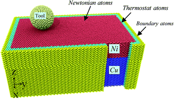
The 3D schematic of Ni/Cu multilayers is shown in Fig. 1; the MD simulation model consists of a Cu substrate, Ni thin film and a rigid diamond tip. Table 1 shows the computational parameters utilized in our MD simulations. The Cu substrate with a crystallography configuration of X – [0 3 −1], Y – [0 1 3] and Z − [1 0 0] has a size of 14 × 22 × 6 nm3 along the X, Y and Z directions, respectively, and contains 160, 327 atoms. The Ni thin film is bonded to the Cu substrate in an epitaxial mode in the current simulations. The Ni thin film, with a layer thickness of 3.0 nm, has a crystallography configuration of X − [0 3 1], Y − [0 −1 3] and Z − [1 0 0], and contains 84, 301 atoms. In order to reveal the interface effect on subsurface damage and material removal in Ni/Cu multilayers caused by a high speed grinding process, a pure single crystal Ni thin film with the same size as the Ni/Cu multilayers is also constructed. The tool tip is treated as a rigid body in a rational assumption, since diamond is much harder than either pure Ni thin film or Ni/Cu multilayers.18,22 Both X and Y directions are free surfaces in our simulations. The workpiece consists of three kinds of atoms: boundary atoms, thermostat atoms and newtonian atoms. The initial temperature of the workpiece is 293 K. The boundary atom layer (colored yellow in Fig. 1) is kept fixed, and has a thickness of 0.5 nm to support the whole system and restrict the rigid body movement of the workpiece.23,24 The thermostat atoms, with a thickness of 0.5 nm, dominate the heat dissipation of the Ni/Cu multilayers and maintain the grinding temperature at the constant 293 K by utilizing the velocity rescaling method once every five computational time steps during the MD simulation process. The motions of the thermostat atoms and newtonian atoms obey the classical second Newton's law by using the velocity-Verlet algorithm method.25| Materials | Workpiece: Ni thin film and Ni/Cu multilayers | Tool: diamond |
|---|---|---|
| Dimensions | 14 nm × 22 nm × 9 nm | Radii 2.0, 3.0, 4.0 and 5.0 nm |
| Time step | 1 fs | |
| Initial temperature | 293 K | |
| Grinding velocity (v) | 30, 50, 100, 150, and 200 m s−1 | |
| Grinding depth (h) | 0.5, 1.0, 2.0, and 2.5 nm | |
| Grinding distance (l) | 0–10 nm | |
| Grinding direction | [0 1 0] on (0 0 1) surface |
The diamond tips/tools created from perfect diamond atomic lattices have spherical shapes with radii of 2.0 nm, 3.0 nm, 4.0 nm and 5.0 nm. Each tool is treated as a rigid body because the diamond is much harder than the substrate Ni or Cu. The diamond spherical tool is modeled by a strong repulsive potential, which has been used in previous studies.26,27 The diamond tool in our simulation is spherical since the grinding tip could be simplified as a single grain in real simulation processes.
There are five different atomic interactions in the Ni/Cu multilayer MD simulation: (1) the interaction between diamond atoms (C–C) in the tool, which could be ignored since the tool tip is treated as a rigid body in the current investigation.28 (2) The interaction between the tool and the workpiece (C–Ni) atoms, which is expressed by the Morse potential,9,14,28 and could be calculated from  where E is a pair potential energy function, D0is the cohesion energy, αis the elastic modulus, and r and r0 are the instantaneous and equilibrium distances, respectively, between atoms i and j. In our simulations, the parameters of C–Ni are taken as follows: cohesion energy D = 0.1 eV, elastic modulus a = 2.2 Å−1 and equilibrium distance between two atoms r0 = 2.4 Å. The cut-off radius of the Morse potential is chosen to be 0.9025 nm in order to guarantee computational efficiency. All the above parameters are chosen according to a study by Lin et al.29 With this method, Lin et al. combined 3D MD with a finite deformation model of nano-scale cutting, to calculate the stress and strain of a single crystal nickel material in various axis directions (3, 4, 5). The interactions between atoms in the workpiece: Ni–Ni, Cu–Ni and Cu–Cu, which can be depicted by the distinguished embedded-atom method (EAM) to determine the interatomic potential of the Ni/Cu multilayers.30–32
In this study, the classical molecular dynamics package IMD33 with the time step of 1 fs is utilized in all MD simulations. The OVITO34 software is used for visualizing the MD data and generating the MD snapshots, during which the color coding command is selected to show the surface morphologies during the machining process. The common neighbor analysis (CNA) command is also chosen to show the instantaneous deformed structures and identify the feature of each atom.
3. Results and discussion
Our simulation process consists of three stages: the relaxation stage, the indention stage and the grinding stage. Atoms in the system are allowed to relax to their equilibrium configurations by using the following procedures: the atoms in the workpiece are first relaxed to their minimum energy configurations by using the famous fast inertia relaxation engine algorithm. Then the workpiece is heated up to 293 K using the Nose–Hoover thermostat for 100 ps under the isothermal–isobaric NPT ensemble.35 The purposes of the relaxation stage are to release internal stress as well as to adjust the surface tension. After full relaxation, the indentation process is carried out by moving the tip vertically towards the surface of the pure Ni thin film or Ni/Cu multilayers at a constant speed of 100 m s−1 until the desired cutting depth is reached. This is followed by the grinding process which is performed by moving the tip along the [0 1 0] direction on the (0 0 1) surface of the workpiece. In this work, we investigate the subsurface damage and material removal of the Ni/Cu multilayers when subjected to different machining methods such as tool speed, tool radius and depth of cut.3.1. Effect of tool speed
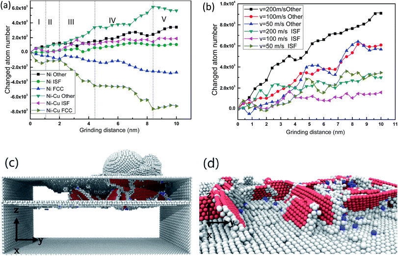
In accordance with the classification of different grinding speeds, there are three categories used to depict the speed of nanoscale machining: a general grinding speed which is less than 45 m s−1, a high grinding speed of 45–150 m s−1, and an ultra-high grinding speed which is more than 150 m s−1. In order to investigate the effect of tool speed on the deformation mechanisms of Ni/Cu multilayers during grinding processes, five grinding speeds are selected, namely 30, 50, 100, 150 and 200 m s−1.Fig. 2 exhibits the instantaneous deformed structures of Ni/Cu multilayers. Fig. 2(a) presents the evolution of different kinds of atoms in pure Ni thin film and Ni/Cu multilayers at a grinding speed of 100 m s−1, and Fig. 2(b) presents the evolution of different kinds of atoms in Ni/Cu multilayers at different grinding speeds. Fig. 2(c) and (d) show the deformed structures in Ni/Cu multilayers. As shown in Fig. 2(a), the changed atom numbers for the Ni/Cu multilayers are greater than those for pure Ni thin film. It can be seen that the plastic deformation of Ni/Cu multilayers is more serious than that of pure Ni thin film. Zone I in Fig. 2(a) shows that the curves of changed atom number fluctuate slightly and irregularly, because a few dislocation events occur when the samples are first subjected to the nanoindentation process, and over time, the dislocations formed in the plastic deformation process release energy by means of gliding.36,37 The three curves of Ni/Cu multilayers remain stable in zone II, during which successive dislocations emitted from the tool–workpiece interaction zone are absorbed by the interface in the Ni/Cu multilayers.14 The following sections (zones III, IV, V) of Ni/Cu multilayers show that the number of intrinsic stacking fault (ISF) atoms increases with the decreasing number of FCC atoms, indicating that nucleation and gliding of lattice dislocations dominate the plastic deformation; these ISF atoms turn solid and rapidly emerge at the surface and then reinforce grains as the diamond tip advances. It can be distinctly observed in Fig. 2(c) that a large number of dislocations nucleate in the Ni layer, and cannot be absorbed entirely by the interface in the Ni/Cu multilayers. As grinding proceeds, the chipping volume both in front of the grinding tip and at two sides of the grinding direction increases. The dislocation area is pushed forward by the grinding tip. Stacking faults (SFs) are shown in Fig. 2(d) at the grinding distance of 9 nm, illustrating that the interface in the Ni/Cu multilayers can serve as a valid barrier to the motion of dislocations. Due to the slipping mechanism of SFs, the internal stress can be released and in turn lead to greater strength in the multilayers. As shown in Fig. 2(b) the number of ‘other atoms’ in Ni/Cu multilayers increases quickly with grinding speed while the increase in ISF atoms is still relatively flat. This may be ascribed to the fact that there is a shorter time for the dislocations to initiate and nucleate in an orderly way when the sample is subjected to a higher grinding speed. In other words, more dislocation cores can come into being because there is little time for the atom lattices beneath the tool tip to rearrange when the grinding speed is higher.
Fig. 3(a–j) exhibits the surface morphologies of pure Ni thin film and Ni/Cu multilayers when subjected to varying grinding speeds. For the purpose of revealing the surface pileups, the atoms are colored in accordance with their heights out of the original surface. It is apparent that the volume of the surface pileups expands with increasing grinding velocity. It is known that the increasing grinding distance results in the formation of atom accumulations, thus crystal defects induce dislocation cores. These atoms spring up on the surface and thus grow into grinding chips. There is a process of recrystallization,38–41 during which lots of dislocations nucleate and glide freely on the (1 1 1) slip planes.3 Fig. 3 shows that the chipping volume on the surface of Ni/Cu multilayers is greater than that on pure Ni thin film at the same grinding speed. Fig. 3(f–j) shows that the distribution of pileups on the surface of Ni/Cu multilayers can be strongly affected by the grinding speed. By comparing Fig. 3 parts (f–j), one can see that the volume of material pileups on the sides of the groove decreases with increasing grinding speed, but that the chipping volume in front of the tool tip increases first and then decreases. It can also be found that the chipping volume in front of the grinding tip reaches a critical state at the speed of 100 m s−1. From the above, it can be found that grinding speed plays a crucial role in the surface morphologies of the Ni/Cu multilayers.
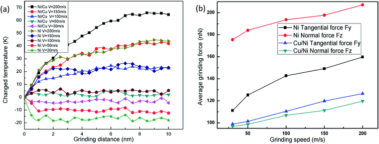
Fig. 4(a) displays the temperature change versus grinding distance in pure Ni thin film and Ni/Cu multilayers, during which the cutting depth is fixed at 2 nm. It can be seen that the grinding temperature basically remains unchanged at low grinding speeds since the wide distribution of thermostat atoms can accelerate the heat dissipation of the system when it is subjected to the grinding process. In the case of a high or ultra-high grinding speed, the grinding temperature rises with the advancement of the tool tip, and a larger grinding speed results in a greater increment in grinding temperature. Since the dislocations pile up with a higher grinding speed, the friction and extrusion between atoms become more intensive along with the motion of dislocations activated by the grinding force. At the same time, the deformed crystal lattice can release much of the friction and strain energy, and immediately transform it to the grinding heat. Thus, a higher grinding velocity inevitably results in higher grinding forces and more thermal energy. Then the curves become smooth, because the many thermostat atoms play an important role in transferring grinding heat and taking away some heat from the grinding tip during the stable grinding process. When the grinding speed remains the same, the increment in temperature in Ni/Cu multilayers is more pronounced than that in pure Ni thin film, and the curves of the Ni thin film reach a steady state earlier when compared to the Ni/Cu multilayers.
Fig. 4(b) shows the relationship between the average grinding force and grinding speed in pure Ni thin film and Ni/Cu multilayers. With increasing grinding speed, both the normal force and the tangential force increase. When the grinding speed is lower than the spread speed of a plastic wave, many of the dislocations nucleate easily, and then spread into the dislocation network. Thus the materials are strengthened and give rise to the grinding force. It can be found that the average grinding forces of pure Ni thin film are larger than those of Ni/Cu multilayers, for maintaining a high grinding speed and moving the atoms in front of the grinding tip.
3.2. Effect of tool radius
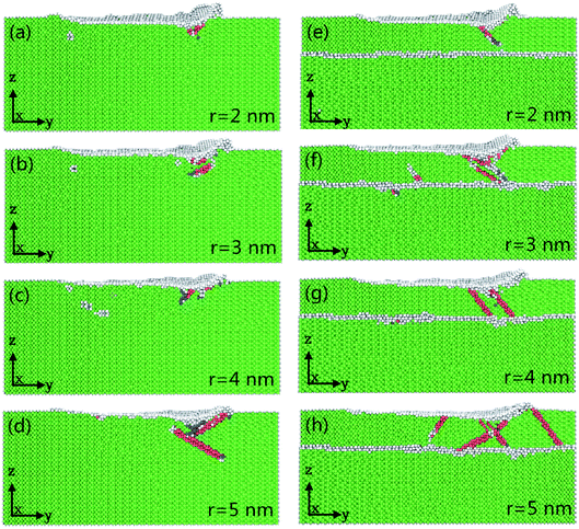
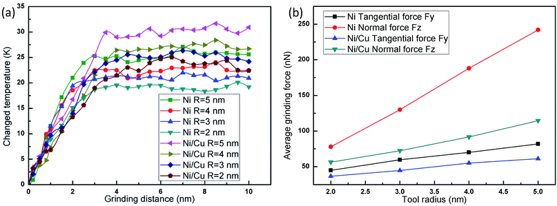
Fig. 5(a–h) shows the instantaneous deformed structures in pure Ni thin film and Ni/Cu multilayers as a result of grinding with different tool radii; atoms are colored on the basis of the calculated CNA values. It can be seen that the number of ISF atoms increases with increasing tool radius, and that more dislocations nucleate and move away from the grinding regions. It can be found that the atomic lattice distortion becomes more serious as the tool radius increases and therefore the surface properties are dramatically improved with a smaller tool radius. The tool radius plays a crucial role in the nanoscale grinding process of multilayers. When the grinding tool radius remains the same, the increment in the number of deformed structures of Ni/Cu multilayers is more serious than that of pure Ni thin film.Fig. 6(a) shows the relationship between the change in grinding temperature and grinding distance; the depth of cut and tool speed are fixed at 1 nm and 100 m s−1, respectively. It can be seen that the grinding temperature rises sharply at first and then reaches a steady value with the advancement of the tool tip. This is because the thermal conductivity of pure Ni thin film and Ni/Cu multilayers is relatively high, and so lots of thermostat atoms play an important role in the rapid transfer of grinding heat. It can be found that a larger tool radius results in a higher increment in temperature in pure Ni thin film and Ni/Cu multilayers. The larger tool radius produces more grinding heat and leads to thermal activation,42 thus energy barriers get lower and this makes it easier for dislocations to occur, as shown in Fig. 5. It can also be found that the increment in grinding temperature in Ni/Cu multilayers is more pronounced than that in pure Ni thin film at the same tool radius. Fig. 6(b) shows the relationship between average grinding force and tool radius, revealing that the increment in tool radius results in increases in both normal and tangential grinding forces in pure Ni thin film and Ni/Cu multilayers. Compared with the tangential grinding force, the increment in the normal grinding force is more pronounced. In other words, a larger grinding radius results in a larger tool–workpiece interaction zone, and a larger normal grinding force is required to maintain the high grinding speed. It can also be found that both normal and tangential grinding forces in pure Ni thin film are much bigger than those in Ni/Cu multilayers.
3.3. Effect of depth of cut
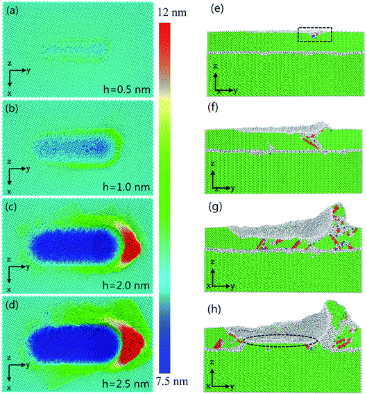
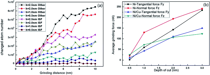
Fig. 7 shows the relationship between instantaneous deformed structures in Ni/Cu multilayers and different cutting depths, when the tool radius and grinding speed are fixed at 3 nm and 100 m s−1, respectively. Fig. 7(a–d) shows the surface morphologies with various cutting depths, in which atoms are colored in accordance with their heights out of the original surface. Fig. 7(e–h) are the Y–Z plane cross-section snapshots, in which atoms are colored in accordance with their calculated CNA values at the corresponding depth of cut. As shown in Fig. 7(a–d), it can be found that the chipping volume on the sides of the groove increases with increasing cutting depth, and the volume of the material pileups in front of the tool tip also increases. This is because a relatively larger depth of cut accelerates more atoms around the tool tip, resulting in more chipping volume. Fig. 7(e–h) shows that when the cutting depth is lower than 1.0 nm, there are few dislocations nucleated in the region of the tool tip (see the rectangle part in Fig. 7(e)). With increasing cutting depth, there are more lattice defects and greater dislocation nucleation as the tool tip moves. In the case of a cutting depth of 2.5 nm, the atomic lattice distortion becomes so serious that the interface migrates as the tool advances (see the ellipse part in Fig. 7(h)). Owing to the existence of an external stress field beneath the grinding tip, the arrangement of Ni atoms in the tool–workpiece interaction zone changes dramatically. As grinding proceeds, the plastic deformation is dominated by partial dislocations nucleated from the free surface. Then, these partial dislocations slip along their constant slip planes {111}. Hence, the dislocation structure with the cross-section view along the vertical x-axis direction may form a straight line, as shown in Fig. 5 and 7. The combination of Fig. 2(c) and (d), 5 and 7 contributes to our comprehension of the instantaneous deformed structures.Fig. 8(a) displays the changed atom number in Ni/Cu multilayers at different cutting depths. It can be seen that the deepening of cut causes an increase in both ISF and ‘other atom’ numbers. This is because a larger cutting depth results in a greater chipping volume and more dislocations as the tool advances. It can be seen that the increase in both other and ISF atom numbers in the cutting depth range from 1.0 nm to 2.0 nm is greater than that in the cutting depth range from 0.5 nm to 1.0 nm, or from 2.0 nm to 2.5 nm. Fig. 8(b) shows the curves of average grinding force versus depth of cut. It can be seen that both tangential and normal grinding forces increase with increasing cutting depth. With increasing cutting depth, more lattice defects and SFs occur in the tool–workpiece interaction zone. Fig. 8(b) also shows that the increase in tangential grinding force is more pronounced than that in the normal grinding force in Ni/Cu multilayers. This is because a larger cutting depth at the same grinding distance results in the acceleration of a larger region of atoms, and the glide of dislocations results in the dramatic increase of the tangential force. It can also be found that the increases in both the normal and the tangential grinding forces of pure Ni thin film are bigger than those of Ni/Cu multilayers.
4. Conclusion
In summary, the effects of different machining parameters on the subsurface damage and material removal behavior caused by a nanoscale high speed grinding process in pure Ni thin film and Ni/Cu multilayers are clarified by utilizing MD simulation. For the purpose of maintaining better surface integrity, consideration needs to be given to three machining parameters (grinding speed, tool radius and depth of cut) as discussed below:(1) The selection of grinding speed is vital to the grinding process in the current investigation. In Ni/Cu multilayers, a higher grinding speed increases the machining efficiency by generating more chipping volume, and simultaneously, because a larger grinding force is required to maintain the high speed, a higher grinding temperature results which further influences the propagation of dislocations. With increasing grinding speed, the above effects reach a critical state. At a constant grinding speed, the grinding temperature of the Ni/Cu multilayers is larger than that of pure Ni thin film.
(2) Comparing different tool radii with the same grinding distance in Ni/Cu multilayers, a smaller tool radius improves the quality of the ground surface by lowering the grinding heat, and reducing damaged structures by decreasing the number of ISFs. This enhances the grinding efficiency.
(3) The depth of the cut plays a significant role in the nanoscale grinding process of Ni/Cu multilayers. A high speed grinding process with a smaller cutting depth leads more easily to low subsurface damage, since fewer lattice defects and dislocations take place compared with a larger cutting depth.
Conflicts of interest
There are no conflicts to declare.Acknowledgements
The authors deeply appreciate the support from the NNSFC (11572118 and 11372103), the Hunan Provincial Science Fund for Distinguished Young Scholars (2015JJ1006), the Project of Innovation-driven Plan in Central South University of China (2015CX004), the State Key Laboratory of Powder Metallurgy, and the National Key Research and Development Program of China (2016YFB0700300).References
- B. Zhang, X. L. Zheng, H. Tokura and M. Yoshikawa, J. Mater. Process. Technol., 2003, 132, 353–364 CrossRef CAS.
- Y. H. Chang, Y. D. Shen, D. B. Kong, J. Ning, Z. C. Xiao, J. X. Liang and L. J. Zhi, RSC Adv., 2017, 7, 2544–2549 RSC.
- I. Salehinia, J. Wang, D. F. Bahr and H. M. Zbib, Int. J. Plast., 2014, 59, 119–132 CrossRef CAS.
- Y. Zeng, A. Hunter, I. J. Beyerlein and M. Koslowski, Int. J. Plast., 2016, 79, 293–313 CrossRef.
- Y. Cheng, S. Y. Zhang, J. Li, J. Sun, J. J. Wang, C. X. Qin and L. Dai, RSC Adv., 2017, 7, 21953–21961 RSC.
- Y. Liu, D. Bufford, H. Wang, C. Sun and X. Zhang, Acta Mater., 2011, 59, 1924–1933 CrossRef CAS.
- K. Mylvaganam and L. C. Zhang, Scr. Mater., 2011, 65, 214–216 CrossRef CAS.
- Y. T. Zhu, X. Z. Liao and X. L. Wu, Prog. Mater. Sci., 2012, 57, 1–62 CrossRef CAS.
- B. C. Kang, H. Y. Kim, O. Y. Kwon and S. H. Hong, Scr. Mater., 2007, 57, 703–706 CrossRef CAS.
- Z. Tong, Y. C. Liang, X. Q. Jiang and X. C. Luo, Appl. Surf. Sci., 2014, 290, 458–465 CrossRef CAS.
- G. J. Zhang, J. W. Guo, W. Y. Ming, Y. Huang, X. Y. Shao and Z. Zhang, Appl. Surf. Sci., 2014, 290, 359–367 CrossRef CAS.
- J. Yan, T. Asami, H. Harada and T. Kuriyagawa, Precis. Eng., 2009, 33, 378–386 CrossRef.
- J. E. Brandenburg, L. A. Barrales-Mora and D. A. Molodov, Acta Mater., 2014, 77, 294–309 CrossRef CAS.
- C. Begau, A. Hartmaier, E. P. George and G. M. Pharr, Acta Mater., 2011, 59, 934–942 CrossRef CAS.
- Y. B. Guo, Y. C. Liang, M. J. Chen, Q. S. Bai and L. H. Lu, Sci. China: Technol. Sci., 2010, 53, 870–874 CrossRef CAS.
- S. Y. Weng, H. M. Ning, N. Hu, C. Yan, T. Fu, X. H. Peng, S. Y. Fu, J. Y. Zhang, C. H. Xu, D. Y. Sun, Y. L. Liu and L. K. Wu, Mater. Des., 2016, 111, 1–8 CrossRef CAS.
- T. Fu, X. H. Peng, S. Y. Weng, Y. B. Zhao, F. S. Gao, L. J. Deng and Z. C. Wang, Mater. Sci. Eng., A, 2016, 658, 1–7 CrossRef CAS.
- Y. Z. Cao, J. J. Zhang, Y. C. Liang, F. L. Yu and T. Sun, Appl. Surf. Sci., 2010, 257, 847–851 CrossRef CAS.
- T. H. Fang and J. H. Wu, Comput. Mater. Sci., 2008, 43, 785–790 CrossRef CAS.
- D. Cheng, Z. J. Yan and L. Yan, Thin Solid Films, 2007, 515, 3698–3703 CrossRef CAS.
- J. Li, Q. H. Fang, Y. W. Liu and L. C. Zhang, Appl. Surf. Sci., 2014, 303, 331–343 CrossRef CAS.
- S. Goel, X. C. Luo and R. L. Reuben, Tribol. Int., 2013, 5, 272–281 CrossRef.
- K. Mylvaganam, L. C. Zhang, P. Eyben, J. Mody and W. Vandervorst, Nanotechnology, 2009, 20, 305705–305713 CrossRef CAS PubMed.
- J. J. Zhang, T. Sun, Y. Yan and Y. Liang, Mater. Sci. Eng., A, 2009, 505, 65–69 CrossRef.
- M. Kausala and L. C. Zhang, Scr. Mater., 2011, 65, 214–216 CrossRef.
- D. Wolf, V. Yamakov, S. R. Phillpot, A. Mukherjee and H. Gleiter, Acta Mater., 2005, 53, 1–40 CrossRef CAS.
- S. Plimpton, J. Comput. Phys., 1995, 117, 1–19 CrossRef CAS.
- J. Li, Q. H. Fang, B. Liu and Y. W. Liu, Appl. Surf. Sci., 2016, 384, 419–431 CrossRef CAS.
- Z. C. Lin, J. C. Huang and Y. R. Jeng, J. Mater. Process. Technol., 2007, 192–193, 27–36 CrossRef CAS.
- X. Zhu, H. Hou, X. Huang, M. Zhou and W. Wang, Constr. Build. Mater., 2012, 29, 476–481 CrossRef.
- J. Li, Q. H. Fang, B. Liu, Y. W. Liu and Y. Liu, RSC Adv., 2016, 6, 76409–76419 RSC.
- J. J. Zhang, T. Sun, Y. D. Yan, Y. C. Liang and S. Dong, Appl. Phys. A, 2009, 94, 593–600 CrossRef CAS.
- J. Stadler, R. Mikulla and H. R. Trebin, Int. J. Mod. Phys. C, 1997, 8, 1131–1140 CrossRef.
- A. Stukowski, Modell. Simul. Mater. Sci. Eng., 2010, 18, 015012–015018 CrossRef.
- J. J. Zhang, Z. F. Wang, Y. D. Yan and T. Sun, RSC Adv., 2016, 6, 59206–59217 RSC.
- S. M. Foiles, M. I. Baskes and M. S. Daw, Phys. Rev. B, 1986, 33, 7983–7991 CrossRef CAS.
- M. S. Daw, S. M. Foiles and M. I. Baskes, Mater. Sci. Rep., 1993, 9, 251–310 CrossRef CAS.
- E. Brinksmeier, J. C. Aurich, E. Govekar, C. Heinzel, H. W. Hoffmeister, F. Klocke, J. Peters, R. Rentsch, D. J. Stephenson, E. Uhlmann, K. Weinert and M. Wittmann, Cirp Ann. Manuf. Techn., 2006, 55, 667–696 CrossRef.
- A. Misra, J. P. Hirth and H. Kung, Philos. Mag. A, 2002, 82, 2935–2951 CAS.
- A. Nakano, M. E. Bachlechner, R. K. Kalia, E. Lidorikis, P. Vashishta, G. Z. Voyiadjis, T. J. Campbell, S. Ogata and F. Shimojo, Comput. Sci. Eng., 2001, 3, 56–66 CrossRef CAS.
- A. Bellou, C. T. Overman, H. M. Zbib, D. F. Bahr and A. Misra, Scr. Mater., 2011, 64, 641–644 CrossRef CAS.
- G. Ziegenhain, H. M. Urbassek and A. Hartmaier, J. Appl. Phys., 2010, 107, 061807–061811 CrossRef.
| This journal is © The Royal Society of Chemistry 2017 |

