 Open Access Article
Creative Commons Attribution 3.0 Unported Licence
High electron mobility of β-HgS colloidal quantum dots with doubly occupied quantum states†
Jaekyun Kima,
Bitna Yoonb,
Jaehyun Kimc,
Yunchang Choib,
Young-Wan Kwond,
Sung Kyu Park*c and
Kwang Seob Jeong *b
*b
aDepartment of Photonics and Nanoelectronics, Hanyang University, Ansan 15588, Korea
bDepartment of Chemistry, Research Institute for Natural Sciences, Korea University, Seoul 02841, Korea. E-mail: kwangsjeong@korea.ac.kr
cSchool of Electrical and Electronics Engineering, Chung-Ang University, Seoul 06974, Korea. E-mail: skpark@cau.ac.kr
dKU-KIST Graduate School of Converging Science and Technology, Korea University, Seoul 02841, Korea
First published on 4th August 2017
Abstract
Electron occupation of the lowest electronic state of the conduction band (1Se) of a semiconducting nanocrystal offers numerous opportunities to efficiently utilize the quantization of the colloidal quantum dot. The steady-state electron occupation of the 1Se gives rise to unprecedented electrical, optical, and magnetic properties. We report an electron mobility of ∼1.29 cm2 V−1 s−1 measured in a mercury sulfide (β-HgS) quantum dot field effect transistor (FET), demonstrating the best carrier mobility for the HgS colloidal nanocrystal solid. The high electron mobility of the HgS nanocrystals with the doubly occupied quantum state originates from the efficient ligand exchange from oleylamine to thiocyanate, better carrier hopping via shortened inter-dot-distance, and the packing of nanocrystals by optimized thermal annealing conditions.
The size-tunable bandgap transition is a prominent feature of colloidal quantum dots (CQDs).1 The tunable bandgap is attributed to the quantum confinement effect that is proportional to 1/R2. Not only the bandgap energy but also other transition energies such as the intraband transition energy rely on the confinement effect.2 Due to the fast relaxation (10−15 to 10−12 s) of the hot electrons and the Auger recombination process, the use of higher quantum state transitions has been regarded as challenging to utilize for practical applications.3,4 However, recent advances in controlling the carrier density by tuning the stoichiometry (or surface dipole) of the nanocrystal enabled the use of higher quantum state transitions. For HgS CQDs, it was successfully achieved to place the lowest quantum state (1Se) in the conduction band (CB) below the Fermi level through chemical synthesis.5,6 In this case, the 1Se state is presumed to be filled with two electrons in steady state, which is called the doubly occupied quantum state (DOQS) since two paired electrons reside in the 1Se electronic state. The appearance of the DOQS infers that the electron trap states, energetically locating between the CB and valence band (VB), are filled with the electrons, thereby the carrier mobility can be enhanced by removal of the majority carrier trap density. Since the electrons occupy the 1Se, the carrier transport takes place mostly through the 1Pe just as the 1Se serves as the main conduction channel for conventional CQDs such as PbS CQDs.7–9 Many efforts have been made to increase the carrier mobility of CQD based TFT devices.10 For example, it was reported that an additional treatment of metal ions into the nanocrystal surface, or filling the vacancy between nanocrystals film significantly enhances the carrier mobility.11 Furthermore, the removal of the dangling bonds which behave as charge traps by efficient passivation substantially increases the carrier mobility as well. However, the carrier mobility measurement of the air stable n-type HgS CQDs achieved by controlling the stoichiometry of nanocrystal instead of impurity doping has not been carefully performed yet although it would provide one with another option.
Here, we present the air-stable n-type HgS CQD thin film transistor (TFT) with a high electron mobility of 1.29 cm2 V−1 s−1. The efficient ligand exchange from long organic amine ligands to short inorganic thiocyanate (SCN) ligands enables the high electron mobility with two orders of magnitude higher than the well-known II–VI CQD TFT device such as PbS CQD TFT under the same device and ligand conditions.12 Furthermore, the thermal annealing effects on the device characteristics were thoroughly examined by imaging and performing optical and electrical measurements to figure out how the annealing process affects the HgS CQD film and the TFT device, which can provide useful information for further optoelectronic applications.
The HgS CQDs were synthesized by following the procedure previously reported.7 Bis(trimethylsilyl)sulfide in octadecene solution, a chalcogenide precursor, was quickly injected into the mercury precursor, Hg (NHCH2(CH2)7CH![[double bond, length as m-dash]](https://www.rsc.org/images/entities/char_e001.gif) CH(CH2)7CH3)2, that was prepared by reacting HgCl2 (1 eq.) and excess oleylamine (40 eq.), under argon during vigorous stirring at 90 °C. The reaction time was controlled by an addition of 50% v/v of the oleylamine chloroform quenching solution. The final product is the HgS CQD passivated with oleylamine in nonpolar solvent. The amine ligand chosen here helps to suppress the hole trapping due to its larger electronegativity (E.N. = 3.0) than that of sulfur (E.N. = 2.5), the chemical composition of the HgS nanocrystal. The conventional thiol ligand molecules, that is optimum to the HgTe CQD synthesis, was not used in this work since the thiols lead to the generation of the hole trap for the HgS CQD synthesis. The details of HgS CQD synthesis are described in the ESI (Fig. S1†).
CH(CH2)7CH3)2, that was prepared by reacting HgCl2 (1 eq.) and excess oleylamine (40 eq.), under argon during vigorous stirring at 90 °C. The reaction time was controlled by an addition of 50% v/v of the oleylamine chloroform quenching solution. The final product is the HgS CQD passivated with oleylamine in nonpolar solvent. The amine ligand chosen here helps to suppress the hole trapping due to its larger electronegativity (E.N. = 3.0) than that of sulfur (E.N. = 2.5), the chemical composition of the HgS nanocrystal. The conventional thiol ligand molecules, that is optimum to the HgTe CQD synthesis, was not used in this work since the thiols lead to the generation of the hole trap for the HgS CQD synthesis. The details of HgS CQD synthesis are described in the ESI (Fig. S1†).
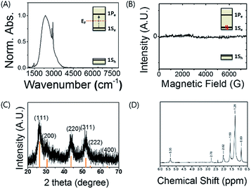
Fig. 1A shows the steady-state intraband (1Se–1Pe) absorption spectrum of HgS CQD in tetrachloroethylene. The half width at half maximum (HWHM) of the HgS CQD is ca. 290 cm−1. The narrow vibrational absorption peaks correspond to symmetric (2920 cm−1) and asymmetric (2890 cm−1) C–H stretch modes of oleylamine, the ligand of the nanocrystal. The shoulder shown at ca. 3200 cm−1 is attributed to the N–H stretch mode of the surface-bound oleylamine ligands.
 | ||
| Fig. 1 (A) Mid-IR intraband absorption spectrum, (B) EPR spectrum of HgS CQD solution, (C) XRD pattern of HgS CQD film and (D) 1H-NMR spectrum of oleylamine bound to the surface of HgS CQDs. | ||
Electron paramagnetic resonance (EPR) spectrum, providing direct information about the magnetic property for the HgS CQD, was obtained (Fig. 1B). In combination with the optical intraband transition in Fig. 1A, the featureless EPR spectrum corresponding to diamagnetism demonstrates the pairing of two electrons in the 1Se state. The featureless spectrum can be understood by referring to the previously reported result.8 Jeong et al. demonstrated that the 1Se state of the HgSe CQD showing the intraband transition is filled with two paired electrons. Therefore, the featureless spectrum obtained here also indicates the DOQS in which the paired electrons occupy the 1Se state. NMR spectroscopy proves the existence of oleylamine, the ligand of the HgS CQD, and corroborates the absence of organic by-product. Furthermore, the mercury-rich HgS CQD is identified by the X-ray photoelectron spectroscopy result tabulated in Table 1.
| Element | Hg 4f | S 2p | C 1s | N 1s | O 1s | Cl 2p |
| Atomic% | 6.0 | 3.6 | 74.1 | 8.0 | 5.6 | 2.2 |
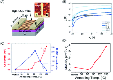
Fig. 2A illustrates the schematic structure of HgS CQD TFT with source/drain metallization and its corresponding optical microscopy (OM) image. A heavily-doped Si wafer with 200 nm thermal SiO2 was used both as a substrate and as a gate electrode for the TFT fabrication.14 The Al electrode was thermally evaporated for the top-contacted transistor geometry using a metal shadow mask, forming a channel length and width of 50 μm and 1000 μm, respectively, as shown at the top right of Fig. 2A. These devices were fabricated shortly after the thermal annealing of HgS CQD film.
It was reported that the thermal treatment of CQD films gives rise to the removal of residual solvent, and therefore further reduces the inter-particle distance.15,16 Thus, the thermal annealing step should be investigated so that the electrical characteristics of the heavily doped HgS CQD film-based devices can be clearly understood and optimized under the configuration of TFT. Fig. 2B shows the series of transfer curves of HgS CQD TFTs annealed at various temperature from 65 to 150 °C and of the pristine. The pristine device (no thermal annealing) exhibited a noticeable current modulation as large as about 10 as a function of gate voltage (VGS) sweep, inferring the effective charge transport after the ligand exchange process. Further increase of the annealing temperature continues to affect the device performance in terms of current on/off ratio (Ion/Ioff) and the on-state current (Ion). For example, HgS CQD TFT annealed at 65 °C showed about 102 Ion/Ioff ratio while Ion was kept almost constant. It appears that a gradual increase of the annealing temperature almost monotonically increases Ion up to 150 °C. However, the Ion/Ioff ratio, as low as about 5, of HgS CQD TFT severely worsened following 150 °C annealing. This negligible current modulation is probably attributed to the quantum confinement loss by the nanocrystal sintering of HgS CQDs.
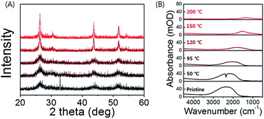
Fig. 2C summarizes the correlation of Ion and the Ion/Ioff ratio as a function of annealing temperature, clearly exhibiting the change of electrical property of HgS CQD films. In our study, 95 °C annealing renders the best Ion/Ioff ratio although 150 °C annealing produces the highest Ion value. It is reasonable that the gradual increase of the Ion/Ioff ratio up to 95 °C results from the efficient packing of individual nanocrystal. In contrast, the attenuation of the Ion/Ioff ratio at above 120 °C is involved with the deterioration of the intraband conduction, based on the XRD spectra change (Fig. 3A). Thus, the annealing at 95 °C seems to be the best condition for thermal treatment for HgS CQD TFTs. This trend also suggests that 95 °C annealing effectively assists the networking of semiconducting CQDs with SCN ligands for efficient charge transport.
 | ||
| Fig. 3 (A) XRD spectra of HgS CQD at corresponding temperature. (B) IR spectra of HgS CQD films after annealing at different temperature. | ||
The field-effect mobility of HgS CQD TFTs as a function of annealing temperature is shown in Fig. 2D. The carrier mobility (μlin) from the linear regime of these devices is used to compare the electrical characteristics of HgS TFTs annealed at the different temperature.
The thermal annealing not only affects the device performance and but also the size of nanocrystal and the intensity of the intraband transition (Fig. 3). X-ray diffraction spectrum exhibits four distinct peaks at (111), (200), (220), and (331), corresponding to the cubic structure of β-HgS CQD in Fig. 3A. Due to the small size of the nanocrystal, the peak width is relatively broad compared to that of bulk HgS. The intensity of the HgS (111) facet indicates that the HgS CQD sample is non-stoichiometrically metal rich, leading to the heavy doping of nanocrystal.8,13 In Fig. 3B, the intraband peak gradually shifts to lower wavenumber under annealing process due to the coupling between wavefunctions of the nearby electrons. It was found that the intensity of the intraband transition peak substantially drops by an order of magnitude with increasing temperature. The significant attenuation of intraband peak intensity is associated with the nanocrystal sintering as well, as shown in the XRD spectra in Fig. 3A, and the field emission scanning electron microscopy (FESEM) in Fig. 4. The spectroscopic investigation of the steady-state intraband transition using FT-IR seems to be qualitatively consistent with the current modulation of TFTs in Fig. 2C. Therefore, it can be inferred that excessive thermal annealing at 150 °C tends to eliminate the quantum confinement characteristics of the intraband transition for the HgS CQDs. Thus, the spectroscopic observation of intraband peaks of HgS CQDs films annealed at the different temperature is correlated with their electrical properties measured and could serve as a reference for predicting the optimized annealing condition.
Similarly, the behaviour of field-effect mobility seems to be significantly influenced by the annealing temperature as well, exhibiting a pseudo-linear increase of μlin. μlin of HgS TFTs annealed at 0, 65, 80, 95, 120, and 150 °C were measured as high as 0.49, 0.15, 0.45, 1.29, 2.20, and 3.80 cm2 V−1 s−1, respectively. Relative high field-effect mobility might be associated with the increased electrons per dots in the doubly occupied quantum states as well as the effective inorganic ligand exchange by a thiocyanate. The increased carrier concentration of disordered semiconductor thin films such as CQDs and amorphous oxides alleviates the carrier trapping by preferentially filling the localized trap states at the lower level of energy states, consequently leading to higher field-effect mobility. In addition, the induced charge carrier concentrations at the interface of the CQD film and SiO2 dielectric layer of HgS TFTs at VGS = 40 V can be estimated by the following eqn (1)17
 | (1) |
To note, the annealing of HgS CQD film at 150 °C substantially degrades the device performance of the transistor which almost lost the on/off switching characteristics. Therefore, the annealing at 95 °C corresponds to the optimized annealing temperature in terms of TFT operation of HgS CQD films. Since the synthesis was carried out at 95–100 °C, it is reasonable to expect the thermal annealing above the temperature to possibly trigger the nanocrystal to sinter. Consequently, the transport characteristics of HgS CQD TFT annealed at 150 °C, which is the highest annealing temperature performed in this study, produces the minimal current modulation during the VGS sweeping. The gradual change of the electrical property is probably related to the onset of quantum dot clustering within HgS semiconducting nanocrystal films.
The high mobility of HgS CQD solid may arise from the intrinsic property of the nonstoichiometric metal-rich HgS CQD with large HgS (111) facet where metal ions are prone to be bonded.8,18,19 The excess metal element of HgS can offer more conducting channels, leading to high mobility based on the eqn (2)
 | (2) |
 | (3) |
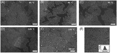
To delve into the change of morphology of the HgS CQDs after thermal annealing, field emission scanning electron microscopy (FESEM) was employed as shown in Fig. 4A–E. Note that the cracks were also observed due to the thermal annealing process. It could cause the performance variation based on these films. So, we carried out the multiple coating of HgS CQDs for alleviated performance deviation. The HgS CQD films, fabricated with HgS CQDs (Fig. 4F), annealed below 120 °C seemed to have the almost negligible difference in morphology. At 150 °C, however, it was found that noticeable agglomeration of HgS CQDs already began. These tens of nm-sized agglomerated HgS nanocrystals should be attributed to the sintering of nanocrystals by the excessive thermal budget. Considering the relation between the morphological variance and the change of the electrical property of HgS CQD films, the lowest current modulation of the devices was probably caused by these aggregates induced by the sintering effect. These fused CQDs would behave as the semi-metallic islands, and consequently attenuate the Ion/Ioff ratio of QD-TFT. Although this sintering effect might appear beneficial to the increase of the on-current of the HgS CQD device, concurrent degradation of current on/off ratio makes it undesirable to be implemented for various application such as sensors. As discussed, the thermal annealing of QD films after the ligand exchange is proved to enhance the device performance by further reducing the gap between CQDs, while excessive thermal budget rather leads to the deterioration.
Conclusions
In conclusion, the electron mobility of the air-stable n-type HgS CQD TFT was first examined at various annealing temperatures. The mobility measured is as high as 1.29 cm2 V−1 s−1 with ca. 102 current on/off ratio after annealing at the optimal temperature of 95 °C. This relatively high field-effect mobility might arise from the increased electrons per dots in doubly occupied quantum state (DOQS) of HgS CQD film as well as the effective ligand exchange and optimal thermal annealing. Annealing the CQD film enhances the carrier transport due to the efficient packing the nanocrystal film and resultant reduced inter-dot distance. It was also observed that excessive thermal budget gives rise to the phase transition from the n-type semiconducting nanocrystal with the intraband quantum confinement to bulk-nanocrystal alloys. These HgS TFTs with effective current control by a gate bias can represent a unique electronic building block with intraband optical properties. Therefore, the air-stable n-doped colloidal HgS CQD TFT with high field-effect mobility under optimized annealing condition will be a promising pathway to the fabrication of low-cost and low-energy-consumed CQD based electronics and optoelectronics.Acknowledgements
This work is supported by the Basic Science Research Program through the National Research Foundation of Korea (NRF) funded by the Ministry of Science, ICT, & Future Planning (NRF-2016R1C1B2013416), the Ministry of Education (NRF20100020209) and the NRF grant funded by the Korea government (MSIP) (No. 2015R1C1A1A01052720).References
- M. V. Kovalenko, L. Manna, A. Cabot, Z. Hens, D. V. Talapin, C. R. Kagan, V. I. Klimov, A. L. Rogach, P. Reiss, D. J. Milliron, P. Guyot-Sionnnest, G. Konstantatos, W. J. Parak, T. Hyeon, B. A. Korgel, C. B. Murray and W. Heiss, ACS Nano, 2015, 9, 1012–1057 CrossRef CAS PubMed.
- P. Guyot-Sionnest, M. Shim, C. Matranga and M. Hines, Phys. Rev. B: Condens. Matter Mater. Phys., 1999, 60, R2181–R2184 CrossRef CAS.
- V. I. Klimov and D. W. McBranch, Phys. Rev. Lett., 1998, 80, 4028–4031 CrossRef CAS.
- D. Yu, C. Wang and P. Guyot-Sionnest, Science, 2003, 300, 1277–1280 CrossRef CAS PubMed.
- K. S. Jeong, Z. Deng, S. Keuleyan, H. Liu and P. Guyot-Sionnest, J. Phys. Chem. Lett., 2014, 5, 1139–1143 CrossRef CAS PubMed.
- Z. Deng, K. S. Jeong and P. Guyot-Sionnest, ACS Nano, 2014, 8, 11707–11714 CrossRef CAS PubMed.
- B. Yoon, J. Jeong and K. S. Jeong, J. Phys. Chem. C, 2016, 120, 22062–22068 CAS.
- J. Jeong, B. Yoon, Y. W. Kwon, D. Choi and K. S. Jeong, Nano Lett., 2017, 17, 1187–1193 CrossRef CAS PubMed.
- M. Liu, O. Voznyy, R. Sabatini, F. P. G. de Arquer, R. Munir, A. H. Balawi, X. Lan, F. Fan, G. Walters, A. R. Kirmani, S. Hoogland, F. Laquai, A. Amassian and E. H. Sargent, Nat. Mater., 2016, 16, 258–263 CrossRef PubMed.
- H. Zhang, J. Jang, W. Liu and D. V. Talapin, ACS Nano, 2014, 8, 7359–7369 CrossRef CAS PubMed.
- S. J. Oh, N. E. Berry, J. H. Choi, E. A. Gaulding, T. Paik, S. H. Hong, C. B. Murray and C. R. Kagan, ACS Nano, 2014, 7, 2413–2421 CrossRef PubMed.
- C. H. Jo, J. H. Kim, J. Kim, J. Kim, M. S. Oh, M. S. Kang, M. G. Kim, Y. H. Kim, B. K. Ju and S. K. Park, J. Mater. Chem. C, 2014, 2, 10305–10311 RSC.
- H. Choi, J. H. Ko, Y. H. Kim and S. Jeong, J. Am. Chem. Soc., 2013, 135, 5278–5281 CrossRef CAS PubMed.
- D. V. Talapin and C. B. Murray, Science, 2005, 310, 86–89 CrossRef CAS PubMed.
- B. A. Ridley, B. Nivi and J. M. Jacobson, Science, 1999, 286, 746–749 CrossRef CAS PubMed.
- M. V. Kovalenko, M. Scheele and D. V. Talapin, Science, 2009, 324, 1417–1420 CrossRef CAS PubMed.
- Y. Liu, J. Tolentino, M. Gibbs, R. Ihly, C. L. Perkins, Y. Liu, N. Crawford, J. C. Hemminger and M. Law, Nano Lett., 2013, 13, 1578–1587 CrossRef CAS PubMed.
- Z. Tang, N. A. Kotov and M. Giersig, Science, 2002, 297, 237–240 CrossRef CAS PubMed.
- W. J. Baumgardner, K. Whitham and T. Hanrath, Nano Lett., 2013, 13, 3225–3231 CrossRef CAS PubMed.
- D. Yu, C. Wang, B. L. Wehrenberg and P. Guyot-Sionnest, Phys. Rev. Lett., 2004, 92, 216802 CrossRef PubMed.
- P. Guyot-Sionnest, J. Phys. Chem. Lett., 2012, 3, 1169–1175 CrossRef CAS PubMed.
Footnote |
| † Electronic supplementary information (ESI) available: Experimental methods and additional figures. See DOI: 10.1039/c7ra07193k |
| This journal is © The Royal Society of Chemistry 2017 |


