
 Open Access Article
 This Open Access Article is licensed under a
 Creative Commons Attribution 3.0 Unported Licence
Vapor-assisted room temperature nanoimprinting-induced molecular alignment in patterned poly(3-hexylthiophene) nanogratings and its stability during thermal annealing†
Kaixuan Wangab,
Xiaohui Lic,
Chao Wangab,
Menxiang Qianab,
Guangzhu Ding *ab and
Jieping Liuab
*ab and
Jieping Liuab
aCollege of Chemistry and Materials Science, Huaibei Normal University, Huaibei 235000, China. E-mail: dinggz@chnu.edu.cn
bAnhui Key Laboratory of Energetic Materials, Collaborative Innovation Center of Advanced Functional Composites of Anhui Province, Anhui 235000, China
cXi'an Jiaotong University Suzhou Academy, Suzhou 215123, China
First published on 16th August 2017
Abstract
Vapor-assisted imprinting technology has been well explored to have good potential for practical application to fabricate topographical nanostructures of polymer film. Herein, we demonstrated that the poly(3-hexylthiophene) (P3HT) nanograting topography can be excellently fabricated via the vapor-assisted room-temperature nanoimprinting lithography (VART-NIL) technique based on a poly(dimethylsiloxane) (PDMS) template and carbon disulfide (CS2) vapor atmosphere. Grazing incidence wide angle X-ray diffraction (GIWAXD) was employed to illustrate that the VART-NIL procedure could not only be used to fabricate the topographical pattern, but also to induce the molecular alignment transition from an edge-on to a face-on alignment, including both form II and form I crystals. Furthermore, according to GIWAXD and atomic force microscopy (AFM) investigations in situ, the stability of the nanopattern surface morphology and molecular alignment of P3HT nanograting film are dependent on the thermal annealing treatment differently. The patterned P3HT nanograting morphology largely disappears into a planar surface at elevated temperatures and the crystallographic structure of the P3HT crystal transfers from form II to form I during the elevated temperature process; however, the nanoimprint-induced face-on molecule alignment of form I conformation surprisingly remains eternal within the distorted nanograting film after the cooling step. Furthermore, the face-on molecular alignment of the form I conformation remained developed and steadily and successively enhanced during the cooling step.
Introduction
Nanoimprinting lithography (NIL) is being investigated as one of the promising methods to fabricate nanostructures for its advantage of high resolution, low cost, and high throughput.1–4 Compared to that of the typical optical lithography, the resolution of the NIL technique is independent of some light factors, such as wave diffraction, scattering, and interference. The NIL method is mainly able to copy the pattern structure defined on a template into a polymer thin film; therefore, it has been significantly developed in the field of polymer nanometre science and technology, especially for semiconducting polymers.5–12 Typically, for the conventional NIL process, the imprinted resist materials are heated to a higher temperature above their glass transition temperature or melting point, and the material is then forced into the cavity of an embossing hard mould (for example, silicon) under the continual application of high pressure. However, there are some limitations associated with the NIL process that have to be carefully solved in detail. First, as the NIL method is investigated as a typical template duplication technique, it is significant to pursue a mould fabrication that is cost-effective, with simple processing and giving good texture stability. Some traditional moulds, such as silicon moulds or anodic aluminium oxide moulds, have been explored for use during the NIL process; however, they are usually time-consuming, involve a complicated process, are simply fragile and crush or are easy to be deformed, and therefore do not meet the requirements for potential application with the NIL technique. Second, the higher pressure applied in the typical nanoimprinting process is inclined to cause the template to crush, the anti-adhesive layer of the template to disappear gradually and the stress within the polymer pattern to sustain for a long time. Third, some conjugated polymers are easily oxidized and decomposed at enhanced temperatures,13,14 and this phenomenon is detrimental to the performance of organic optoelectronic devices applied with use of the corresponding conjugated polymer. Therefore, room temperature nanoimprinting instead of elevated temperature nanoimprinting has been significantly pursued to fabricate the desired nanostructures in conjugated polymer thin films to cut down the shortage of thermal NIL for conjugated polymers.15–18To address these issues, vapour-assisted imprinting technology has been demonstrated to have good a potential for practical application to fabricate patterned structures.19–24 Vapour-assist imprinting technology differs from the traditional NIL method in that this process employs a solvent vapour instead of elevated temperature to soften the resist polymer film. The solvent vapour is able to effectively lower the glass transition temperature and the polymer viscosity by exposing the polymer to vapour, contributing to inducing polymer mobility into the nanocavity of the imprinting mould. Therefore, low pressure imprinting and a lower imprinting temperature protocol can be developed to offer sufficient polymer flow for the patterning process.
Another demonstrated alternative to conventional NIL technology was to use soft lithography techniques based on polydimethylsiloxane (PDMS) mould.23,25–29 PDMS employed as an NIL template is an elastomer and is able to have complete conformal contact with a substrate bearing an even or curved substrate surface. Paul et al. employed a PDMS stamp as an elastomeric mask to fabricate a patterned nanostructure on a curved surface, where the feature size of the pattern could be improved to 175 nm.27 With this techniques, when exposed to a solvent vapour, the PDMS template becomes directly swollen by the solvent and the PDMS mould thus becomes a solvent container during the soft imprinting process.28 The solvent within the PDMS mould diffuses into the polymer resist and contributes to the enhancement of the polymer molecule mobility, which is beneficial for the patterning of the polymer film. Therefore, vapour-assisted NIL technology based on the patterned PDMS as an imprinting mould has significant potential for the large-area pattern fabrication of polymer films.
Furthermore, when imprinting conditions were chosen appropriately during the NIL process, it was demonstrated interestingly that the NIL technique was not only able to fabricate the nanostructures but also to induce the transition of the molecular and crystallographic ordering of imprinted materials which were able to self-organize.9–12,30–32 This indicated that some factors, such as self-organization, nanoconfinement, pressure and rheological chain alignment, had a profound effect on the molecular orientation transition of imprinted materials within the patterned nanostructures. In our previous study, we developed a simple and cost-effective solvent-assisted room-temperature NIL (SART-NIL) method based on the NIL technique.33–36 SART-NIL technical was employed not only to fabricate the poly(3-hexylthiophene) (P3HT) nanostructures but also to prepare the desired morphology in the active layer of ordered bulk heterojunction photovoltaic cells based on uniform P3HT nanostructures surrounded by PCBM material. We also found that the SART-NIL method was not only able to pattern the P3HT polymer film easily, but also could induce a face-on molecular alignment of polymer P3HT for the nanopattern.33,36 As reported, it was revealed that selected solvent vapour treatment behaviour plays a key role in determining their enhanced crystallization or the preferential molecular alignment of a semiconducting conjugated polymer.37–40 Therefore, during the vapour-assisted imprinting process, the role of the vapour in achieving molecular orientation of the polymer cannot be ignored, besides in the pattern formation of the resist layer. Han et al. revealed that a P3HT film with a hierarchical ordered structure was fabricated by a vapour-assisted imprinting in a carbon disulfide (CS2) vapour and the P3HT domains were constituted by uniaxially aligned nanofibrils with chains adopting a flat-on conformation.29 However, a comprehensive understanding of the NIL process in determining the molecular alignment of the semiconducting polymer is unknown and thus forming a precise picture of how vapour-assisted imprinting induces the molecular orientation remains a challenging task, especially for the vapour-assisted room-temperature nanoimprinting process.
In this work, we employ the vapour-assisted room-temperature NIL (VART-NIL) technique based on a PDMS template as a method to fabricate nanogratings on the surface of a P3HT film. The molecular alignment was carefully measured with grazing incidence wide angle X-ray diffraction (GIWAXD) coupled with area detectors. The results indicated that the VART-NIL method induced the π–π stacking of P3HT chains to orientate in a preferential face-on chain alignment. In addition, the thermal stability of the preferential molecule alignment was also investigated for the P3HT nanograting film by the employment of an in situ measurement of thermal annealing. A detailed transition relationship between the molecular alignment and surface pattern morphology during the annealing is also discussed herein.
Experimental
The conjugated polymer P3HT (Mw 50![[thin space (1/6-em)]](https://www.rsc.org/images/entities/char_2009.gif) 000 g mol−1; regioregularity 98%) was purchased from Rieke Metals Inc. and was employed as received.
000 g mol−1; regioregularity 98%) was purchased from Rieke Metals Inc. and was employed as received.
The polymer P3HT was dissolved in chlorobenzene at room temperature to a concentration of 20 mg ml−1 and was then filtered with 0.25 μm polytetrafluoroethylene filters. Silicon sheet was chosen as the substrate (2 cm × 2 cm) and was washed with deionized water, ethanol, acetone and isopropyl alcohol according to the established control procedure. After the silicon sheet was dried, P3HT solution was applied with a spin-casting process onto the silicon sheet surface. The spin-coating process was performed at a constant spin speed (1600 rpm) for 60 s. Then, the polymer films were transferred to a vacuum pumping system for at least 24 h to remove residual solvent.
The patterned P3HT nanograting film was fabricated by employment of the VART-NIL method. The dried polymer film on the substrate surface was loaded into the closed chamber. A patterned PDMS film was chosen as the nanoimprinting mould in advance. The P3HT film was covered with the patterned PDMS mould in a face-to-face alignment. CS2 (1 ml) was injected into the bottom of the closed chamber for the vapour to assist in the nanoimprinting process. Then, the nanoimprinting process was performed under pressure (0.4 bar) at room temperature (23 °C) and held for 72 h. Before releasing the pressure, the closed chamber was opened for 24 h at room temperature and CS2 vapour was allowed to evaporate out from the chamber to solidify the P3HT nanograting. After the PDMS mould was separated off, the patterned P3HT nanograting film was obtained successfully. For the contrast analysis, unpatterned P3HT film was also fabricated by the same process conditions, only with an unpatterned PDMS film. In order to remove the residual solvent, we kept the patterned P3HT polymer film in the vacuum system for about 24 h. The whole fabrication process was carried out at room temperature.
The surface morphology of the samples was characterized using scanning electron microscopy (SEM) and atomic force microscopy (AFM). The SEM images were obtained using Hitachi S-4800 equipment operated at 15 kV voltage. AFM (Multimode 8, Bruker) was employed to indicate the surface morphology of the P3HT samples during the room temperature and thermal annealing process. The temperature zone of thermal annealing was performed from 23 °C to 210 °C in air. The image was recorded using the tapping mode. The X-ray diffraction data were obtained at beamline BL14B1 of the Shanghai Synchrotron Radiation Facility (SSRF) using X-rays with a wavelength of 1.2398 Å. The detailed information about beamline BL14B1 can be found in a previous report.41 GIWAXD measurements were performed at the BL14B1 beamline and the incident angle of the X-ray beam was 0.18°. Data conversion to q space was obtained by calibration using LaB6 powder. The mediate beam stop was put down to block the primary beamline for two-dimensional (2D) scanning. During the GIWAXD measurements of the thermal annealing, the samples were treated in situ with the aid of fixed heating equipment. The thermal annealing process was carried out by the same procedure as used for the controlled temperature AFM measurements.
Results and discussion
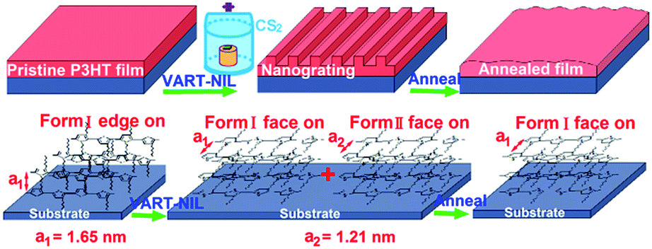
We demonstrate here the VART-NIL technique based on a PDMS template as a method to fabricate nanogratings on the surface of P3HT film. The schematic preparation process of the P3HT nanograting film is illustrated in Scheme 1. The VART-NIL process based on a PDMS template consists of three main preparation steps. First, pristine P3HT film is obtained by spin-coating its solution onto the silicon sheet surface. Second, the dried polymer film on the substrate surface is loaded into a closed chamber and the NIL process is completed under a vapour atmosphere of CS2 at room temperature, where the PDMS template is allowed to adhere slowly onto the polymer surface face to face. Third, after the PDMS mould is separated off, the patterned P3HT nanograting film is successfully obtained.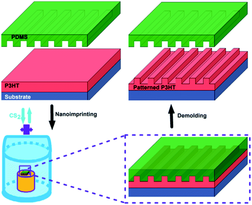 | ||
| Scheme 1 Schematic of the fabrication process of the P3HT nanograting film assisted by the VART-NIL method. | ||
The thickness of the pristine P3HT film can be mainly controlled by its solution concentration and spin-coating speed. In order to eliminate the effect of the residual solvent within the pristine film on the pattern process of the polymer film, it was necessary to remove completely the residual solvent using a vacuum pumping system. The whole nanoimprinting process was performed for sufficient time under CS2 vapour and at room temperature. A patterned PDMS film was employed as the NIL mould, where the elastomeric PDMS mould could have complete conformal contact with the polymer surface.25–29 In addition, the PDMS mould surface cannot be treated to further modify it and it is very easy to separate from the polymer surface after nanoimprinting due to there only being a weak interaction between the polymer and PDMS. Solvent CS2 vapour could be absorbed into the PDMS mould internally and thus the vapour molecules diffuse into the polymer thin film as a result of the solvent concentration gradient between the polymer and mould surface. Polymer molecules also swell or deform slightly, which contributes to fully filling the whole nanocavity of the patterned PDMS mould during the VART-NIL process. Thus, the fabrication process of the polymer pattern is developed under vapour assistance and at room temperature, and hence this is noted as the VART-NIL method. In addition, enough nanoimprinting time is needed to ensure the successful regularity and integrity of the polymer pattern due to the slow processing in the polymer swelling. Before releasing the pressure, the closed chamber was opened to allow CS2 vapour to evaporate out from the chamber to stabilize the P3HT nanograting pattern. The patterned PDMS mould is not damaged during the NIL procedure and is able to be used again to fabricate the nanograting film completely. Therefore, this indicates that the whole preparation of P3HT nanogratings based on the VART-NIL method is simple and cost effective.
Fig. 1 shows the top-down SEM images of the PDMS mould surface and the patterned P3HT nanograting surface. It can be seen that the patterned PDMS mould, shown in Fig. 1a, consists of arrays of lines bearing a trench ∼275 nm wide and a ∼550 nm distance between the adjacent nanograting (period). After the VART-NIL protocol, the patterned P3HT nanograting film of ∼275 nm line width with a period of ∼550 nm was obtained, as shown in Fig. 1b. Both the line width and the period of the replication match the structural dimensions of the patterned PDMS mould. The successful nature of the replication protocol is also shown in the AFM height image in Fig. 2 for the PDMS mould and the patterned P3HT nanograting film, which come from the same samples investigated in Fig. 1. A detailed investigation of the topographical structure was performed through the corresponding cross-sectional curves, as given in the ESI in Fig. S1.† The PDMS mould and P3HT nanograting film both displayed regular and periodic topographical morphology and the same structure dimension, identical to the results in the SEM images shown in Fig. 1. The patterned P3HT nanograting film was fabricated uniformly, with a pattern height of about 75 nm, a perfect replica of PDMS mould. In addition, no collapses or distortion of the P3HT nanograting topography were observed obviously. Thus, this illustrates that the polymer molecule is able to flow into and fill the nano-cavities of the patterned PDMS mould conveniently in a vapour-swollen plasticized state at room temperature. Therefore, this illustrated that the VART-NIL method based on the PDMS template can be employed to fabricate patterned nanograting topography on the surface of P3HT thin film, and further that this technique possess high replication fidelity for the polymer pattern.
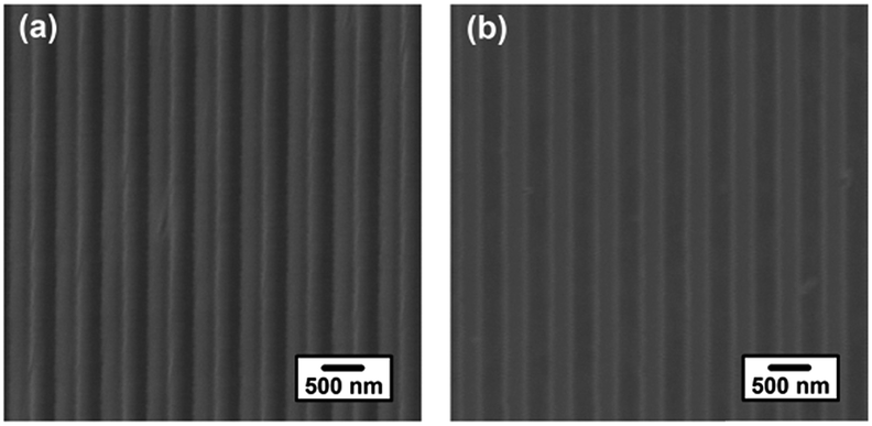 | ||
| Fig. 1 Top-down SEM images of the PDMS mould surface (a) and patterned P3HT nanograting surface (b). | ||
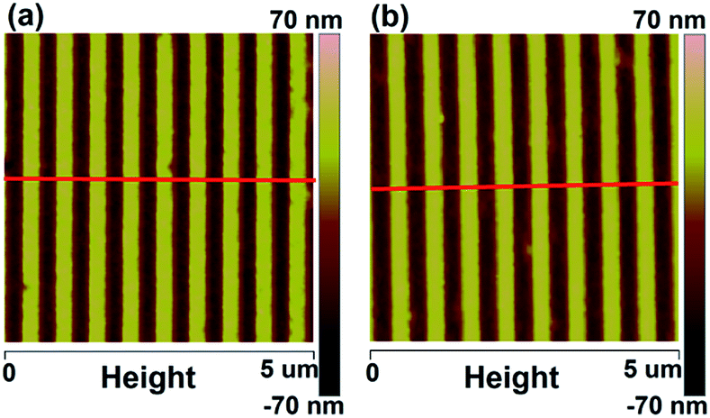 | ||
| Fig. 2 AFM height images of the PDMS mould (a) and patterned P3HT nanograting film (b). The red lines within the images indicate the directions of the cross-sectional curves (Fig. S1 of ESI†). | ||
It was reported that the NIL technique was not only able to fabricate the nanostructures but also to induce transition of the molecular and crystallographic ordering of imprinted materials which were able to self-organize.30–36 In order to probe the effect of the VART-NIL procedure on the molecular alignment of P3HT polymer molecule, GIWAXD measurements of the polymer P3HT film before and after patterning were performed, with the corresponding results shown in Fig. 3 and 4. The X-ray diffraction data were obtained at the Synchrotron Radiation Facility using an X-ray with a wavelength of 1.2398 Å, and a schematic illustration of the X-ray measurement is shown in Fig. S2 in the ESI.† The measured sample was loaded on the surface of the sample stage of the device equipped with a heating device and with accurate control of the incident angle of the X-ray. A 2D charge-coupled device detector was used to investigate the diffraction information. In addition, we note here that, in order to better investigate the molecular alignment exactly, the GIWAXD measurement of P3HT nanograting film was examined in the line direction of the nanograting parallel and perpendicular to the direction of the incident X-rays, respectively. “Parallel” and “Vertical” refer to the line direction of the P3HT nanograting parallel and normal to the direction of the incident X-rays.
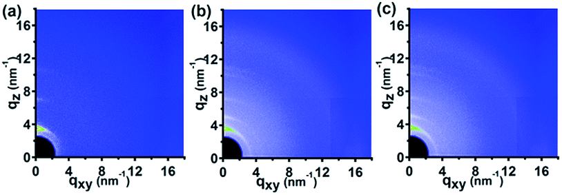 | ||
| Fig. 3 The two-dimensional (2D) GIWAXD images of the P3HT thin film for: (a) the pristine film; (b) P3HT nanograting film with the nanograting direction parallel to the direction of incident X-rays; (c) P3HT nanograting film with the nanograting direction vertical to the direction of incident X-rays. | ||
 | ||
| Fig. 4 The one dimensional (1D) GIWAXD intensity curves of pristine and nanograting films integrated along the qz direction (a) and the qxy direction (b). The integrated data are collected from the 2D images as shown in Fig. 3. Here, we define “Parallel” and “Vertical” as the line directions of P3HT nanograting parallel and vertical to the direction of incident X-rays. | ||
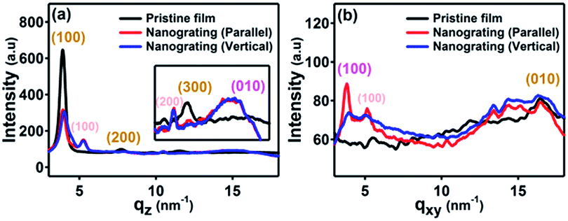
Here, we also adopted the standard crystallographic notation for the P3HT polymer, where the (h00) plane, (010) plane and (001) plane are referred to as the layering direction, π–π direction and backbone direction, respectively.30–36 Fig. S3 in the ESI† shows two typical edge-on and face-on molecule alignments of P3HT molecule chains on the substrate surface, and the lattice parameters a, b and c are distances between the backbones, π–π stacking distance and distance between the side chains, respectively. The diffraction vectors qxy and qz refer to the diffraction information parallel and vertical to the substrate surface, while the diffraction peaks at q = 3.8 nm−1 and q = 16.8 nm−1 correspond to the (100) plane and (010) plane reflection signals of the P3HT crystal,32–36 respectively.
Fig. 3 indicates the 2D GIWAXD images of the pristine polymer film and nanograting film with the grating direction parallel or vertical to the direction of incident X-rays. In order to better acquire diffraction information, one dimensional (1D) intensity curves of GIWAXD images were also integrated both along the qz and qxy directions, as shown in Fig. 4. These indicated that a single edge-on molecular alignment was present for the pristine P3HT film, which could further be revealed by only the (h00) and (010) reflections appearing in the qz and qxy directions respectively, which is consistent with the previous reports.32–36 However, this is complicated for the diffraction patterning of the patterned P3HT nanograting film. First, apart from the obvious (h00) and (010) reflection peaks along the qz and qxy directions respectively, additional reflections of the (010) plane along the qz direction and (100) plane along qxy direction are present for the diffraction patterning of the P3HT nanograting films simultaneously. These additional reflections of the (010) and (100) peaks confirm that a face-on molecular orientation is induced for the P3HT nanograting film during the VART-NIL process. The presence of preferential face-on molecule alignment within the P3HT nanograting film may be due to the confinement growth of P3HT crystals within the nanocavity space of the PDMS mould.33,34 In addition, it can be inferred that there is still an edge-on chain alignment for the patterned nanograting film, which is revealed by the reflection patterns of the (h00) plane and (010) plane along the qz and qxy directions, respectively. This firm molecular alignment may result primarily from the contribution of a residual layer beneath the nanograting pattern.34 Second, the GIWAXD profile of the nanograting film shows the presence of the reflection peak from the (100) mille plane of the crystallographic structure, which is indicated at q = 5.2 nm−1. The obviously increased q value of the P3HT crystal must result from the crystallographic transition from form I to form II, which is similar to the transition of the conjugated polymer as reported previously.29,39,40,42 The crystallographic transition from the typical form I to form II of polythiophene was generally obtained by exposing the polymer to solvent CS2 vapour atmosphere treatment. Compared to the form I, the increase in the diffraction q value indicates that the distance between the alkyl chains is slightly reduced for the form II. Third, as for the diffraction pattern of the P3HT form II crystal, (h00) reflection peaks can be investigated evidently both in the qz and qxy directions; however, no illustration of a (010) plane reflection of form II (different from the form I) was indicated along the qz and qxy directions, or in other words the π–π stacking distance, which is associated with the (010) plane reflection, was unchanged significantly for the form I and form II crystal conformations investigated in this paper. Thus, for the nanoimprinted P3HT nanograting film, it indicated that the (100), (200) and (010) peaks of form II crystal conformation emerge along the qz direction, while the (100) and (010) peaks of form II crystal conformation also come up along the qxy direction. Together, there are both edge-on and face-on molecular alignments of the form II crystal for the P3HT nanograting film. Here, the face-on molecular alignment of form II crystal arises mainly from the P3HT nanograting structure, which occurs by the same induced growth effect as the face-on molecular alignment of form I, and we also believe that the edge-on molecule alignment of form II crystal may mainly result from the effect of a residual layer beneath the nanograting pattern. Fourth, in order to illustrate the crystallographic structure in detail, investigation of the GIWAXD signal of the nanograting film was performed according to the line direction of the nanograting parallel or perpendicular to the direction of incident X-rays. The GIWAXD signals did not vary for the P3HT nanograting films parallel or perpendicular to the direction of incident X-rays, showing that the alignment of chains within the nanograting film was identical for the orthogonal nanograting line direction. In addition, the invariance of all the reflection peak positions was noted for the P3HT polymer before and after the VART-NIL process, except for the magical emergence of the form II crystal conformation. Thus, this provides evidence that there is an absence of crystallographic dimensional change for the form I P3HT crystal before and after the VART-NIL procedure. The schematic illustration of the molecular alignment transition of the P3HT nanograting film during the fabrication step assisted by VART-NIL is shown in Scheme 2.
 | ||
| Scheme 2 Schematic of the molecular alignment transition of P3HT nanograting film during the fabrication step assisted by VART-NIL and the thermal annealing process. | ||
Here, it is noted that the significant face-on molecular alignment of form I and form II crystals cannot be induced without the pattern processing as revealed by the GIWAXD pattern of the vapour annealing P3HT film, as shown in Fig. S4 of the ESI.† Vapour annealing of the P3HT film can be achieved under the same conditions as the fabrication of nanograting film with an unpatterned PDMS film rather than patterned PDMS film as the mould. This indicates that there are only (h00) and (010) reflection patterns of form I and form II crystal appearing in the qz and qxy directions, respectively. Thus, it can be concluded that the P3HT molecular chains of form I and form II crystals only adopt an edge-on molecule alignment to the substrate after the single vapour treatment with CS2 atmosphere rather than the VART-NIL process. This confirms again that, as discussed above, the induced face-on alignment of form I and form II crystals is contributed mainly by the pattern process during the VART-NIL procedure and this preferential face-on alignment of form I and form II crystals exists in the pattern structure of the P3HT nanograting film rather than in the residual layer beneath the nanograting pattern.
This indicates that, as discussed above, the face-on alignment of form I and form II crystal can be induced during the fabrication process of nanograting P3HT film assisted by the VART-NIL procedure. In our previous study, we demonstrated that the NIL method was not only able to facilely fabricate the P3HT nanopillars, but also to induce the face-on molecular orientation of P3HT existing in the nanopillars.33,34 The preferential face-on orientation within P3HT nanopillars mainly results from the confinement of rod-like crystals with their π–π stacking direction along the rod axis. Therefore, understanding of the nanopatterned contact or confinement is important for the formation of a face-on arrangement. However, the NIL process is a complicated process and depends on many factors, such as temperature, pressure, nano-space and interface interaction. Thus, a comprehensive understanding of the NIL process in determining the molecular orientation has not been achieved yet and forming a precise picture of how nanoimprinting induces the molecular orientation remains a challenging task. More comments about the mechanism in this paper can be described very limitedly. However, we can ensure that the significant face-on molecular alignment of form I and form II crystals cannot be induced without pattern processing, as revealed by the GIWAXD pattern of vapour annealing P3HT film. In all, we indicate here that the induced face-on alignment of form I and form II crystals is dependent mainly on the patterning process during the VART-NIL procedure, while a deeper understanding of the mechanism of the induced alignment during the NIL method will be explored in the next report as part of our continual research.
Therefore, as illustrated by the results and discussion above, the VART-NIL procedure is able not only to fabricate the topographical nanostructures of a nanograting P3HT film, but is also able to induce the molecular alignment transition from an edge-on to face-on alignment, including both the face-on conformations of form I and form II crystals.
As reported, the crystallographic conformation of the P3HT crystal was able to transform from form I to form II surprisingly after the thermal annealing treatment.29,40 In fact, thermal stability of the surface morphology and internal molecule alignment plays a significant role in determining the semiconducting polymer applications. Therefore, in order to investigate the thermal stability of the surface morphology and internal molecular alignment of form I and form II conformations of the patterned P3HT nanograting film, a thermal annealing treatment on the nanopatterned P3HT film was performed. Fig. 5 shows the 2D GIWAXD image and AFM height profile of the P3HT nanograting film after thermal annealing. The thermal annealing procedure was performed under a fixed temperature (210 °C) for 15 min and then the annealed film was cooled down to room temperature for the AFM and GIWAXD measurements. 1D GIWAXD intensity curves of the P3HT nanograting film (before and after thermal annealing) integrated along the qz and qxy directions were also plotted and can be found in the ESI (Fig. S5†). These indicate that, for the annealed nanograting film, both the (h00) and (010) diffraction planes of form I conformation of the P3HT crystal are only present in the qz and qxy directions simultaneously and there is no other additional diffraction peaks existing in the annealed pattern film. Thus, it can be inferred that there are two key results. First, the P3HT crystal is crystallized in the form I conformation after the thermal annealing treatment and the P3HT molecules do not adopt any form II conformation to arrange crystallization. This further confirms that the crystallographic transition of the P3HT crystal from form II to form I emerges after the thermal annealing treatment and that the stability of the form II conformation is dependent on the thermal process significantly. Second, it can be inferred that a mixture of edge-on and face-on chain alignments of the form I crystal exists in the nanograting P3HT film after thermal annealing. Except for an edge-on chain orientation that arises primarily from the residual layer beneath, the nanoimprinting-induced face-on molecular alignment of form I by the VART-NIL process is retained in the annealed P3HT nanogratings, independently of the effect of the thermal annealing treatment. In addition, a pronounced difference can be seen for the diffraction intensity of the retained reflection peaks before and after thermal annealing. This enhancement in the intensity may result from the improved crystallization or reorientation during the thermal annealing processing. It was also noted that there was a weak fluctuation of the crystallographic dimensions in the form I conformation, as revealed by the negligible change in the reflection peak position before and after the annealing.
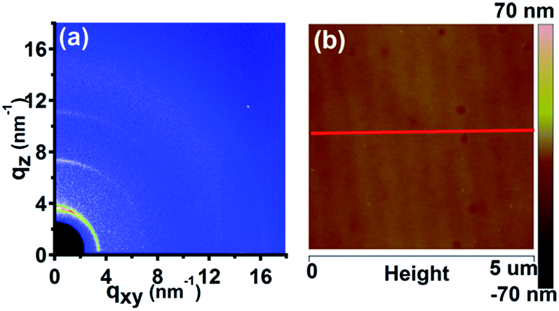 | ||
| Fig. 5 2D GIWAXD image (a) and AFM height image (b) of P3HT nanograting film after thermal annealing. The thermal annealing is performed under a fixed temperature (210 °C) for 15 min and then the thin film is cooled down to room temperature (23 °C). The red line within image (b) indicates the direction of the cross-sectional curve (Fig. S6 of ESI†). | ||
The cross-sectional height curve of the P3HT nanograting film after thermal annealing is presented in Fig. S6 of the ESI.† This indicates that the surface structure of the annealed P3HT nanograting film is not as perfect as the morphology before thermal annealing. It can thus be inferred that the thermal annealing treatment leads to a rapid decay in the nanostructure profile and a smoothing-out surface is formed finally for the annealed nanograting film with the increasing temperature, although an obscure profile of a nanopatterned structure still exists, more or less. Thus, this indicates that the stability of the surface morphology of the nanograting pattern profile significantly depends on the thermal annealing processing.
Therefore, it explains why the patterned P3HT nanograting morphology largely disappears at elevated temperature and the crystallographic structure of the P3HT crystal transfers from form II to form I after the thermal annealing treatment; however, the nanoimprint-induced face-on molecular alignment of form I conformation surprisingly remains within the annealed nanograting film. The thermal annealing treatment has a different effect on the stability of the nanopatterned surface and molecular alignment of the P3HT nanograting film. In order to illustrate the effect of thermal annealing on the transition process for the morphology and alignment in detail, GIWAXD and AFM measurements in situ were performed to investigate the development processing.
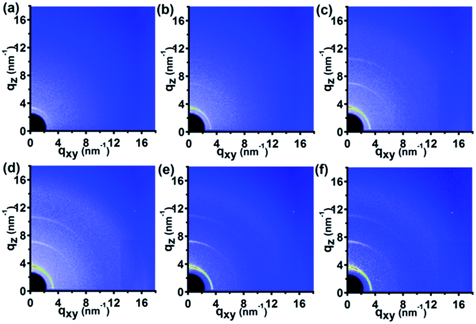
Fig. 6 shows the 2D GIWAXD patterns of the P3HT nanograting film during the in situ elevated temperature for various temperatures from 23 °C to 210 °C. To better investigate the transition process of the molecular alignment, 1D integrated intensity curves of GIWAXD images along the qz and qxy directions were plotted and are displayed in Fig. S7 of the ESI.† First, except for the diffraction peaks discussed above, no additional or new diffraction peak was found during the heating process, indicating no new crystallography structure arises from the elevated temperature process. Second, as for the edge-on and face-on molecular alignments of form II, the diffraction pattern of the P3HT crystal showed a concomitant and substantial transition alongside the increased temperature, and the diffraction peaks of form II in the qz or qxy directions quickly diminished until they vanished completely when the heating temperature was increased to 120 °C. Third, as for the P3HT crystal of form I, the diffraction peaks of the (h00) plane in the qz direction and (010) plane in the qxy direction, which are associated with the edge-on molecule alignment, and the diffraction peaks of the (h00) plane in the qxy direction and (010) plane in the qz direction associated with the face-on molecule orientation developed in a complicated manner. The intensity of all he diffraction peaks was first enhanced significantly and successively as the temperature was increased from 23 °C to 120 °C but then the intensity decreased successively when the temperature increased more from 120 °C to 210 °C. All the peak intensities were not present or were negligible at heating temperature of 210 °C, indicating that melting of P3HT polymer crystal had occurred, resulting from the heating energy. However, it was interesting to see that, during the heating temperature from 23 °C to 120 °C, the diffraction peak intensity of the form II crystal decreased successively but the peak intensity of the form I crystal was enhanced step by step. It can be inferred from this that the crystallographic transition of form II to form developed indeed during the elevated temperature process.
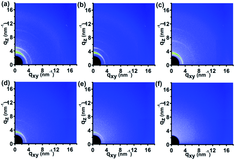 | ||
| Fig. 6 The 2D GIWAXD patterns of P3HT nanograting film during the elevated temperature process in situ for various temperatures: (a) 23 °C, (b) 90 °C, (c) 120 °C, (d) 150 °C, (e) 180 °C, and (f) 210 °C. | ||
Fig. 7 shows the 2D GIWAXD patterns of the P3HT nanograting film during the in situ cooling temperature procedure for various temperatures from 180 °C to 23 °C, while the 1D integrated intensity curves along the qz and qxy directions are also indicated in Fig. S8 of the ESI.† It was found that there was only the presence of diffraction peaks of the P3HT crystal in the form I conformation, associated with the diffraction peaks of the (h00) and (010) planes in both the qz and qxy directions, and no other diffraction peak was added during the whole cooling step. That is to say, the crystallographic structure of form II did not reappear again for the P3HT chains during the decreased temperature process. It can be strongly inferred from this that the mixture of edge-on and face-on chain alignments in the form I conformation re-exists in the annealed P3HT nanograting film, same as in the thermal annealing before. Furthermore, the peak intensity of the all peaks emerged and was enhanced concomitantly and successively during the cooling step due to the presence of polymer crystallization once again. As discussed above, the edge-on chain orientation arises primarily from the residual layer. Therefore, this strongly confirms that the nanoimprint-induced face-on molecule alignment of nanograting film in the form I conformation is retained, somewhat surprisingly, after the whole annealing processing. We believe this preservation of the face-on molecular alignment might result from the enhanced crystallization or reorientation of P3HT molecular chains during the annealing process.
 | ||
| Fig. 7 The 2D GIWAXD patterns of P3HT nanograting film during the cooling temperature process in situ for various temperatures: (a) 180 °C, (b) 150 °C, (c) 120 °C, (d) 90 °C, (e) 60 °C, and (f) 23 °C. | ||
It is noted that, according to a further investigation on the integrated GIWAXD curves as shown in Fig. S7 and S8 of the ESI,† a slight variance of peak position in the nanograting film can be observed during both the elevated and cooling temperature processes. This indicates that for the (h00) reflection (including the P3HT crystal, both in form II and form I), the peak position is reduced slightly along the q value during the elevated temperature step and then the position is increased feebly during the cooling process. However, as for the (010) reflection (including the P3HT crystal both in form II and form I), the position first increases alongside the heating step but then recovers to a limited degree during the decreased temperature process. But it is limited for the variation of the peak position of both the (h00) and (010) reflections. Thus, the slight change in the diffraction peak position refers to a feeble or ignored deformation or fluctuation of the crystallographic dimensions for the P3HT polymer crystal both in form II and form I.
Therefore, according to the in situ GIWAXD measurement of the P3HT crystal during the whole annealing process, the crystallographic structure transition of P3HT crystal from form II to form I occurs in the elevated temperature step in the thermal annealing procedure, and the face-on molecular alignment of form I conformation is also enhanced for the P3HT polymer chains during the transition from form II to form I. Furthermore, the face-on molecular alignment of form I conformation remains developed and is enhanced steadily and successively during the cooling step, although it is diminished and finally vanishes completely during the higher heating temperature step (above 120 °C) of the elevated temperature process.
We note here that pure heating annealing treatment cannot induce the molecular alignment transition from edge-on to face-on orientation during the thermal annealing procedure. This can be illustrated by the absence of a molecular alignment change of the vapour-annealed P3HT film under the same annealing conditions. The 1D GIWAXD intensity curve of the vapour-annealed P3HT film after thermal annealing treatment was investigated, as shown in Fig. S9 of the ESI.† The vapour-annealed P3HT film was obtained in the same conditions as the fabrication of nanograting film with an unpatterned PDMS film rather than with a patterned PDMS film (equal to the sample fabrication of Fig. S4†). Then, the vapour-annealed P3HT film was heated from 23 °C to 210 °C and next cooled from 210 °C to 23 °C to complete the thermal annealing treatment procedure. It was indicated that there was a single edge-on chain alignment of form I conformation arising within the vapour-annealed film after the thermal annealing, inferred from only the (h00) and (010) reflections appearing in the qz and qxy directions, respectively. As discussed in the Fig. S4,† the molecular alignment of the vapour-annealed P3HT film only behaved as an edge-on orientation (both form II and form I) before the thermal annealing. Thus, for the thermal stability, the molecular orientation of the vapour-annealed P3HT film is preferential and there is an absence of other chain alignments during the annealing process. Therefore, pure thermal inducement can be ruled out to determine the presence or retaining of the face-on molecular orientation in the form I conformation and there is no direct connection between the presence of the face-on molecular alignment in form I after the thermal annealing treatment and the edge-on molecular orientation in form II and form I before the thermal annealing.
This indicates that the crystallographic transition of form II to form I indeed develops during the elevated temperature process and all the peak intensities are not present or negligible at a heating temperature of 210 °C. However, the crystallographic structure of form II cannot reappear again for P3HT chains during the decreased temperature process, which confirms that the nanoimprint-induced face-on molecular alignment of the nanograting film in the form I conformation is retained, somewhat surprisingly, after cooling to room temperature. Up to now, the mechanism of the transition and retaining was still considered complicated and unclear and we were only able to point out that pure heating annealing treatment cannot induce the molecular alignment transition from an edge-on to face-on orientation during the cooling procedure. Therefore, we infer that this preservation of the face-on molecular alignment might result from the enhanced crystallization or reorientation of P3HT molecule chains during the cooling process. The detailed mechanism will be explored in further work.
Fig. 8 shows the AFM height images of the P3HT nanograting film under the in situ thermal annealing treatment, while the cross-sectional height curves are also shown in Fig. S10 of the ESI.† These indicate that the topographic structure of the nanograting profile changes little by little with the temperature increasing from 50 °C to 150 °C during the thermal annealing process. The relatively uniform and regular nanograting profile cannot be found at 150 °C and there is an obvious distortion or deformation towards a planar surface. In addition, it was illustrated that the height of the nanograting changes significantly from ∼70 nm to ∼5 nm alongside the annealed temperature increasing from 50 °C to 150 °C. The deformation of the P3HT topographic structure may be driven by the enhancement of internal tension due to the elevated temperature during the thermal annealing.43 Furthermore, it was indicated that the temperature of the evolution of the surface topography structure into a planar surface or its collapsing was close to 150 °C. However, with an elevated temperature close to 150 °C during the heating procedure, the crystallographic structure transition from form II to form I is developed completely and the mixed alignment of face-on and edge-on alignments in the form I crystal remain present for the nanograting film, as discussed above. Therefore, this firmly confirms again that the stability of the topographic structure on the surface of nanograting film depends on the thermal temperature and that the thermal temperature plays a different role in determining the thermal stability of the topographic morphology and molecular alignment for the P3HT nanograting film.
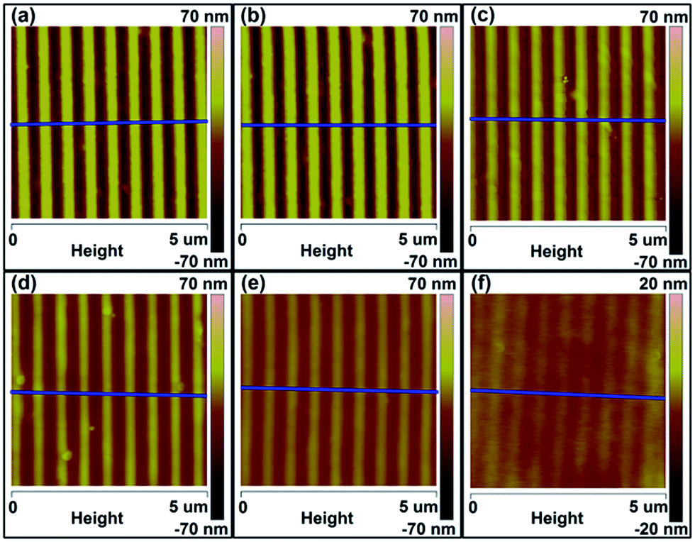 | ||
| Fig. 8 AFM height images of P3HT nanograting film under the thermal annealing treatment in situ for various temperatures: (a) 50 °C, (b) 70 °C, (c) 90 °C, (d) 110 °C, (e) 130 °C, and (f) 150 °C. The blue lines within images show the directions of the cross-sectional curves (Fig. S10 of ESI†). | ||
The schematic illustration of the molecular alignment transition of the P3HT nanograting film during the fabrication step assisted by VART-NIL and the thermal annealing process is shown in Scheme 2. As discussed above, there is only the presence of the edge-on chain alignment for the pristine polymer film as prepared. During the fabrication process of the P3HT nanograting film assisted by the VART-NIL technique, the VART-NIL procedure is able not only to fabricate the topographical nanostructures of the P3HT nanograting film, but also to induce the molecular alignment transition from an edge-on to face-on alignment, including both the face-on conformation of form I and form II crystals. Then, the thermal annealing treatment has a different effect on the stability of nanopattern surface and molecular alignment of P3HT nanograting film. The patterned P3HT nanograting morphology largely disappears at elevated temperature and the crystallographic structure of the P3HT crystal transfers from form II to form I after the thermal annealing treatment; however, the nanoimprint-induced face-on molecule alignment of form I conformation remains, surprisingly, within the annealed nanograting film.
Conclusions
Together, here we employed the VART-NIL technique based on a PDMS template as a method to fabricate a nanograting structure on the surface of a P3HT film. It was illustrated that the VART-NIL method based on a PDMS template could be employed to fabricate a patterned nanograting topography structure successfully and this technique was able to possess a high replication fidelity for the polymer pattern. A single edge-on molecular alignment was present for the pristine P3HT film. However, for the nanoimprinted P3HT nanograting film, there were both edge-on and face-on molecular alignments of form II and form I crystals for the P3HT nanograting film. The edge-on molecule alignment of form II and form I crystals may mainly result from the effect of the residual layer beneath the nanograting pattern. Thus, the VART-NIL procedure was able to induce the molecular alignment transition from an edge-on to face-on alignment, including both the face-on conformation of form I and form II crystals. In order to investigate the thermal stability of the surface morphology and the internal molecular alignment of form I and form II conformations within the patterned P3HT nanograting film, a thermal annealing treatment was performed on the nanopatterned P3HT film. The thermal annealing treatment has a different effect on the stability of the nanopatterned surface and molecular alignment. The crystallographic transition of form II to form I was investigated during the elevated temperature process from 23 °C to 120 °C; however, the nanoimprint-induced face-on molecular alignment of the nanograting film was only retained, in the form I conformation after the cooling temperature process. It was interesting that the relatively uniform and regular nanograting profile could not be found at 150 °C and there was an obvious distortion or deformation towards a planar surface. This investigation will provide new insights and guidance for the fabrication of topographical structures and the molecular alignment of conjugated polymer.Conflicts of interest
There are no conflicts to declare.Acknowledgements
This work is financially supported by the National Natural Science Foundation of China (No. 21504028), Natural Science Foundation of Educational Committee of Anhui Province (KJ2015A119), Innovation Team of Design and Application of Advanced Energetic Materials and the Collaborative Innovation Center of Advanced Functional Composites in Anhui Province. The authors also thank beamline BL14B1 (Shanghai Synchrotron Radiation Facility) for providing the beam time and helps during experiments.Notes and references
- S. Y. Chou, P. R. Krauss and P. J. Renstrom, Appl. Phys. Lett., 1995, 67, 3114 CrossRef CAS.
- C. Yen, F. Wu, H. Cheng, H. Sheu, F. Tang and W. Chou, RSC Adv., 2014, 4, 58342–58348 RSC.
- L. J. Guo, J. Phys. D: Appl. Phys., 2004, 37, R123 CrossRef CAS.
- L. J. Guo, Adv. Mater., 2007, 19, 495–513 CrossRef CAS.
- M. Behl, J. Seekamp, S. Zankovych, C. M. Sotomayor Torres, R. Zentel and J. Ahopelto, Adv. Mater., 2002, 14, 588–591 CrossRef CAS.
- F. Di Benedetto, A. Camposeo, S. Pagliara, E. Mele, L. Persano, R. Stabile, R. Cingolani and D. Pisignano, Nat. Nanotechnol., 2008, 3, 614–619 CrossRef CAS PubMed.
- M. S. Kim, J. S. Kim, J. C. Cho, M. Shtein, L. J. Guo and J. Kim, Appl. Phys. Lett., 2007, 90, 123113–123116 CrossRef.
- E. Mele, F. Di Benedetto, L. Persano, R. Cingolani and D. Pisignano, Nano Lett., 2005, 5, 1915–1919 CrossRef CAS PubMed.
- Z. Hu, B. Muls, L. Gence, D. A. Serban, J. Hofkens, S. Melinte, B. Nysten, S. Demoustier-Champagne and A. M. Jonas, Nano Lett., 2007, 7, 3639–3644 CrossRef CAS PubMed.
- Z. Zheng, K. H. Yim, M. S. M. Saifullah, M. E. Welland, R. H. Friend, J. S. Kim and W. T. S. Huck, Nano Lett., 2007, 7, 987–992 CrossRef CAS PubMed.
- M. Aryal, K. Trivedi and W. Hu, ACS Nano, 2009, 3, 3085–3090 CrossRef CAS PubMed.
- H. Hlaing, X. Lu, T. Hofmann, K. G. Yager, C. T. Black and B. M. Ocko, ACS Nano, 2011, 5, 7532–7538 CrossRef CAS PubMed.
- N. E. Voicu, S. Ludwigs, E. J. W. Crossland, P. Andrew and U. Steiner, Adv. Mater., 2007, 19, 757–761 CrossRef CAS.
- X. He, F. Gao, G. Tu, D. Hasko, S. Huttner, U. Steiner, N. C. Greenham, R. H. Friend and W. T. S. Huck, Nano Lett., 2010, 10, 1302–1307 CrossRef CAS PubMed.
- D. Pisignano, L. Persano, M. F. Raganato, P. Visconti, R. Cingolani, G. Barbarella, L. Favaretto and G. Gigli, Adv. Mater., 2004, 16, 525–529 CrossRef CAS.
- F. Di Benedetto, A. Camposeo, S. Pagliara, E. Mele, L. Persano, R. Stabile, R. Cingolani and D. Pisignano, Nat. Nanotechol., 2008, 3, 614–619 CrossRef CAS PubMed.
- E. Mele, A. Camposeo, M. De Giorgi, F. Di Benedetto, C. De Marco, V. Tasco, R. Cingolani and D. Pisignano, Small, 2008, 4, 1894–1899 CrossRef CAS PubMed.
- S. Pagliara, A. Camposeo, E. Mele, L. Persano, R. Cingolani and D. Pisignano, Nanotechnology, 2010, 21, 215304 CrossRef PubMed.
- E. King, Y. Xia, X.-M. Zhao and G. M. Whitesides, Adv. Mater., 1997, 9, 651–654 CrossRef.
- D. Y. Kang and H. H. Lee, Appl. Phys. Lett., 2000, 76, 870–872 CrossRef.
- N. E. Voicu, S. Ludwigs, E. J. W. Crossland, P. Andrew and U. Sreiner, Adv. Mater., 2007, 19, 757–761 CrossRef CAS.
- R. Mukherjee, G. K. Patil and A. Sharma, Ind. Eng. Chem. Res., 2009, 48, 8812–8818 CrossRef CAS.
- K. L. Lai, M. H. Hon and I. C. Leu, J. Micromech. Microeng., 2011, 21, 075013 CrossRef.
- J. Liu, Q. Liang, H. Wang, M. Li, Y. Han, Z. Xie and L. J. Wang, J. Phys. Chem. C, 2014, 118, 4585–4595 CAS.
- W. M. Choi and O. O. Park, Nanotechnology, 2004, 15, 1767–1770 CrossRef CAS.
- K. E. Paul, T. L. Breen, J. Aizenberg and G. M. Whitesides, Appl. Phys. Lett., 1998, 73, 2893 CrossRef CAS.
- K. E. Paul, M. Prentiss and G. M. Whitesides, Adv. Funct. Mater., 2005, 13, 259–263 CrossRef.
- X. Yu, Z. Wang, R. Xing, S. Luan and Y. Han, Polymer, 2005, 46, 11099–11103 CrossRef CAS.
- J. Liu, Y. Sun, L. Zheng, Y. Geng and Y. Han, Polymer, 2013, 54, 423–430 CrossRef CAS.
- Z. Hu, M. Tian, B. Nysten and A. M. Jonas, Nat. Mater., 2009, 8, 62–67 CrossRef CAS PubMed.
- B. C. Okerberg, C. L. Soles, J. F. Douglas, H. W. Ro, A. Karim and D. R. Hines, Macromolecules, 2007, 40, 2968–2970 CrossRef CAS.
- P. Thebault, S. Niedermayer, S. Landis, N. Chaix, P. Guenoun, J. Daillant, X. Man, D. Andelman and H. Orland, Adv. Mater., 2012, 24, 1952–1955 CrossRef PubMed.
- D. Ding, Y. Wu, Y. Weng, W. Zhang and Z. Hu, Macromolecules, 2013, 46, 8638–8643 CrossRef.
- G. Ding, C. Li, X. Li, Y. Wu, J. Liu, Y. Li, Z. Hu and Y. Li, Nanoscale, 2015, 7, 11024–11032 RSC.
- G. Ding, K. Wang, X. Li, Q. Chen, Z. Hu and J. Liu, Nanoscale Res. Lett., 2016, 11, 258 CrossRef PubMed.
- G. Ding, K. Wang, X. Li, C. Wang, Z. Hu and J. Liu, Polym. Chem., 2017, 8, 2666–2674 RSC.
- R. Hegde, N. Henry, B. Whittle, H. Zang, B. Hu, J. Chen, K. Xiao and M. Dadmun, Sol. Energy Mater. Sol. Cells, 2012, 107, 112–124 CrossRef CAS.
- X. Liu, S. Huettner, Z. Rong, M. Sommer and R. H. Friend, Adv. Mater., 2012, 24, 669–674 CrossRef CAS PubMed.
- G. Lu, L. Li and X. Yang, Adv. Mater., 2007, 19, 3594–3598 CrossRef CAS.
- J. Liu, Y. Sun, X. Gao, R. Xing, L. Zheng, S. Wu, Y. Geng and Y. Han, Langmuir, 2011, 27, 4212–4219 CrossRef CAS PubMed.
- T. Yang, W. Wen and G. Yin, et al., Nucl. Sci. Tech., 2015, 26, 020101 Search PubMed.
- Y. Yuan, Y. Zhang, X. Cui and J. Zhang, Polymer, 2016, 105, 88–95 CrossRef CAS.
- Y. Ding, H. Jerry Qi, K. J. Alvine, H. Wook Ro, D. U. Ahn, S. Lin-Gibson, J. F. Douglas and C. L. Soles, Macromolecules, 2010, 43, 8191–8201 CrossRef CAS.
Footnote |
| † Electronic supplementary information (ESI) available. See DOI: 10.1039/c7ra07538c |
| This journal is © The Royal Society of Chemistry 2017 |