 Open Access Article
Creative Commons Attribution 3.0 Unported Licence
Graphene formation at 150 °C using indium as catalyst
Mona Ibrahim Araby *a,
Mohamad Saufi Rosmia,
Riteshkumar Vishwakarmaa,
Subash Sharma
 a,
Yuji Wakamatsua,
Kazunari Takahashia,
Golap Kalitaa,
Masashi Kitazawab and
Masaki Tanemura*a
aDepartment of Physical Science and Engineering, Nagoya Institute of Technology, Gokiso-cho, Showa-ku, Nagoya 466-8555, Japan. E-mail: monaaraby4@gmail.com; tanemura.masaki@nitech.ac.jp
bOlympus Co. Ltd., 6666 Inatomi, Tatsuno, Kami-Ina-Gun, Nagano 399-0495, Japan
First published on 9th October 2017
Abstract
Graphene is generally synthesized at high temperatures. Here we demonstrate a simple method to synthesize graphene at 150 °C. Carbon foils were irradiated with Ar+ ions at 1 keV with a simultaneous supply of catalyst metal without any intentional heating to survey the novel catalyst for graphene growth at low temperature. The ion irradiated surfaces were covered with densely distributed conical structures sometimes with a nanofiber on their respective tips. As revealed by high resolution (HR) transmission electron microscopy (TEM), the conical tips featured few layer graphene only for the newly selected catalyst metal, In, which is rarely used for the chemical vapor deposition (CVD) synthesis of graphene. This observation gives a new insight into the catalytic activity during graphene synthesis. Encouraged by this ion-induced graphene formation, samples of a thin, amorphous carbon film on SiO2 substrates overlaid with this novel catalyst film were prepared, and finally, graphene growth was achieved by simple vacuum heating at 150 °C.
1. Introduction
Graphene, a two-dimensional (2D) monolayer of sp2-bonded carbon atoms, attracts much attention due to its extraordinary electronic, optical, mechanical, and chemical properties for potential applications, such as being used as interconnections for nanoelectronics devices, and next generation semiconductor and energy storage devices.1–7 It is worth mentioning that most of the reported graphene syntheses include a high temperature process.8–11 CVD, which is one of the most popular methods for graphene synthesis, can synthesize high quality graphene only at high temperatures (usually higher than 1000 °C) on metal catalyst foils. In addition, for device applications, CVD grown graphene should be transferred onto a desired substrate. During transfer of CVD grown graphene, a metal substrate is chemically etched followed by tedious and time consuming cycles of cleaning. For a wider range of practical applications, and also from an energy saving point of view, lower temperature and transfer-free graphene growth are still major challenges in graphene research. For example, Marchena et al. have achieved direct graphene growth on flexible glass at 700 °C.12 Sulaiman et al. and Jang et al. demonstrated CVD graphene growth on Cu at 450 and 300 °C by using chlorobenzene and benzene, respectively, as a carbon source.13,14The ion bombardment of solid surfaces is well-known to entail the formation of nano structures even at room temperature, such as ripples, pyramid, conical protrusions (cones) and whiskers.15–17 So, the ion irradiation has a great potential for the room temperature fabrication of nanostructured materials. In fact, room temperature irradiation of Ar+ ions onto carbon-based materials yields the carbon nanofiber (CNFs) tipped cones, which can be used for transparent and flexible field emission displays and atomic force microscope probes.18–21 Although ion-induced CNFs are amorphous in nature, if ion-induced graphene is controllably fabricated, it will be quite fascinating.
Towards this goal, we have launched the systematic investigation on the fabrication and characterization of metal incorporated CNFs and metal coated CNFs. All the metal catalysts we tried previously, such as Cu, Fe, Ag and Au, which are typical catalysts for graphene and carbon nanotube (CNT) growth in CVD, showed no graphitized layers in the as-grown metal included CNFs and metal coated CNFs.22–24 They were featured by metal nanoparticles dispersed in amorphous CNF matrix and transferred into graphene and CNT only after the electron current flow (resistive Joule heating) or heating in vacuum.23,25,26
Very recently, Sn, which is not popular as a catalyst for the CVD graphene growth, was demonstrated to be promising as a novel catalyst for the low-temperature transfer-free graphene growth (at 250 °C)27 directly on SiO2 substrate by our group. This inspired us for the further selection of suitable metals to be included into ion-induced CNFs for synthesizing highly crystalline graphene at lower temperatures. In what follows, we will deal with this newest finding on the fabrication of ion-induced graphene growth catalyzed with In, whose melting point is much lower than Sn, and on the graphene growth in the range of 150–200 °C.
2. Experimental section
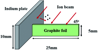
Commercially available graphite foil, which was cut into small pieces, 25 × 5 × 0.1 mm3, was used for the sample fabrication. Indium incorporated carbon nanofibers (In-CNFs) were grown at an edge of the foil. Fig. 1 shows a geometrical configuration of the graphite foil and an In plate (10 × 20 mm2), which were mounted on a water-cooled sample holder, for the growth of In-CNFs. The foil was placed perpendicularly with the In plate acting as an In supply source. The graphite foil edge and the In plate were co-irradiated with Ar+ ions at 1 keV and 600 eV for 60 minutes using Kaufman type ion gun (ION TECH. INC Ltd., model 3-1500-100FC) without any intentional sample heating. During the ion irradiation, a simultaneous supply of In onto the foil edge surface took place, resulting in the formation of In incorporated cones with a nanofiber (In-CNF) on the respective tips. Details of mechanism of the ion-induced amorphous CNFs has been explained in our previous works.22,24 The ion incidence angle was set to be 45° from the normal to the surface because an oblique Ar+ irradiation is known to be suitable for the formation of ion-induced CNFs.15,29 The beam diameter was about 60 mm. The basal and working pressures were 1.5 × 10⁻⁵ and 2 × 10⁻² Pa, respectively. After the ion irradiation, scanning electron microscope (SEM, JEOL JEM-5600) and transmission electron microscope (TEM, JEOL JEM-2010HR) were used for the observations of the surface morphologies and the crystallinity of the sample, respectively.3. Results and discussion
After Ar+ irradiation, the graphite foil at the position of 1.5 cm away from In plate was observed by SEM and TEM. Fig. 2 shows typical SEM images of In-CNF tipped cones after the ion irradiation. It should be noted that only a single nanofiber (In-CNF) grew on respective cones and no nanofiber grew without cone bases, similar to the previously reported pure and metal included CNFs.18,22–24,28,29 Both basal cones and In-CNFs pointed in the ion-beam direction. The CNFs were similar in length, 1.5–2.5 μm, for both surfaces, whereas the numerical density was much higher for the surface irradiated at 1 keV (∼6.8 × 103 mm−2) compared with that irradiated at 600 eV (∼3.3 × 103 mm−2). The growth mechanism of ion-induced CNFs is known to be explained in terms of the redeposition of sputter-ejected carbon atoms onto the ion-induced conical protrusions and the surface diffusion of the redeposited carbon atoms towards the cone tip to form CNFs.15,29 In the present case also, In would be included into ion-induced CNFs under the simultaneous In supply to form In-CNFs.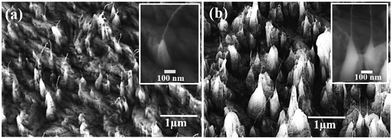 | ||
| Fig. 2 SEM images of the surfaces irradiated with Ar+ ions at (a) 600 eV and (b) 1 keV. Insets: Enlarged SEM images of typical CNF-tipped cones. | ||
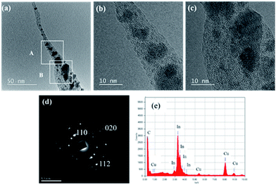
TEM images of a typical In-CNF tipped cone fabricated at 600 eV are shown in Fig. 3(a–c). Fig. 3(a) clearly shows that a fibrous structure grew on a tip of a cone. High-resolution TEM images of squares A (CNF bottom-stem part) and B (cone tip part) in Fig. 3(a) are shown in Fig. 3(b and c) which reveal no hollow structure and the amorphous nature of CNFs, respectively, disclosing that nanoparticles (nano-crystallites) of dark contrast were dispersed in the amorphous matrix. As shown in Fig. 3(d), the selected area electron diffraction (SAED) at around the cone tip part including A and B regions consisted of spotty rings corresponding to In (110), (020), and (112) lattice planes together with a weak broad ring of amorphous C. Thus, it is concluded that the nanofiber tipped cone consists of randomly oriented In nanocrystallites dispersed in amorphous C matrix. The composition of the In-CNF tipped cone was also confirmed by energy dispersive X-ray spectrometry (EDX), disclosing that no impurity was present (Fig. 3(e)).
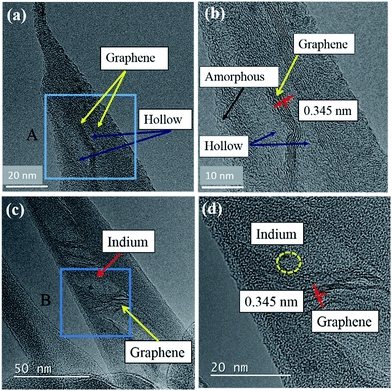
Fig. 4(a and c) show TEM images of typical In-CNF tipped cones fabricated at 1 keV. Fig. 4(b) shows high-magnification TEM image of region A of the fiber which is shown in Fig. 4(a). Similarly, Fig. 4(d) shows high magnification TEM image of region B of the fiber shown in Fig. 4(c). Both figures reveal the graphitized regions. It should be noted that the graphene region was always accompanied by hollow region. Examples of the hollow regions are indicated by arrows in Fig. 4(a–d). The graphene region seen in Fig. 4(b) is rather prominent and consisted of ∼6 straight layers, ∼30 nm in length with an inter-plane spacing of 0.345 nm corresponding to graphite (002) plane as reported for commercial graphene.9,10 As seen in Fig. 4(d), a tiny In nanoparticle was observed in some cones, and it also located in the vicinity of the hollow region. This point will be discussed later. The graphene and hollow regions were covered with amorphous C layers. It should be mentioned that the most of the In-CNF tipped cones fabricated at 1 keV was featured with this type of core–shell (graphitized core–amorphous shell) structures.
In the previous reports, we have demonstrated that many kinds of metals and semiconductors, such as Cu, Fe, Ag, Au, Co and Si, can be included into CNFs by simultaneously supplying them during Ar+ ion irradiation.22–24,28,29 They were always characterized by the CNF-tipped cone in shape and dispersion of metal or semiconductor nanoparticles in the amorphous carbon matrix in crystalline structure, namely no graphene formation, although most of them are well-known as catalysts for CVD graphene and CNT growth. In-CNF tipped cones demonstrated here are the only exception in crystalline nature. The formation of sp2 bonding is known to be thermodynamically favorable as compared to other forms of hybridization.1 This must imply that under a certain circumstance, where carbon atoms move (or displace) readily, sp2 bonding (namely graphene) tends to form naturally. In fact, it was demonstrated very recently that graphene can form even at the temperature as low as 250 °C using Sn, a low melting point (MP) metal catalyst by solid-liquid-solid phase reaction.27 Carbon atoms in molten metal would meet this condition. MP of bulk In is 156.6 °C, and it is also well-known that the smaller the particle size, the lower the MP. It is sometimes dramatic especially for the nanoparticles of less than 10 nm in size.30 As seen in Fig. 3(b and c), size of In particles included into the amorphous carbon matrix are less than 10 nm in average. Thus, MP of the included In nanoparticles would be much lower than that of the bulk In. So, In nanoparticles would have melted and moved to the base cone part in the case of Ar+ ion irradiation at 1 keV, whereas the temperature increase during ion irradiation was not so prominent at 600 eV. Thus, in the molten In, graphene would form. And this would be the reason why graphene layers were always accompanied with hollow regions and sometimes residual In nanoparticles located in the vicinity of hollow regions. In the present case, molten In nanoparticles are thought to catalyze the graphitization. In order to confirm this hypothesis and to estimate the necessary temperature for the graphene formation, thin In layer, 100 nm in thickness, and thin amorphous C layer, 50 nm in thickness, was deposited onto SiO2 covered Si substrates (In/C/SiO2/Si), and the thin film samples thus prepared were simply heated at 150 and 200 °C for 60 min under a vacuum condition of 10−3 Pa. In order to study the carbon state on the sample surface after heating, Raman analysis was performed.
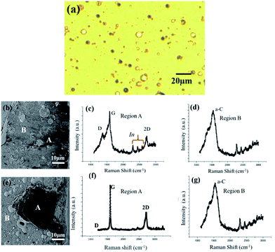
Fig. 5(a) shows a typical optical image of a sample surface before heating showing uniform film with some metal particles at some places. Fig. 5(b) presents a SEM image of sample surface after heating at 150 °C, disclosing that a flake of dark gray contrast (labeled A) is located on the surface after heating. Fig. 5(c and d) show Raman spectra attained at the flake (labeled A in Fig. 5(b)) and the surroundings (labeled B in Fig. 5(b)), respectively. It can be seen that the spectrum of region A consists of intense G and 2D peaks centered at 1583 and 2711 cm−1, respectively, with an intense D peak at 1354 cm−1, revealing the formation of multilayer graphene with defect. The peaks at 2260 and 2725 cm−1 are In peaks. Thus, from the Raman spectra it is concluded that the multilayer graphene formed on the In flake. By contrast, Raman spectrum of region B consisted of a broad peak at about 1550 cm−1, which is a typical amorphous carbon peak, together with In peaks at 2260 and 2725 cm−1, disclosing the amorphous carbon layer on the In film. Fig. 5(e–g) show a SEM image and Raman spectra for a thin film sample heated at 200 °C. As seen in Fig. 5(e), the surface morphology was similar to that of the 150 °C sample. However, a flake (labeled A) formed on the surface was much bigger than that of the 150 °C sample. It should be stressed that as seen in Fig. 5(f), the sharp and intense G and 2D peaks almost without D peak were detected for region A, clearly indicating the graphene formation of better quality than the 150 °C heated sample. Unfortunately, formed graphene did not cover the whole surface, but only on the In flake, as seen in Fig. 5(g) which discloses the amorphous C and In peaks for surrounding area B, similar to Fig. 5(d). Thus, it is concluded that by using In as a catalyst, graphene growth at the temperature as low as 150 °C is possible, and that higher quality graphene grows at elevated growth temperatures. We are now tackling the optimization of the layer thickness of In and C, and the direct graphene growth onto the flexible polymer substrates. The results will be dealt with forthcoming papers.
4. Conclusions
In summary, we demonstrated the graphene formation using indium as a catalyst for the samples of both room-temperature Ar+ irradiated carbon foil and In/carbon stacked films at 150 °C in the vacuum. The key of this low temperature graphene growth was the melting point of the catalyst metal. This finding will open up the synthesis of graphene at further lower temperatures.Conflicts of interest
There are no conflict of interest to declare.Notes and references
- A. K. Geim and K. S. Novoselov, Nat. Mater., 2007, 6, 183–191 CrossRef CAS PubMed.
- B. Dai, L. Fu, Z. Zou, M. Wang, H. Xu, S. Wang and Z. Liu, Nat. Commun., 2011, 2, 522 CrossRef PubMed.
- J.-J. Chen, J. Meng, D.-P. Yu and Z.-M. Liao, Sci. Rep., 2014, 4, 5065 CrossRef PubMed.
- J. Tesch, P. Leicht, F. Blumenschein, L. Gragnaniello, M. Fonin, L. E. Marsoner Steinkasserer, B. Paulus, E. Voloshina and Y. Dedkov, Sci. Rep., 2016, 6, 23439 CrossRef CAS PubMed.
- A. Naeemi and J. D. Meindl, IEEE Electron Device Lett., 2007, 28, 428–431 CrossRef CAS.
- W. Lv, Z. Li, Y. Deng, Q.-H. Yang and F. Kang, Energy Storage Mater., 2015, 2, 107–138 CrossRef.
- K. Chen, S. Song, F. Liu and D. Xue, Chem. Soc. Rev., 2015, 44, 6230–6257 RSC.
- X. Li, W. Cai, J. An, S. Kim, J. Nah, D. Yang, R. Piner, A. Velamakanni, I. Jung, E. Tutuc, S. K. Banerjee, L. Colombo and R. S. Ruoff, Science, 2009, 324, 1312–1314 CrossRef CAS PubMed.
- A. Reina, X. Jia, J. Ho, D. Nezich, H. Son, V. Bulovic, M. S. Dresselhaus and K. Jing, Nano Lett., 2009, 9, 30–35 CrossRef CAS PubMed.
- K. S. Kim, Y. Zhao, H. Jang, S. Y. Lee, J. M. Kim, K. S. Kim, J.-H. Ahn, P. Kim, J.-Y. Choi and B. H. Hong, Nature, 2009, 457, 706–710 CrossRef CAS PubMed.
- J. Kim, G. Lee and J. Kim, Appl. Phys. Lett., 2015, 107, 033104 CrossRef.
- M. Marchena, D. Janner, T. L. Chen, V. Finazzi and V. Pruneri, Opt. Mat. Express., 2016, 6, 3324–3334 Search PubMed.
- K. Sulaiman, A. Y. Ali, D. Elkington, K. Feron, K. F. Anderson, W. Belcher, P. Dastoor and X. Zhou, Carbon N. Y., 2016, 107, 325–331 CrossRef CAS.
- J. Jang, M. Son, S. Chung, K. Kim, C. Cho, B. H. Lee and M. Ham, Sci. Rep., 2015, 5, 17955 CrossRef CAS PubMed.
- M. Tanemura, T. Okita, H. Yamauchi, S. Tanemura and R. Morishima, Appl. Phys. Lett., 2004, 84, 3831–3833 CrossRef CAS.
- G. K. Wehner, J. Vac. Sci. Technol., A, 1985, 3, 1821–1835 CAS.
- P. Karmakar and D. Ghose, Surf. Sci., 2004, 554, L101–L106 CrossRef CAS.
- M. Tanemura, M. Kitazawa, J. Tanaka, T. Okita, R. Ohta, L. Miao and S. Tanemura, Jpn. J. Appl. Phys., 2006, 45, 2004–2008 CrossRef CAS.
- M. Tanemura, J. Tanaka, K. Itoh, Y. Fujimoto, Y. Agawa, L. Miao and S. Tanemura, Appl. Phys. Lett., 2005, 86, 1–3 CrossRef.
- P. Ghosh, M. Z. Yusop, D. Ghosh, A. Hayashi, Y. Hayashi and M. Tanemura, Chem. Commun., 2011, 47, 4820–4822 RSC.
- M. Kitazawa, R. Ohta, J. Tanaka and M. Tanemura, Jpn. J. Appl. Phys., 2007, 46, 5607–5610 CrossRef CAS.
- M. S. Rosmi, Y. Yaakob, M. Z. Mohd Yusop, S. Sharma, Z. Zulkifli, A. Supee, G. Kalita and M. Tanemura, AIP Adv., 2016, 6, 095109 CrossRef.
- M. Z. M. Yusop, P. Ghosh, Y. Yaakob, G. Kalita, M. Sasase, Y. Hayashi and M. Tanemura, ACS Nano., 2012, 6, 9567–9573 CrossRef CAS PubMed.
- Y. Yaakob, M. Z. Yusop, C. Takahashi, G. Kalita, P. Ghosh and M. Tanemura, Jpn. J. Appl. Phys., 2013, 52, 11NL01 CrossRef.
- M. S. Rosmi, M. Z. Yusop, G. Kalita, Y. Yaakob, C. Takahashi and M. Tanemura, Sci. Rep., 2014, 4, 7563 CrossRef CAS PubMed.
- M. S. Rosmi, Y. Yaakob, M. Z. Mohd Yusop, S. Sharma, R. Vishwakarma, M. Ibrahim, G. Kalita and M. Tanemura, RSC Adv., 2016, 6, 82459–82466 CAS.
- R. Vishwakarma, M. S. Rosmi, K. Takahashi, Y. Wakamatsu, Y. Yaakob, M. I. Araby, G. Kalita, M. Kitazawa and M. Tanemura, Sci. Rep., 2017, 7, 43756 CrossRef PubMed.
- Y. Sugita, M. Kitazawa, M. Zamri, M. Yusop, M. Tanemura, Y. Hayashi and R. Ohta, J. Vac. Sci. Technol. B., 2009, 27, 980 CAS.
- Y. Yaakob, Y. Kuwataka, M. Z. M. Yusop, S. Tanaka, M. S. Rosmi, G. Kalita and M. Tanemura, Phys. Status Solidi Basic Res., 2015, 252, 1345–1349 CrossRef CAS.
- M. Y. Efremov, F. Schiettekatte, M. Zhang, E. A. Olson, A. T. Kwan, R. S. Berry and L. H. Allen, Phys. Rev. Lett., 2000, 85, 3560–3563 CrossRef CAS PubMed.
| This journal is © The Royal Society of Chemistry 2017 |

