 Open Access Article
Creative Commons Attribution 3.0 Unported Licence
Tuning of the interval in a nanohole array of anodic porous alumina through deformation of polymer templates
T. Kondo *,
S. Nagao,
H. Miyazaki,
T. Yanagishita and
H. Masuda
Department of Applied Chemistry, Tokyo Metropolitan University, 1-1, Minamiosawa, Hachioji, Tokyo 192-0397, Japan. E-mail: kondo-toshiaki@tmu.ac.jp
First published on 19th September 2017
Abstract
A new type of process for the fabrication of ideally ordered anodic porous alumina with the desired hole interval based on the deformation of a polymer template and the subsequent formation of a metal mold is described. In this process, a pattern composed of an ordered array of concave structures is first prepared on a polymer sheet by imprinting using a starting metal (Ni) mold, and the interval in the pattern is tuned through the deformation of the polymer sheet. The Ni mold with the pattern having the tuned interval is formed by the electroplating of Ni using the polymer sheet as a template. Finally, the pretexturing of Al by imprinting using the obtained Ni mold and subsequent anodization generate ideally ordered anodic porous alumina with the desired hole interval.
1. Introduction
Anodic porous alumina, which is formed by the anodization of Al in an acidic electrolyte, has attracted considerable interest owing to its applicability to a wide range of scientific and technical fields based on its unique geometrical structures.1,2 To optimize the performance of the obtained devices, precise control of the geometrical structures of anodic porous alumina is an important issue to be resolved.3–13In our previous reports, we described a process that allows the formation of anodic porous alumina with an ideally ordered hole arrangement over the sample.14–19 In this process, a textured pattern composed of ordered concaves is formed by nanoimprinting Al using a mold with ordered convexes, and ideally ordered anodic porous alumina can be obtained by anodization of the textured Al at an appropriate voltage. Each concave in the pretextured pattern acts as an initiation site for hole development at the initial stage of anodization to generate an ideally ordered hole arrangement. The molds used for pretexturing by nanoimprinting are usually prepared by electron beam lithography (EBL).20 However, this technique has some drawbacks in the preparation of the molds: in addition to the requirement of expensive apparatus, it is a time-consuming process. In particular, in the case of preparing molds with fine patterns, a relatively long exposure time is required for the fabrication in addition to the need for precise setting of the fabrication conditions.
To overcome these problems, a new process for the preparation of molds for pretexturing is required. In the present report, we describe a new type of process for the preparation of molds with patterns having the desired intervals based on the deformation of polymer templates and its application to the formation of ideally ordered anodic porous alumina with the desired hole interval.
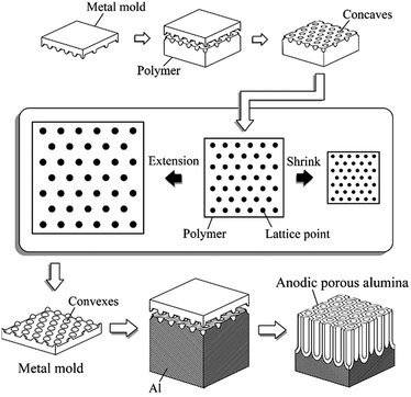
Fig. 1 schematically shows the tuning of the interval in the pattern on the mold and the hole interval in anodic porous alumina by the present process. In this process, a pattern composed of an ordered array of concaves is first prepared on a polymer sheet by imprinting using a starting metal (Ni) mold, and the interval in the pattern is modified through the deformation, i.e., extension or shrinkage, of the polymer sheet. The metal (Ni) mold with the pattern having the modified interval is obtained by the electroplating of Ni using the deformed polymer sheet as a template. The pretexturing of Al by nanoimprinting using the obtained Ni mold and the subsequent anodization generate ideally ordered anodic porous alumina with the modified hole interval. Although this process for modifying the interval in a nanoimprinted pattern on a heat shrink polymer has been reported,21 its application to the preparation of molds using a polymer sheet as a template has not yet been reported. The present process allows the fabrication of molds with patterns having desired intervals, and consequently anodic porous alumina with desired hole intervals. Therefore, it is expected to contribute to the high-throughput fabrication of ideally ordered anodic porous alumina, particularly specimens with reduced hole intervals.
2. Experimental
2.1 Increase in the hole interval in anodic porous alumina through extension process
Fig. 2 shows the fabrication process of a Ni mold with a modified pattern and ideally ordered anodic porous alumina with a modified hole interval. Fig. 2(a) illustrates the process for increasing the interval in the pattern on the mold and between the nanoholes in anodic porous alumina. This process is based on the deformation of the pattern by stretching a polymer sheet. A Ni mold prepared by EBL was pressed onto the surface of a polyethylene terephthalate (PET) sheet using oil-pressing apparatus equipped with a heater. The imprinting pressure was 157 MPa and the sheet was heated at 80 °C using a hot plate during imprinting. Then, the imprinted PET sheet was isotropically stretched mechanically in the planar direction while being heated at 200 °C using a heated air blower (HG2300EM, Steinel) during stretching. The PET sheet was stretched by a factor of 1.4, 1.6, or 2.0. To form an electroconductive layer for electroplating, a thin Ni layer was formed on the stretched PET sheet using an ion beam sputtering apparatus (South Bay Technology, Inc.). The thickness of this conductive layer was 30 nm. Then, Ni was electroplated on the PET sheet.20 By removing the PET sheet mechanically, the Ni mold was obtained. Next, the obtained Ni mold was pressed onto the surface of an Al plate by applying a pressure of 157 MPa at 150 °C. The textured Al plate was then anodized in 0.13 M citric acid solution at 16 °C for 10 min. The anodizing voltage was controlled from 280 to 400 V. After that, the anodic porous alumina was immersed in 5 wt% phosphoric acid solution at 30 °C for 1 h to increase the pore diameter.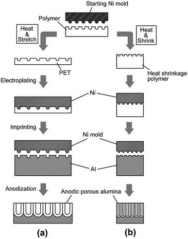 | ||
| Fig. 2 Fabrication process of ideally ordered anodic porous alumina with an adjusted hole interval through (a) extension and (b) shrinkage processes. | ||
2.2 Reduction in the hole interval in anodic porous alumina through shrinkage process
Fig. 2(b) shows the process used to reduce the interval in the pattern on the mold and anodic porous alumina. The reduction was carried out via the contribution of the pattern in the heat shrink polymer. In this process, the Ni mold was first pressed onto the surface of a heat shrink polymer (Grafix Shrink Film, Grafix Plastics)21 by applying a pressure of 274 MPa at room temperature. The imprinted polymer sheet was shrunk by heating at 200 °C for 3 min using the heated air blower. Ni was electroplated onto the shrunk polymer sheet to form a Ni mold. The obtained Ni mold was pressed onto an Al plate by applying a pressure of 196 MPa at 150 °C. The textured Al plate was anodized in 0.05 M oxalic acid solution at 16 °C by applying a voltage of 100 V for 40 s. For pore widening, the anodic porous alumina was immersed in 5 wt% phosphoric acid solution at 30 °C for 45 min.Repetition of the process described in Fig. 2(b) allows the further reduction of the pattern on the mold and in the anodic porous alumina. For example, a second reduction of the interval was carried out through the heat shrinkage of the polymer sheet at 200 °C for 3 min after imprinting at 274 MPa using the Ni mold obtained by the first reduction process. The Ni mold with the reduced pattern was obtained by electroplating using the shrunk polymer sheet. The obtained Ni mold was pressed on an Al plate by applying a pressure of 274 MPa. The anodization of Al was carried out in 0.05 M oxalic acid at 16 °C at 52 V for 40 s. The pore diameter was adjusted by dipping the sample in 5 wt% phosphoric acid at 30 °C for 30 min. The geometrical structures of the surface of the polymer and the anodic porous alumina were observed using a scanning electron microscope (SEM: JSM-6700F, JEOL).
3. Results and discussion
3.1 Increase in the hole interval in anodic porous alumina
Fig. 3 shows a SEM image of a typical Ni mold used as a starting structure. The interval and diameter of the convexes were 500 and 310 nm, respectively. The relative standard deviation (RSD) of the interval between the convexes was 1.3%.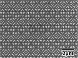 | ||
| Fig. 3 SEM image of the surface of a Ni mold used as a starting structure. The interval and diameter of the convexes were 500 and 310 nm, respectively. | ||
The left image of Fig. 4 shows a SEM image of the surface of the PET sheet after nanoimprinting using the Ni mold. An ordered array of concaves in a triangular lattice was observed. The interval and diameter of the concaves were 500 and 230 nm, respectively. The right image of Fig. 4 shows a SEM image of the surface of the PET sheet after isotropic stretching by a factor of 1.4 in the planar direction. From Fig. 4, it was confirmed that the textured nanopattern on the polymer sheet was maintained even after the stretching. The interval between the concaves was 700 nm, which was 1.4 times larger than the original interval. The enlargement factor of the interval between the concaves was in agreement with the degree of stretching of the PET sheet.
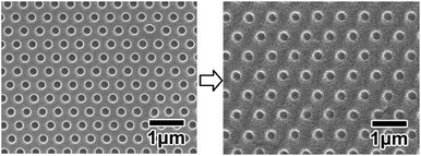 | ||
| Fig. 4 Imprinted PET sheet (left) before and (right) after the stretching process. The intervals between the concaves were 500 and 700 nm, respectively. | ||
Fig. 5(a) shows the Ni mold obtained by the electroplating of Ni using the stretched PET sheet as a template. The pretexturing of Al was carried out by using the obtained Ni mold for nanoimprinting. Then, the anodic porous alumina was obtained by anodization of the textured Al. Fig. 5(b) show a SEM image of the obtained anodic porous alumina. An ideally ordered nanohole array structure was confirmed. The interval and diameter of the nanoholes were 700 and 190 nm, respectively. The RSD of the hole interval was 2.7%.
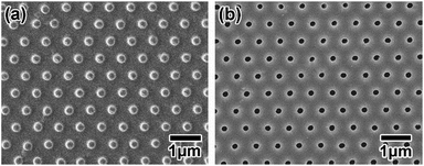 | ||
| Fig. 5 (a) Ni mold obtained by electroplating Ni on the stretched PET sheet. (b) Anodic porous alumina obtained by anodizing Al, on which ordered concaves were formed by the imprinting process using the Ni mold in Fig. 2(a). The intervals between the convexes and between the nanoholes were both 700 nm. | ||
The interval of the pattern in the Ni mold and the hole arrangement in the anodic porous alumina could be adjusted by varying the enlargement factor in the stretching of the PET sheet. Fig. 6 demonstrates the variation of the hole interval in anodic porous alumina obtained by this process. In the case of the samples in Fig. 6, the hole interval was adjusted to 800 nm (Fig. 6(a)) and 1000 nm (Fig. 6(b)). These structures were obtained with enlargement factors of the PET sheet of 1.6 and 2.0, respectively. The RSDs of the hole intervals were 2.2% (Fig. 6(a)) and 5.2% (Fig. 6(b)).
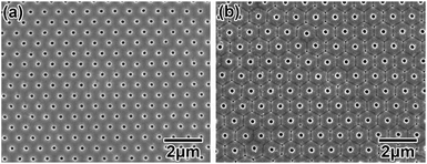 | ||
| Fig. 6 Anodic porous alumina with adjusted intervals between nanoholes obtained by stretching process. The intervals between the nanoholes were (a) 800 and (b) 1000 nm. | ||
3.2 Reduction in the hole interval in anodic porous alumina
The reduction of the interval in the Ni molds and the hole interval in the anodic porous alumina was carried out through the deformation of the pattern in the heat shrink polymer. Fig. 7 shows SEM images of a polymer sheet before and after shrinkage by heat treatment. The interval in the starting pattern was 500 nm, which was formed by imprinting using the Ni mold shown in Fig. 3. From Fig. 7, it was confirmed that the interval between the concaves in the polymer sheet was reduced from 500 to 250 nm through the shrinkage. The reduction rate was 50%, in good agreement with the shrinkage rate of the heat shrink film.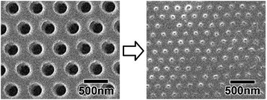 | ||
| Fig. 7 SEM images of heat shrink polymer (left) before and (right) after shrinkage by heat treatment. | ||
Using the polymer sheet with the reduced pattern as a template, a Ni mold with concaves having a reduced interval was obtained by electroplating (Fig. 8(a)), and anodic porous alumina with a reduced hole interval was then obtained (Fig. 8(b)) by using the obtained Ni mold for pretexturing. The RSD of the hole interval was 5.8%.
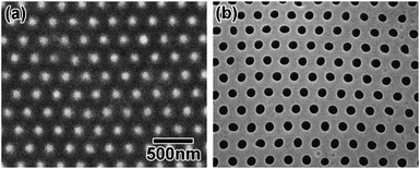 | ||
| Fig. 8 (a) Ni mold obtained using a shrunk polymer sheet as a template for electroplating. (b) Anodic porous alumina with reduced interval. | ||
3.3 Further reduction in the hole interval in anodic porous alumina
The repetition of the shrinkage process generated a further reduced polymer pattern, Ni mold, and anodic porous alumina with a hole array. Fig. 9(a) shows a SEM image of the polymer sheet after the two reduction processes. It was confirmed that the interval was reduced to 130 nm. This value was 25% of the initial interval in the starting structure. Fig. 9(b) shows the anodic porous alumina with the reduced pattern obtained by pretexturing using the metal mold produced from the polymer sheet. The RSD of the hole interval was 10%. Ideally ordered anodic porous alumina with a reduced hole interval was successfully obtained.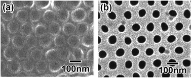 | ||
| Fig. 9 (a) Polymer sheet after second reduction process. (b) Anodic porous alumina with reduced hole interval obtained using the polymer sheet in (a). | ||
4. Conclusions
The interval in a pattern on a metal mold used for nanoimprinting was tuned through the deformation of a polymer template, and subsequent electroplating generated a metal mold with a modified pattern. For the modification of the polymer pattern, enlargement and shrinkage of the polymer sheet were successfully employed. Using the obtained Ni molds for the pretexturing of Al, ideally ordered anodic porous alumina with desired hole intervals was obtained. In addition, the repetition of the process allowed the further modification of the pattern. The present process is expected to be used for the high-throughput fabrication of ideally ordered anodic porous alumina with desired hole intervals and to contribute to extending the range of applications of ideally ordered anodic porous alumina.Conflicts of interest
There are no conflicts to declare.References
- G. E. Thompson, Thin Solid Films, 1997, 297, 192 CrossRef CAS.
- H. Masuda and K. Fukuda, Science, 1995, 268, 1466 CAS.
- I. Vlassiouk, A. Krasnoslobodtsev, S. Smirnov and M. Germann, Langmuir, 2004, 20, 9913 CrossRef CAS PubMed.
- F. Matsumoto, K. Nishio and H. Masuda, Adv. Mater., 2004, 16, 2105 CrossRef CAS.
- D.-L. Guo, L.-X. Fan, F.-H. Wang, S.-Y. Huang and X.-W. Zou, J. Phys. Chem. C, 2008, 112, 17952 CAS.
- J. P. Wu, I. W. M. Brown, M. E. Bowden and T. Kemmitt, Solid State Sci., 2010, 12, 1912 CrossRef CAS.
- K. Yasui, T. Morikawa, K. Nishio and H. Masuda, Jpn. J. Appl. Phys., Part 2, 2005, 44, L469 CrossRef CAS.
- H. Masuda, M. Ohya, K. Nishio, H. Asoh, M. Nakao, M. Nohtomi, A. Yokoo and T. Tamamura, Jpn. J. Appl. Phys., 2000, 39, L1039 CrossRef CAS.
- H. Masuda, M. Yamada, F. Matsumoto, S. Yokoyama, S. Mashiko, M. Nakao and K. Nishio, Adv. Mater., 2006, 18, 213 CrossRef CAS.
- T. Yanagishita, T. Kondo, K. Nishio and H. Masuda, J. Vac. Sci. Technol., B: Microelectron. Nanometer Struct.--Process., Meas., Phenom., 2008, 26, 1856 CAS.
- M. Nakao, S. Oku, T. Tamamura, K. Yasui and H. Masuda, Jpn. J. Appl. Phys., Part 1, 1999, 38, 1052 CrossRef CAS.
- H. Masuda, M. Watanabe, K. Yasui, D. Tryk, T. Rao and A. Fujishima, Adv. Mater., 2000, 12, 444 CrossRef CAS.
- T. Kondo, H. Masuda and K. Nishio, J. Phys. Chem. C, 2013, 117, 2531 CAS.
- H. Masuda, H. Yamada, M. Satoh, H. Asoh, M. Nakao and T. Tamamura, Appl. Phys. Lett., 1997, 71, 2770 CrossRef CAS.
- K. Nishio, T. Yanagishita, S. Hatakeyama, H. Maegawa and H. Masuda, J. Vac. Sci. Technol., B: Microelectron. Nanometer Struct.--Process., Meas., Phenom., 2008, 26, L10 CrossRef CAS.
- H. Masuda, K. Yasui, Y. Sakamoto, M. Nakao, T. Tamamura and K. Nishio, Jpn. J. Appl. Phys., 2001, 40, L1267 CrossRef CAS.
- Y. Matsui, K. Nishio and H. Masuda, Jpn. J. Appl. Phys., 2005, 44, 7726 CrossRef CAS.
- Y. Matsui, K. Nishio and H. Masuda, Small, 2006, 2, 522 CrossRef CAS PubMed.
- T. Kondo, S. Nagao, S. Hirano, T. Yanagishita, N. T. Nguyen, P. Schmuki and H. Masuda, Electrochem. Commun., 2016, 72, 100 CrossRef CAS.
- K. Yasui, K. Nishio, H. Nunokawa and H. Masuda, J. Vac. Sci. Technol., B: Microelectron. Nanometer Struct.--Process., Meas., Phenom., 2005, 23, L9 CrossRef CAS.
- A. Yokoo, K. Wada and L. C. Kimerling, Jpn. J. Appl. Phys., 2007, 46, 6395 CrossRef CAS.
| This journal is © The Royal Society of Chemistry 2017 |

