
 Open Access Article
 This Open Access Article is licensed under a
 Creative Commons Attribution 3.0 Unported Licence
Improved performance of hole-transporting layer-free perovskite solar cells by using graphene oxide sheets as the nucleation centers
Xue Sunab,
Tong Linab,
Qiaogang Songab,
Yue Fuab,
Ye Wangab,
Fangming Jina,
Haifeng Zhaoa,
Wenlian Lia,
Zisheng Su *a and
Bei Chua
*a and
Bei Chua
aState Key Laboratory of Luminescence and Applications, Changchun Institute of Optics, Fine Mechanics and Physics, Chinese Academy of Sciences, Changchun 130033, P. R. China. E-mail: suzs@ciomp.ac.cn; chub@ciomp.ac.cn
bUniversity of Chinese Academy of Sciences, Beijing, 100039, P. R. China
First published on 22nd September 2017
Abstract
Graphene oxide sheets (GOSs) are introduced between indium tin oxide (ITO) and CH3NH3PbI3 in inverted hole-transport layer-free planar heterojunction perovskite solar cells. The concentration of the GOSs is extremely low and they are sporadically covered on the ITO substrates. Combined with the high resistance of these GOSs, they cannot be regarded as an interface layer. However, the GOSs can act as the nucleation sites in the crystal growth process of CH3NH3PbI3 films, which results in dramatically improved morphology and crystallization of the CH3NH3PbI3 films. As a result, the performance of the devices is significantly improved as compared with the reference device. The optimized device shows a power conversion efficiency of 6.62%, which is about 40% higher than the reference devices. This improvement is attributed to the increased charge carrier transporting property and reduced charge carrier recombination in the CH3NH3PbI3 films.
Introduction
Lead-halide perovskite is used as a light absorber and holds great promise in the field of efficient and low-cost optoelectronic materials, owing to its extraordinary photonic and electronic properties. Perovskite solar cells (PSCs) have made impressive progress with power conversion efficiencies (PCEs) evolving from 3.8% to a certified 22.1% within just 8 years, and there is still room for growth.1–4 To boost the PCE, extensive research has been devoted to PSC devices, such as improving charge collection and transport efficiency, optimizing cell structure, and enhancing the quality of each layer.5–8 Perovskite solar cells have two types of cell structures: planar heterojunction and mesoscopic structure. Most of efficient mesoscopic PSCs employed meso-superstructure or condensed metal oxides such as TiO2 and Al2O3, and required high-temperature (500 °C) during the high-quality metal oxides produce processing, which is not suitable for fabricating on flexible plastic substrates.4,9–11 Relative to mesoporous PSCs, planar heterojunction devices have attracted much attention because of their simple structures and preparation process. Unfortunately, typical organic hole transport layers (HTLs) such as 2,2′,7,7′-tetrakis(N,N-di-p-methoxy phenylamine)-9,9-spirobi-fluorene (spiro-OMeTAD) and poly(3,4-ethylene dioxythiophene):poly(styrene sulfonate) (PEDOT:PSS) are expensive and may result in instability problems under ambient air.12 To overcome these disadvantages, researches on simplified structure like HTL-free have been put forward. Chen and co-workers fabricated inverted-structured HTL-free PSCs on flexible polyethylene terephthalate substrates, and a maximum PCE of 9.7% was obtained. At the same time, the structure of indium tin oxide (ITO)/CH3NH3PbI3/phenyl-C61-butyric acid methyl ester/Al without HTL achieved a PCE of 12.5%.13 Ye et al. spin-coated the hybrid precursor solution with both CuSCN and perovskite, and the device of ITO/MAPbI3−xClx (CuSCN)/C60/bathocuproine/Ag without HTL layer significantly accelerated hole transfer from the perovskite layer to ITO. The device reached a maximum PCE of 18.1%.14 Perovskite materials always exhibit high charge mobility, and therefore they are possible to be used as both absorb layer and HTL in order to achieve simple and low-cost HTL-free PSCs.15The interfacial energy structures and contact between the functional layers can directly affect the charge collection and extraction. Along with appropriate charge transport materials, it is vitally important for PSCs to have a light absorb layer with high crystallization and surface coverage. Many methods aimed to improve the film quality have been used, such as including additives into precursor, optimizing the film-fabrication methodology, improving composition, and perfecting the film-fabrication methodology.16 Liang et al. introduced 1,8-diiodooctane into perovskite precursor solution and effectively controlled the rate of perovskite crystallization.17 The growth of perovskite layer can also be manipulated by the insert of bottom nanoparticles18,19 and organic layers.20
Graphene and its derivatives, such as graphene oxide (GO) and reduced graphene oxide, are exploited as interfacial layers in PSCs. Owing to the GO chemical construction, oxygen atoms are usually more electronegative than carbon atoms. Thus, GO can be regarded as a p-doped material, and it has been inserted between perovskite and HTL (such as PEDOT:PSS and spiro-OMeTAD) or introduced as HTL into perovskite cell structures as reported.21–25 GO shows great potential in interface modification of perovskite solar cells.26 Therefore, the introduction of GO interface layers could effectively enhance charge extraction, improve energy alignment between interface layers and optimize perovskite crystallization. Graphene oxide sheets (GOSs) can be regard as 2D carbon–carbon structure like single-layer graphene sheets and contain various oxygen-containing functional groups (hydroxyl and epoxy groups) at its sheet edges. The abundant functional groups make GOSs have hydrophilic edges and hydrophobic centers, result in great dispersal stability, high surface energy, and amphiphilic function.23,27 These properties make them more suitable for application in PSCs, especially to control the crystal growth of the perovskite layers. In this work, GOSs are introduced to the ITO/CH3NH3PbI3 interface and improved morphology and crystalline are found for the CH3NH3PbI3 films. As the concentration of the GOSs is dramatically low, they cannot fully cover the ITO substrates. Combining with the high resistance of these GOSs,24,28 they cannot be regarded as an interface layer. As a result, the optimized HTL-free PSC reveals a PCE of 6.62%, which is about 40% improved compared with the reference device without GOSs.
Experimental
Device fabrication and characterization
The perovskite solar cells have a structure of ITO/GOSs/CH3NH3PbI3/C60/4,7-diphenyl-1,10-phenanthroline (Bphen)/Ag, as shown in Fig. 1(a). For reference, the device without GOSs was also fabricated. The energy level diagram of the devices is shown in Fig. 1(b) with the data cited from (ref. 29 and 30). The ITO substrates with a sheet resistance of 15 Ω sq−1 were routinely cleaned and UV-ozone treated as reported.30 The GOSs were dissolved in deionized water concentrations of 0.025, 0.05, and 0.1 mg ml−1, respectively. The solutions were ultrasonicated for 5 min and then filtered with a 0.45 μm filter before used. The GOSs solutions were spin-coated on the ITO substrates at 5000 rpm for 60 s in the atmosphere, and then annealed at 120 °C for 20 min. These substrates were then transferred to a N2 filled glove box to deposit CH3NH3PbI3 films. PbI2 and CH3NH3I with a mole ratio of 1![[thin space (1/6-em)]](https://www.rsc.org/images/entities/char_2009.gif) :1 were dissolved in a N,N-dimethylformamide (DMF) and dimethylsulfoxide (DMSO) mixed solution (volume ratio of 7:3), and then heated at 70 °C for 2 h to make sure they can be fully dissolved. The dissolved solution was spun on ITO substrates with or without GOSs at 2000 rpm for 60 s, and during the spin casting process the films were immediately exposed to 500 μl chlorobenzene at 20 s to induce fast crystallization. Then they were annealed at 70 °C for 1 min and 100 °C for 8 min. Finally, 50 nm C60, 5 nm Bphen, and 100 nm Ag were thermal evaporated in sequence in a vacuum chamber at a pressure of 5 × 10⁻⁴ Pa. Deposition rate and layer thickness were monitored in situ using oscillating quartz monitors. Evaporation rates were kept at 1 Å s−1 for C60 and Bphen, and 10 Å s−1 for Ag cathode. The device area is 0.09 cm2, determined by the overlap of the cathode and anode electrodes.
:1 were dissolved in a N,N-dimethylformamide (DMF) and dimethylsulfoxide (DMSO) mixed solution (volume ratio of 7:3), and then heated at 70 °C for 2 h to make sure they can be fully dissolved. The dissolved solution was spun on ITO substrates with or without GOSs at 2000 rpm for 60 s, and during the spin casting process the films were immediately exposed to 500 μl chlorobenzene at 20 s to induce fast crystallization. Then they were annealed at 70 °C for 1 min and 100 °C for 8 min. Finally, 50 nm C60, 5 nm Bphen, and 100 nm Ag were thermal evaporated in sequence in a vacuum chamber at a pressure of 5 × 10⁻⁴ Pa. Deposition rate and layer thickness were monitored in situ using oscillating quartz monitors. Evaporation rates were kept at 1 Å s−1 for C60 and Bphen, and 10 Å s−1 for Ag cathode. The device area is 0.09 cm2, determined by the overlap of the cathode and anode electrodes.
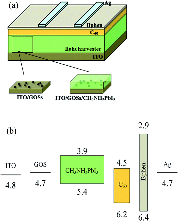 | ||
| Fig. 1 (a) Device structure and (b) the energy-level diagram of the perovskite solar cells. | ||
X-ray diffraction (XRD) patterns were measured with a Rigaku D/Max-2500 diffractometer using Cu Kα radiation (λ = 1.54 Å). Absorption spectra were recorded on a Shimadzu UV-3101PC spectrophotometer. Scanning electron microscopy (SEM) images were measured by a Hitachi S4800 field emission scanning electron microscopy. The surface topographies were imaged with a Bruker MultiMode 8 atomic force microscope (AFM) in tapping mode. Current–voltage (J–V) characteristics of the devices were measured with a Keithley 2400 source meter both in the dark and under illumination of an AM 1.5G solar simulator Newport, with an intensity of 100 mW cm−2. The voltage scans were swept from short circuit to forward bias with a rate of 0.05 V s−1. The IPCE spectra were performed with a Stanford SR803 lock-in amplifier under monochromatic illumination. All measurements were performed under ambient conditions.
Results and discussion
As the CH3NH3PbI3 films are deposited directly on the GOSs, the morphology of the GOSs on ITO substrates may have a significantly effect on the growth of the CH3NH3PbI3 films. However, no obviously difference is observed in the morphologies between the ITO substrates with and without GOSs from their SEM and AFM images. This may be attributed to the small size and thickness of these GOSs, which are much lower than the grain size and roughness of the ITO substrates. Thus Si wafers with a more smooth morphology are used as the substrates. The AFM images of GOSs with different concentrations on Si wafers are displayed in Fig. 2(a)–(d). The GOSs distributed separately on the substrates, and the density increases with the concentration of the GOSs. The mean diameter of the GOSs is about 60 nm and the thickness is about 2 nm. The large spacing between the GOSs makes sure that there is a large contact area between ITO and CH3NH3PbI3.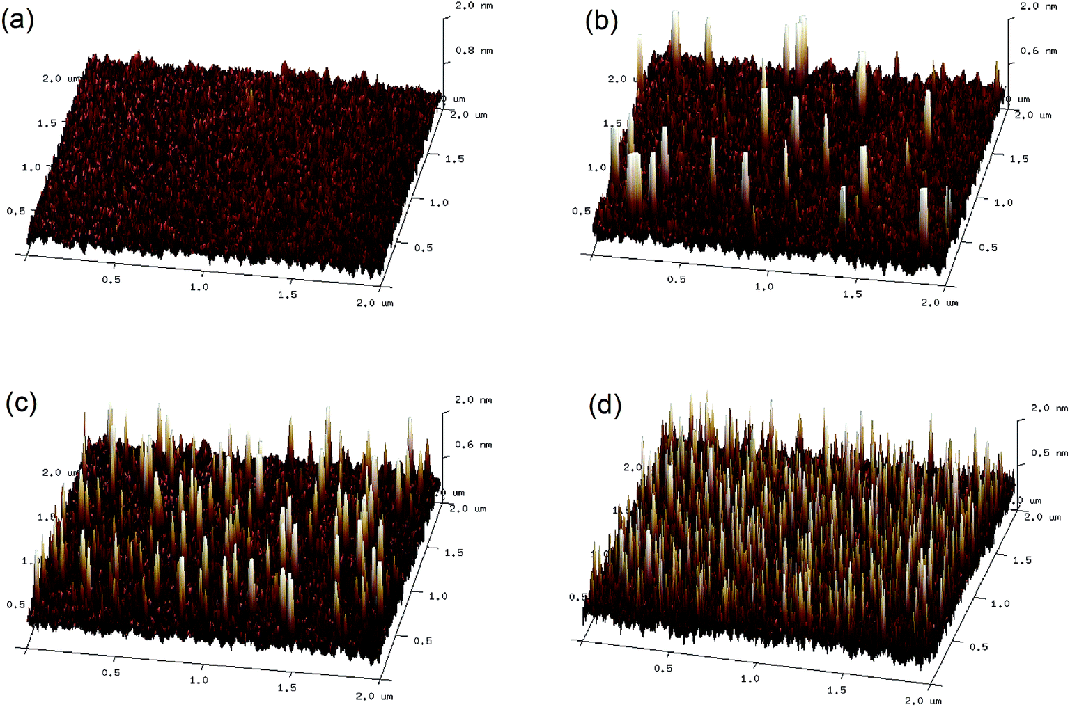 | ||
| Fig. 2 AFM images of (a) bare Si wafer and GOSs on Si wafers with concentrations of (b) 0.025, (c) 0.05, and (d) 0.1 mg ml−1. | ||
To evaluate the effects of the GOSs on the growth of the CH3NH3PbI3 films, the morphologies of CH3NH3PbI3 films are investigated. Fig. 3 shows the SEM images of the CH3NH3PbI3 films on ITO and GOSs coated ITO substrates. As expected, the morphologies of the CH3NH3PbI3 films are quite different when they are deposited on different substrates. CH3NH3PbI3 film on bare ITO exhibits a smooth and homogeneous morphology, but there are some small pinholes distributed on the film (Fig. 3a). The average grain size of this CH3NH3PbI3 film is about 200 nm. Compared with this film, the CH3NH3PbI3 films on GOSs show a more smooth, homogeneous, and pinhole-free morphology. Besides, the grains size is also dramatically increased, which is about twice of that on bare ITO substrate. It has been reported that the nucleation barrier is much lower in the heterogeneous nucleation at a liquid–solid interface than that in the homogeneous nucleation at a flat substrate. During the crystal growth process, the morphology and crystallization are sensitive to energy barrier of the reaction. The lower energy barrier results in the easier nucleation of CH3NH3PbI3 crystal.31 Such as when the precursor solution is deposited on mesoporous TiO2 scaffold, the crystallinity of perovskite becomes better compared with the crystal on a flat substate.32 The GOSs deposited on the ITO in this experiment is most likely to be regarded as the liquid–solid interface. The inhomogeneity effectively reduced energy barrier of nucleate, and the GOSs are functioned as effective nucleation sites, promoting the formation of CH3NH3PbI3 crystal, leading to a more preferential occurrence of large domains growing in these GOSs areas. Besides, it is reported that the element of O in the GOSs could combine with Pb in the CH3NH3PbI3 and creates Pb–O bond, which results in the improved crystal growth and passivated surface defects of the CH3NH3PbI3 films.20 These effects result in the larger grain size and higher crystalline of the CH3NH3PbI3 films on GOSs. However, when the concentration of GOSs is increased to 0.1 mg ml−1, the pinholes appear again. It has been reported that a higher density of the nucleation center will lead to the film morphology discrete and pin-holes appear.31 Thus the pinholes in the CH3NH3PbI3 film on 0.1 mg ml−1 GOSs may be attributed to the same mechanism.
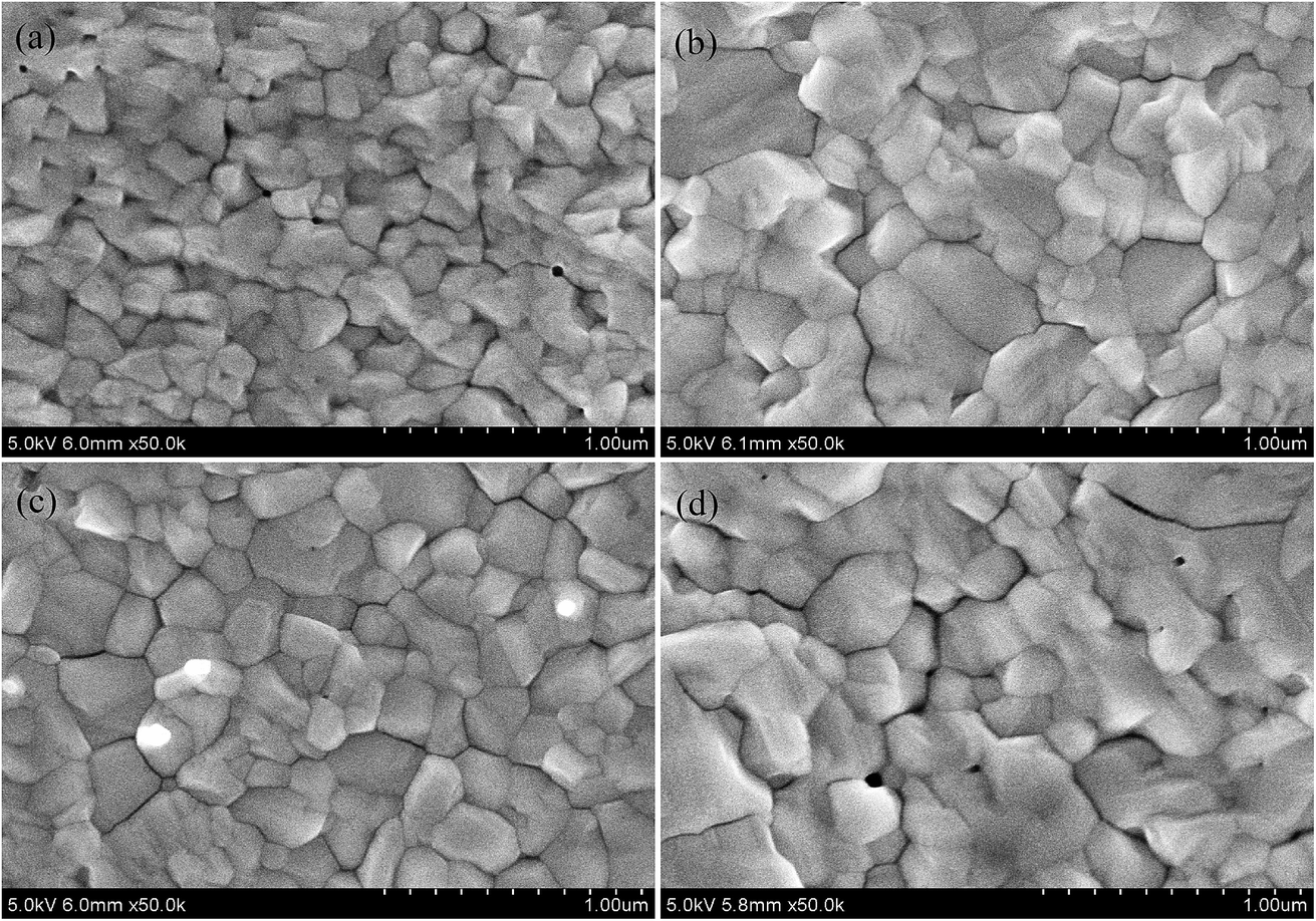 | ||
| Fig. 3 Top-view SEM images of the CH3NH3PbI3 films on (a) bare ITO, (b) 0.025, (c) 0.05, and (d) 0.1 mg ml−1 GOSs. | ||
In contrast, the GOSs have little effect on the thickness of the CH3NH3PbI3 films, which is all about 500 nm. Fig. 4 shows the cross-sectional SEM images of the CH3NH3PbI3 films on bare ITO and a typical one on GOSs. It is interesting to find that in the vertical direction the CH3NH3PbI3 film on bare ITO is consisted of several crystals. However, there are two distinct regions for the CH3NH3PbI3 film on GOSs, where one has the same structure to the CH3NH3PbI3 film on bare ITO (left side of Fig. 4a) and the other one has only one large crystal (right side of Fig. 4a). The difference should be attributed to their grown on different materials. The CH3NH3PbI3 crystal grown on GOSs may have a higher growth rate compared with that on ITO, which results in a larger CH3NH3PbI3 crystal size on GOSs. This also leads a little variation of the thickness of the CH3NH3PbI3 film on GOSs. These findings indicate that the grain size of CH3NH3PbI3 on GOSs is significant larger than that on bare ITO. The increased crystal particles results in the reduction of crystal boundaries (CBs). It is confirmed that crystal boundaries have higher surface potential, and the CBs generally lead to a downward bending of the energy band and hence retard the hole extraction.33 The reduction in total number of CBs could effectively reduce charge recombination in CH3NH3PbI3 films.
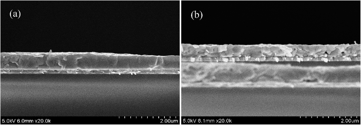 | ||
| Fig. 4 Cross-sectional SEM images of the CH3NH3PbI3 films on (a) GOSs and (b) bare ITO. | ||
For a further investigation of the GOSs effect on the CH3NH3PbI3 films, we analyzed the structural properties of the CH3NH3PbI3 films by XRD. The data was normalized and the curves are shown in Fig. 5. Sharp diffraction peaks at 2θ of 14.2° and 28.5° are observed in all the films with and without GOSs, which can be assigned to the (110) and (220) planes of the CH3NH3PbI3 crystal.34,35 The full width at half maximum (FWHM) of the diffraction peaks at 14.2° and 28.5° of the CH3NH3PbI3 films are listed in Table 1. The FWHMs of the diffraction peaks at 14.2° and 28.5° for the CH3NH3PbI3 films on bare ITO are 0.118° and 0.143°, respectively. However, they are reduced to less than 0.1° and 0.13° on GOSs, respectively. The narrowed FWHMs mean better crystallinity of CH3NH3PbI3 films on GOSs, which is consistent with the findings in SEM images.
 | ||
| Fig. 5 XRD patterns of the CH3NH3PbI3 films on (a) bare ITO, (b) 0.025, (c) 0.05, and (d) 0.1 mg ml−1 GOSs. | ||
| Concentration of GOSs (mg ml−1) | Full width at half maximum | |
|---|---|---|
| 14.2° | 28.5° | |
| W/O | 0.118° | 0.143° |
| 0.025 | 0.099° | 0.131° |
| 0.05 | 0.092° | 0.129° |
| 0.1 | 0.1° | 0.132° |
The CH3NH3PbI3 films show a broad absorption band in ultraviolet to visible region with an edge of about 780 nm (Fig. 6), corresponding to a bandgap of 1.59 eV. Although the CH3NH3PbI3 films with and without GOSs have dramatically different morphology and crystalline, they present almost the same absorption spectra. For comparison, we also show the absorption spectrum of the GOSs (0.1 mg ml−1) in Fig. 6. It means that the addition of GOSs has little influence on the total absorbance and the absorption is dominated by the CH3NH3PbI3 layer, which can be attributed to the lower absorption of GOSs in the visible region and the lower density of these GOSs on the substrates.
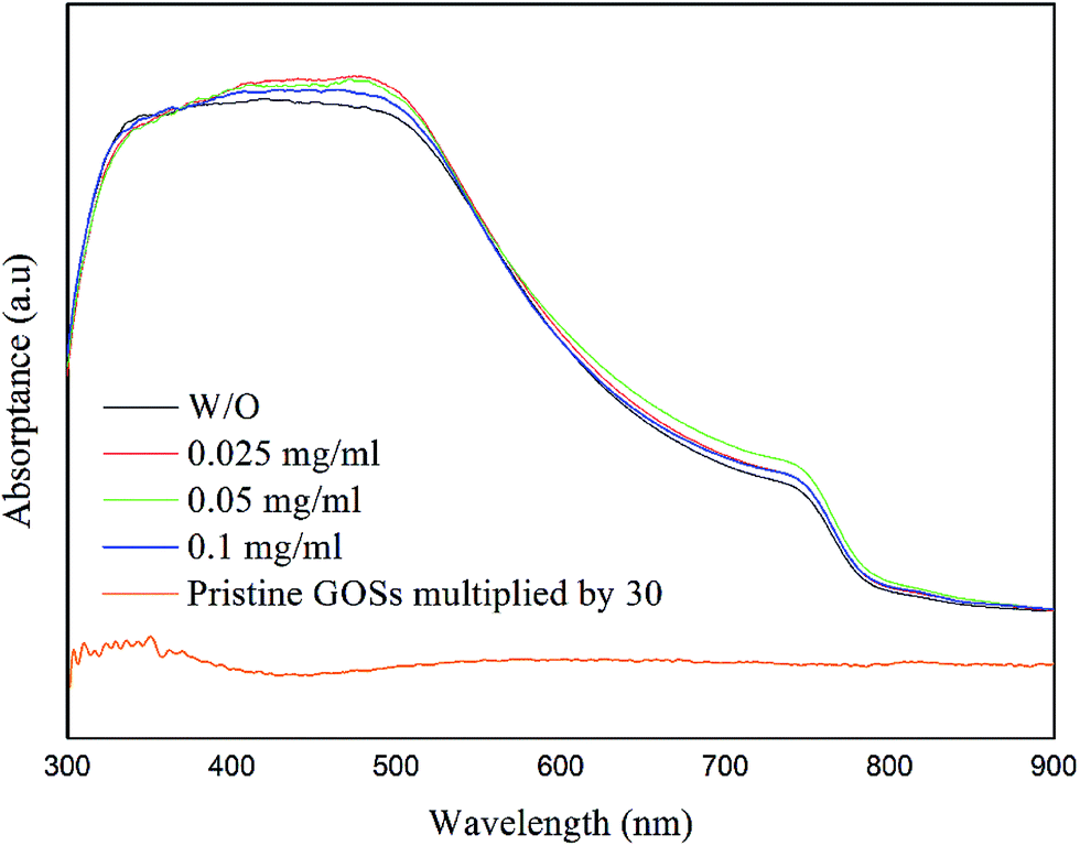 | ||
| Fig. 6 Absorbance spectra of the CH3NH3PbI3 films deposited on ITO with different concentrations of GOSs. The concentration of pristine GOSs in this figure is 0.1mg ml−1. | ||
In order to understand the effects of the GOSs on the performance of the devices, perovskite solar s with and without GOSs are fabricated. Fig. 7(a) shows the average J–V curves of perovskite solar cells and the detailed parameters extracted from the curves are summarized in Table 2. The reference device without GOSs shows an open-circuit voltage (VOC) of 0.91 V, short circuit current (JSC) of 12.15 mA cm−2, and fill-factor (FF) of 0.43, corresponding to a PCE of 4.78%. The performance of the devices is dramatically improved by introducing GOSs. Among the three devices, the device with 0.05 mg ml−1 GOSs exhibits the highest performance, which has a higher VOC of 0.94 V, JSC of 13.68 mA cm−2, FF of 0.52, and PCE of 6.62%. This suggests that the PCE is improved of about 40% as compared with the reference device. As the devices have almost the same absorption spectra, the improved performance cannot be assigned to the improved absorption efficiency. Thus the improvement can only be attributed to the increased charge carrier transporting property and collection efficiency, which is related to the anode/perovskite interface and/or the bulk properties of the perovskite layer.6–8 The work function of GOS is 4.7 eV,29 which is comparable to that of ITO of 4.8 eV.30 This rules out the increased work function to the improved performance of the devices. GOSs usually have large resistance,28 thus the holes are difficult to be extracted via these GOSs and then collected by ITO electrode. This is also the reason that the performance is reduced for the device with a higher concentration of GOSs. From the AFM images, it can be found that the density of GOSs on ITO substrates is low, which insures high contact areas between ITO and CH3NH3PbI3. As a result, holes can be direct collected by the ITO anode. In view of this, the devices with GOSs can also be regarded as HTL-free perovskite solar cells, and the improved performance of these devices can be attributed to the improved morphology and crystalline and hence increased charge carrier transporting property and reduced charge carrier recombination in the CH3NH3PbI3 films.
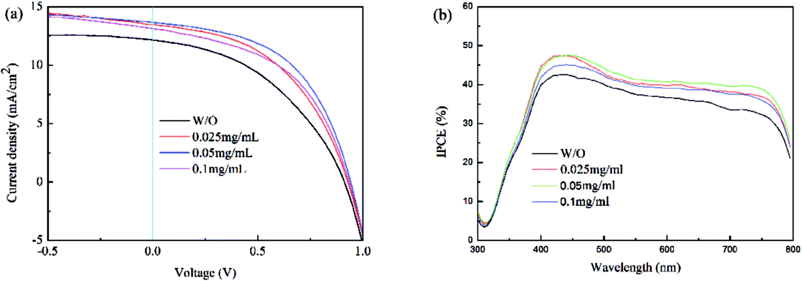 | ||
| Fig. 7 (a) J–V curves and (b) IPCE spectra of the devices with different concentrations of GOSs on ITO substrates. | ||
Fig. 7(b) shows the average IPCE spectra of the devices. It is obvious that the samples show broad response at 400–800 nm. The responses of the devices with GOSs are higher than that of the reference device in the whole response region, which is consistent with the JSC found in the J–V curves. The calculated JSC from these IPCE spectra are also listed in Table 2, and it can be found that these data are well agree with the ones extracted from J–V curves. Moreover, the champion device with 0.05 mg ml−1 GOSs exhibits a PCE of 7.03%, VOC of 0.94 V, JSC of 14.21 mA cm−2, FF of 0.56. Similarly, the JSC calculated from the IPCE spectrum of this device is 13.75 mA cm−2, which is also comparable to the data extracted from the J–V curve.
Conclusion
In summary, HTL-free inverted planar heterojunction perovskite solar cells are demonstrated. By inserting small amount of GOSs between ITO and CH3NH3PbI3, the morphology and crystallization of the CH3NH3PbI3 films are dramatically improved, which is attributed that the GOSs provide nucleation centers in the process of CH3NH3PbI3 crystal growth. As a result, a 40% increased PCE of the optimized device is observed compared with the reference device. These findings indicate that the properties of the perovskite films can be manipulated by well controlling the crystal growth process, and this strategy may have the potential application in other type perovskite optoelectronic devices.Conflicts of interest
There are no conflicts to declare.Acknowledgements
This work was supported by the National Natural Science Foundation of China (61575192, 61604149, 61376062, and 61376022), the Science and Technology Development Plan of Jilin Province (20170520130JH), and the project of Jiangsu Key Laboratory for Carbon-Based Functional Materials and Devices (KJS1615).References
- D. Y. Lee, S. I. Na and S. S. Kim, Nanoscale, 2016, 8, 1513–1522 RSC.
- W. S. Yang, J. H. Noh, N. J. Jeon, Y. C. Kim, S. Ryu, J. Seo and S. I. Seok, Science, 2015, 348, 1234–1237 CrossRef CAS PubMed.
- C. Y. Kuang, G. Tang, T. G. Jiu, H. Yang, H. B. Liu, B. R. Li, W. N. Luo, X. D. Li, W. J. Zhang, F. S. Lu, J. F. Fang and Y. L. Li, Nano Lett., 2015, 15, 2756–2762 CrossRef CAS PubMed.
- J. Burschka, N. Pellet, S. J. Moon, R. Humphry-Baker, P. Gao, M. K. Nazeeruddin and M. Gratzel, Nature, 2013, 499, 316–319 CrossRef CAS PubMed.
- P. M. Da and G. F. Zheng, Nano Res., 2017, 10, 1471–1497 CrossRef CAS.
- F. Dong, Y. Guo, P. Xu, X. Yin, Y. Li and M. He, Sci. China Mater., 2017, 60, 295–303 CrossRef.
- X. Yin, Z. Xu, Y. Guo, P. Xu and M. He, ACS Appl. Mater. Interfaces, 2016, 8, 29580–29587 CAS.
- X. Yin, Y. J. Guo, Z. S. Xue, P. Xu, M. He and B. Liu, Nano Res., 2015, 8, 1997–2003 CrossRef CAS.
- M. Saliba, S. Orlandi, T. Matsui, S. Aghazada, M. Cavazzini, J. P. Correa-Baena, P. Gao, R. Scopelliti, E. Mosconi, K. H. Dahmen, F. De Angelis, A. Abate, A. Hagfeldt, G. Pozzi, M. Graetzel and M. K. Nazeeruddin, Nat. Energy, 2016, 1, 15017 CrossRef CAS.
- N. J. Jeon, J. H. Noh, Y. C. Kim, W. S. Yang, S. Ryu and S. Il Seol, Nat. Mater., 2014, 13, 897–903 CrossRef CAS PubMed.
- H. S. Kim, C. R. Lee, J. H. Im, K. B. Lee, T. Moehl, A. Marchioro, S. J. Moon, R. Humphry-Baker, J. H. Yum, J. E. Moser, M. Gratzel and N. G. Park, Sci. Rep., 2012, 2, 591 CrossRef PubMed.
- T. Leijtens, G. E. Eperon, S. Pathak, A. Abate, M. M. Lee and H. J. Snaith, Nat. Commun., 2013, 4, 2885 Search PubMed.
- Y. Zhang, X. T. Hu, L. Chen, Z. Q. Huang, Q. X. Fu, Y. W. Liu, L. Zhang and Y. W. Chen, Org. Electron., 2016, 30, 281–288 CrossRef CAS.
- S. Ye, H. Rao, W. Yan, Y. Li, W. Sun, H. Peng, Z. Liu, Z. Bian, Y. Li and C. Huang, Adv. Mater., 2016, 28, 9648–9654 CrossRef CAS PubMed.
- M. Gratzel, Nat. Mater., 2014, 13, 838–842 CrossRef CAS PubMed.
- B. Yang, O. Dyck, J. Poplawsky, J. Keum, A. Puretzky, S. Das, I. Ivanov, C. Rouleau, G. Duscher, D. Geohegan and K. Xiao, J. Am. Chem. Soc., 2015, 137, 9210–9213 CrossRef CAS PubMed.
- P. W. Liang, C. Y. Liao, C. C. Chueh, F. Zuo, S. T. Williams, X. K. Xin, J. J. Lin and A. K. Y. Jen, Adv. Mater., 2014, 26, 3748–3754 CrossRef CAS PubMed.
- Z. K. Wang, M. Li, D. X. Yuan, X. B. Shi, H. Ma and L. S. Liao, ACS Appl. Mater. Interfaces, 2015, 7, 9645–9651 CAS.
- L. Liu, Q. Y. Xi, G. Gao, W. Yang, H. Zhou, Y. X. Zhao, C. Q. Wu, L. D. Wang and J. W. Xu, Sol. Energy Mater. Sol. Cells, 2016, 157, 937–942 CrossRef CAS.
- Z. K. Wang, X. Gong, M. Li, Y. Hu, J. M. Wang, H. Ma and L. S. Liao, ACS Nano, 2016, 10, 5479–5489 CrossRef CAS PubMed.
- Y. Long, K. Wang, G. L. Xiang, K. Song, G. Zhou and X. Wang, Adv. Mater., 2017, 29, 1606093 CrossRef PubMed.
- H. Luo, X. H. Lin, X. Hou, L. K. Pan, S. M. Huang and X. H. Chen, Nano–Micro Lett., 2017, 9, 319 Search PubMed.
- W. Z. Li, H. P. Dong, X. D. Guo, N. Li, J. W. Li, G. D. Niu and L. D. Wang, J. Mater. Chem. A, 2014, 2, 20105–20111 CAS.
- J. S. Yeo, R. Kang, S. Lee, Y. J. Jeon, N. Myoung, C. L. Lee, D. Y. Kim, J. M. Yun, Y. H. Seo, S. S. Kim and S. I. Na, Nano Energy, 2015, 12, 96–104 CrossRef CAS.
- Z. W. Wu, S. Bai, J. Xiang, Z. C. Yuan, Y. G. Yang, W. Cui, X. Y. Gao, Z. Liu, Y. Z. Jin and B. Q. Sun, Nanoscale, 2014, 6, 10505–10510 RSC.
- A. Giuri, S. A. Masi, S. Colella, A. Kovtun, S. Dell'Elce, E. Treossi, A. Liscio, C. E. Corcione, A. Rizzo and A. Listorti, Adv. Funct. Mater., 2016, 26, 6985–6994 CrossRef CAS.
- K. P. Loh, Q. L. Bao, G. Eda and M. Chhowalla, Nat. Chem., 2010, 2, 1015–1024 CrossRef CAS PubMed.
- J. M. Yun, J. S. Yeo, J. Kim, H. G. Jeong, D. Y. Kim, Y. J. Noh, S. S. Kim, B. C. Ku and S. I. Na, Adv. Mater., 2011, 23, 4923–4928 CrossRef CAS PubMed.
- J. Kim, H. Lee, S. J. Lee, W. J. da Silva, A. B. Yusoff and J. Jang, J. Mater. Chem. A, 2015, 3, 22035–22042 CAS.
- F. H. Hou, Z. S. Su, F. M. Jin, X. W. Yan, L. D. Wang, H. F. Zhao, J. Z. Zhu, B. Chu and W. L. Li, Nanoscale, 2015, 7, 9427–9432 RSC.
- S. S. Li, C. H. Chang, Y. C. Wang, C. W. Lin, D. Y. Wang, J. C. Lin, C. C. Chen, H. S. Sheu, H. C. Chia, W. R. Wu, U. S. Jeng, C. T. Liang, R. Sankar, F. C. Chou and C. W. Chen, Energy Environ. Sci., 2016, 9, 1282–1289 CAS.
- T. A. Berhe, W. N. Su, C. H. Chen, C. J. Pan, J. H. Cheng, H. M. Chen, M. C. Tsai, L. Y. Chen, A. A. Dubale and B. J. Hwang, Energy Environ. Sci., 2016, 9, 323–356 CAS.
- Q. Chen, H. P. Zhou, T. B. Song, S. Luo, Z. R. Hong, H. S. Duan, L. T. Dou, Y. S. Liu and Y. Yang, Nano Lett., 2014, 14, 4158–4163 CrossRef CAS PubMed.
- M. Liu, M. B. Johnston and H. J. Snaith, Nature, 2013, 501, 395–398 CrossRef CAS PubMed.
- J. Kim, M. A. Mat Teridi, A. R. Mohd Yusoff and J. Jang, Sci. Rep., 2016, 6, 27773 CrossRef CAS PubMed.
| This journal is © The Royal Society of Chemistry 2017 |