 Open Access Article
Improving the performance and stability of flexible pressure sensors with an air gap structure†
Xiongbang Wei *a,
Lun Xiaoa,
Wen Huangb,
Jiaxuan Liaoc and
Zhi David Chen
 ad
ad
aSchool of Optoelectronic Information, University of Electronic Science and Technology of China, Chengdu, 610054, China. E-mail: weixiongbang@uestc.edu.cn
bState Key Laboratory of Electronic Thin Films and Integrated Devices, University of Electronic Science and Technology of China, Chengdu 610054, China
cSchool of Energy Science and Engineering, University of Electronic Science and Technology of China, Chengdu, 610054, China
dDepartment of Electrical & Computer Engineering, Center for Nanoscale Science & Engineering, University of Kentucky, Lexington, Kentucky 40506, USA
First published on 16th October 2017
Abstract
A highly sensitive flexible resistive pressure sensor based on an air gap structure was presented. The flexible pressure sensor consists of two face to face polydimethylsiloxane (PDMS) films covered with carbon nanotubes (CNTs). The pressure sensor with a 230 μm thickness air gap has relatively high sensitivity (58.9 kPa−1 in the range of 1–5 Pa, 0.66 kPa−1 in the range of 5–100 Pa), low detectable pressure limit (1 Pa), and a short response time (less than 1 s). The test results showed that the pressure sensor with an appropriate air gap has excellent pressure sensitive performance and application potential.
1. Introduction
In the past few years, significant progress has been achieved for flexible pressure sensors because of their unique applications in touch screens,1,2 medical diagnosis,3–5 smart robotics,6,7 and microsurgery.8 Considerable progress has been made to-date in the design of “skin-like” sensors, including that based on resistive,3,5,9 capacitive,10,11 OFET,7,12 piezoelectric,8,13,14 and triboelectric15,16 principles. Among them, the resistance-type pressure sensors were predominantly used due to their small low detectable pressure limit and high reproducibility.4,5,17,18 Also, compared with other pressure sensors, resistance-type sensors have the advantages of much simpler mechanism, easier fabrication, easier measurement, and more extensive research and application.19Carbon nanotube (CNT) has proven unprecedented performance in flexible electronic devices due to their excellent chemical and physical properties, such as remarkable mechanical flexibility, tunable metallic/semiconducting properties, and high optical transmittance.20–23 Based on this, much effort has been devoted to studying of CNT for stretchable flexible devices during the past few years. In prior studies, the flexible resistance-type pressure sensors based on the individual carbon nanotubes(CNTs) or composite materials with dispersed CNTs showed good stretchability and sensitivity.4,7,12,14–26 Sensitivity of this flexible resistive pressure sensor is greatly dependent on the resistive change of CNTs. However, the piezoresistive materials without deformable structures under external pressure often limit the sensitivity in response to low detectable pressures. Hence, the performance of the flexible resistive pressure sensor could be improved by adjusting the feature of microstructures or through the introduction of smart 3-D microstructures.3,4,13,14,27–29 Soonjae et al. fabricated a piezoresistive CNT-polymer-composite-based tactile sensor, and observed a sensitivity of 6.67%/N for the maximum force up to 2 N.27 Yilmazoglu et al. studied a structure that integrated flexible, vertically aligned MWCNT arrays between flat carbon nanotube electrodes. Due to the flexible structure of the microsized 3D aligned CNTs, good piezoresistivity with decrease of resistance up to ∼35% at 32 mN of the MWCNT arrays was observed.30 Their results indicated that their CNT structures can be utilized for tactile sensing components, and confirmed the feasibility of accessing and utilizing nanoscopic CNT bundles via lithographic processing.30 Fan found that flexible sensors with pyramid-shaped microstructures have high sensitivity and the low detection limit, comparing with the cube-featured sensors and line-featured sensors.9 Zhang et al. have developed a novel method for the fabrication of tactile sensor by combining uniform micro-patterned polydimethylsiloxane (PDMS) films with CNTs. By virtue of the microstructures deformation of PDMS under pressure, the tactile sensor showed a sensitivity of 1.8 kPa−1 at 200 Pa.4
In prior work, we present a highly sensitive flexible tactile sensor based on microstructured multi-wall carbon nanotube (MWCNT) arrays with patterned cross-contacted electrodes and acquired good results. The sensor unit was constructed through a sandwich structure comprising the microstructured MWCNT/PDMS film and patterned Au/Ni/PET film.31 Also, a capacitance-type flexible sensor was investigated and demonstrated that the flexible pressure sensor constructed with two layers of microstructured AgNWs/PDMS films exhibits high sensitivity (1.1 kPa−1) and low detection limit of 1 Pa.32 Herein, an easy-fabricated flexible resistance-type pressure sensor with air gap as the microstructure was presented. A pair of strip-shaped bare PDMS films were inserted between two PDMS films, which covered with CNTs, to form an air gap microstructure. To evaluate the effect of the air gap, a traditional sensor without any microstructure and a sensor using micro-patterned PDMS film were assembled and tested for comparison. Based on our tests, the as-prepared flexible pressure sensor with a 230 μm thick air gap exhibits high sensitivity and the low detection limit (1 Pa). The sensitivity of this kind of pressure sensors can reach 58.9 kPa−1 in the low pressure region (1–5 Pa) and 0.66 kPa−1 in the high pressure region (5–100 Pa). The response time of the pressure sensor is less than 1s. In addition, the performance of the pressure sensor with air gap is more stable due to the support of PDMS strips.
2. Experimental
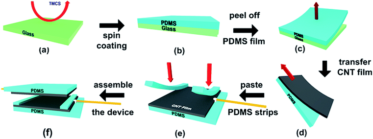
In our design, CNTs prepared by vacuum filtration method was transferred onto PDMS thick film to fabricate the flexible conducting film. The flat glass sheet and the ground glass sheet were used as the molds for the flat PDMS film and the micro-patterned PDMS film respectively. In order to facilitate subsequent peeling of PDMS film from the glass sheet, the glass sheet needed hydrophobic pretreatment before spin coating process. For pretreatment, the glass sheet was first soaked in concentrated sulfuric acid and hydrogen peroxide (30 wt%) for 30 min respectively. Immediately following washed by DI water, the glass sheet was blown dry with nitrogen. Then, the glass sheet was treated in the trimethylchlorosilane (TMCS) vapor bath at 75 °C for half an hour (Fig. 1a) and then the organic groups were introduced on the glass surface.For fabrication of the PDMS thick film, PDMS mixture of base and cross-linker (Dow Corning Sylgard 184; the weight ratio of base to cross linker was 10![[thin space (1/6-em)]](https://www.rsc.org/images/entities/char_2009.gif) :
:![[thin space (1/6-em)]](https://www.rsc.org/images/entities/char_2009.gif) 1) was stirred for 20 min and degassed in vacuum for 30 min at room temperature. Then the PDMS mixture was spin-coated onto the flat glass sheet at the speed of 500 rpm for 60 s (Fig. 1b). After solidified at 75 °C for 1 h, the uniform PDMS film was peeled off from the glass sheet (Fig. 1c).
1) was stirred for 20 min and degassed in vacuum for 30 min at room temperature. Then the PDMS mixture was spin-coated onto the flat glass sheet at the speed of 500 rpm for 60 s (Fig. 1b). After solidified at 75 °C for 1 h, the uniform PDMS film was peeled off from the glass sheet (Fig. 1c).
To make the PDMS film conductive, free-standing CNTs were synthesized by the vacuum filtration method reported.31 For transferring the free-standing CNTs onto the surface of the PDMS film, the glass sheet with PDMS film attached was immersed into the deionized water with free-standing CNTs floating on water surface. The glass sheet was lifted gradually to pick up the CNTs and make it attached the PDMS film (Fig. 1d). Finally, the conducting film was annealed in air at 100 °C for 30 min to improve its stability.
As shown in Fig. 2, all flexible pressure sensors designed were built with two face to face CNT/PDMS conducting films. A pair of Ag electrode were placed on the edge of each conducting film with copper test wire connected. Four structures of flexible pressure sensors were designed, a traditional sensor without any microstructure on CNT/PDMS conducting film (named as T-PS), a sensor using micro-patterned CNT/PDMS conducting film (named as P-PS), a sensor with a pair of strip-shaped bare PDMS inserted between the two face to face CNT/PDMS conducting films to form a thin air gap (named as OLS-PS), and a sensor with two pairs of strip-shaped bare PDMS inserted between the two face to face CNT/PDMS conducting films to form a thick air gap (named as TLS-PS). PDMS films prepared with smooth flat glass showed smooth surface. However, as using ground glass as template, PDMS films prepared showed microstructure surface (see Fig. S1 in the ESI†). The flat PDMS films of three structures, T-PS, OLS-PS, and TLS-PS, were prepared on flat glass sheet, and micro-patterned PDMS film of P-PS was prepared on ground glass sheet.
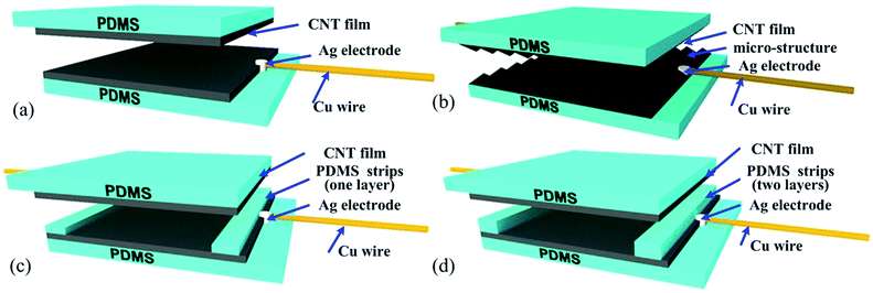 | ||
| Fig. 2 Structures of four flexible pressure sensors. (a) T-PS structure, (b) P-PS structure, (c) OLS-PS structure, (d) TLS-PS structure. | ||
To assemble the T-PS, two face to face CNT/PDMS conducting films were stagger contact with each other and the Ag electrode does not touch the surface of the other film (Fig. 2a). The micro-patterned CNT/PDMS conducting film of the P-PS were fabricated by the ground glass as mask, and the P-PS was assembled in the same way as T-PS (Fig. 2b). Based on the traditional structure, a pair of PDMS strips (30 mm long, 3 mm wide, and 230 μm thick) were pasted along the opposite edges of CNT/PDMS conducting films and assembled face to face (Fig. 1e, f and 2c). Similarly, to assemble the TLS-PS, two lays of PDMS strips (30 mm long, 3 mm wide, and 460 μm thick) were pasted along the edges of CNT/PDMS conducting films and assembled alike (Fig. 2d).
3. Results and discussion
For flexible pressure sensors, the low detectable pressure limit (named as LDPL), the sensitivity (defined by S = δ(ΔR/R0)/δP, where ΔR is the resistance change upon applied pressure of P, and R0 is the initial resistance without applied pressure) and the response time are very important parameters.Fig. 3 shows the response curves of the prepared flexible pressure sensors under their LDPL. LDPL values and the resistance change ratio (under LDPL) of the corresponding pressure sensor were noted in the figures. The T-PS has 3 Pa LDPL value and the resistance change ratio (ΔR/R) of the pressure sensor can reach 5.1% (Fig. 3a). The OLS-PS has a minimum value of LDPL (1 Pa) among these pressure sensors and its resistance change ratio can reach 16.2% (Fig. 3b). Although the TLS-PS has the largest resistance change ratio (35.7%) under its LDPL, the LDPL value of the TLS-PS is maximum (5 Pa) among these sensors (Fig. 3c). The results revealed that the pressure sensors with air gap have larger resistance change ratio. It can be attributed to the designed air gaps, which enable the upper CNT/PDMS conducting film to have larger deformation under certain pressure. The results showed that CNT film prepared by filtration is composed of many independent CNT fibers, and the length of CNT fiber is about 5–10 μm, and the diameter is about 50–60 nm (ESI, Fig. S2†). Therefore, larger deformation can generate a larger variation of contact area between the two conducting films, leading to a larger resistance change ratio. So OLS-PS has a larger resistance change ratio than T-PS, and TLS-PS has the maximum ratio. Because the air gap structure can separate the upper conducting film from bottom conducting film with a small contact area, sensor with an appropriate air gap thickness can reduce the LPDL. When the pressure sensor is loaded with a testing pressure, the upper conducting film will bend down and reduce the resistance value of the pressure sensor. However, too large air gap cannot make the pressure sensor generate enough deformation to change the resistance value due to no changing the contact area between two conducting films under too small testing pressure. Therefore, the LDPL value of the TLS-PS (5 Pa) is larger than that of OLS-PS (1 Pa).
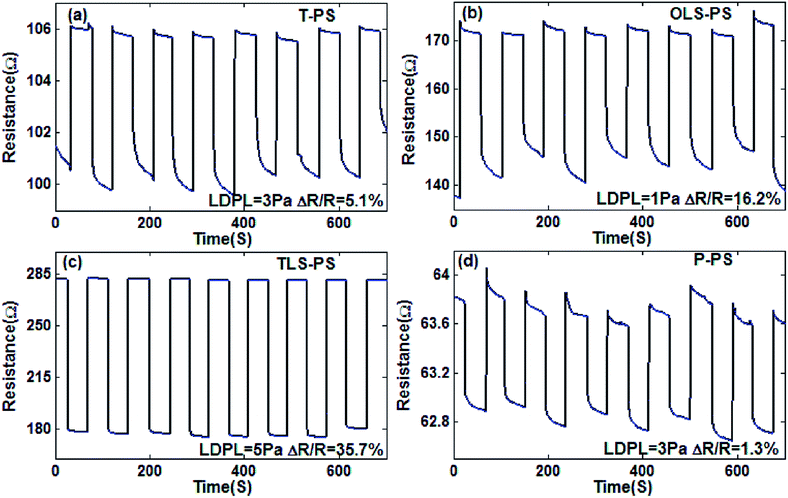 | ||
| Fig. 3 Response curves of four structural pressure sensors under their LDPL. (a) T-PS under 3 Pa, (b) OLS-PS under 1 Pa, (c) TLS-PS under 5 Pa, (d) P-PS under 3 Pa. | ||
Fig. 3d shows that the P-PS has the same LDPL (3 pa) as the T-PS, but the P-PS has the a very small resistance change ratio, which is only 1.3%. The response curves also show that the performance of the P-PS is not very stable. The poor properties of the P-PS are caused by the unstable surface morphology of the flexible patterned conducting film. The surface of CNT/PDMS films prepared using the flat glass as templates only showed small protuberance structure (about 50 nm height), and without large scale microstructure. The small protuberance structure on the surface of CNT/PDMS film is attributed to the contraction of the CNT film. Also, it can be observed that the CNT binds tightly to PDMS film substrate. (ESI, Fig. S3(a)†). However, as using ground glass as template, PDMS films prepared showed microstructure surface, microstructural CNT/PDMS film can be successfully prepared. The protuberance structure of CNT/PDMS film prepared is of micro scale with a width of about 3 μm and a height of about 5 μm. Due to the large size of the microstructure, the CNT film is difficult to overcome its internal stress, which eventually leads to the CNT and PDMS film substrate not closely bonded. (ESI, Fig. S3(b)†). The stability test showed that the appropriate thickness of the air gap structure can significantly improve the responsivity, sensitivity and stability of the device. Of the four structures response performance of the pressure sensors with air gaps (OLS-PS and TLS-PS) are more stable, which can be verified from the sensors' response curves. (ESI, Fig. S4(b)†). Because the bare PDMS strips can support the upper conducting film and avoid the collapse of the upper conducting film, response curves exhibit excellent stability. This mechanism improves the stability of pressure sensors and leads to a short response time of the OLS-PS and the TLS-PS samples (less than 1 s). So, the air gap structure, can effectively decrease the LDPL and enhance the resistance change ratio of the pressure sensors under low pressure, and the bare PDMS strips could improve the pressure sensor stability. Raman test results have showed that the CNT films are composed of carbon nanotubes, and the impurities of the films are very few (see Fig. S5, S6, and Table S1 in the ESI†).
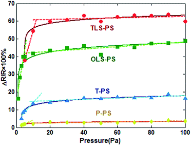
The resistance change ratio of the four pressure sensors was plotted as a function of the applied pressure, as shown in Fig. 4. As the dash line in Fig. 4 shown, there are two linear regions separated by a turning point for every sensor measurement. The slope of the liner region equal to the sensitivity of pressure sensors in the fixed pressure range. The curve has a large slope under the low pressure and a small slope under the high pressure.
That the resistance response curves have two linear regions is caused by reasons as follows. For all these four sensors, there is a space between the two conducting films of devices. Therefore, in the low pressure region, deformation of the flexible conducting films changes markedly when the applied pressure increases. Different deformation could generate different contact areas between the two conducting films. A small increase in the contact area could cause a sharp decrease in resistance. Then, quickly decrease of the pressure sensors' resistance result in extremely high sensitivity. However, in the high pressure region, the contact area between the conducting layers is almost same when the applied pressure continues to increase. When the applied pressure exceeding the tolerance limit of the conducting films, the upper conducting film are fully in contact with the bottom conducting film. In this case, the larger pressure in the large pressure region can only make the upper conducting film contact more closely with bottom conducting film, leading to less and less sensitivity.
Sensitivities of the pressure sensors in different regions were calculated. As the Fig. 4 showed, the OLS-PS has the maximum sensitivity (58.9 kPa−1 in 1–5 Pa; 0.66 kPa−1 in 5–100 Pa) in both the low pressure region and the high pressure region. And the sensitivity of TLS-PS (33.40 kPa−1 in 5–10 Pa; 0.25 kPa−1 in 10–100 Pa) is higher than that of the T-PS (10.69 kPa−1 in 3–10 Pa; 0.36 kPa−1 in 10–100 Pa), but lower than that of the OLS-PS. Table S2 (in the ESI†) shows the sensitivities of different pressure sensors in different regions. When there is no pressure applied on the pressure sensor, the PDMS strip can separate the upper conducting film from the bottom conducting film, resulting in a small initial contact area between the two films. When a low pressure is applied on the upper PDMS film, the upper conducting film bends down and the contact area between two conducting films increases, leading to a sharp decrease of sensor's resistance. So the pressure sensor with the air gap has larger sensitivity. The simulation results basically match our testing results (see Fig. S7 in the ESI†). However, too little pressure cannot make the upper conducting film to generate enough deformation to change the contact area between two conducting films if the air gap is too thick. Therefore, the TLS-PS has a smaller sensitivity and a larger LDPL compared with the OLS-PS. The resistance change ratio of the TLS-PS is largest because the thicker air gap can generate a larger resistance change ratio in the high pressure region. Different from the pressure sensor with air gap, the T-PS usually has a crevice between two conducting films after the device is assembled. But the crevice has not enough space for the upper conducting film to generate a large deformation. So the contact area change in the T-PS is smaller than the pressure sensor with an air gap, leading to a small resistance change and low sensitivity.
The pressure sensors with micro-structures should have higher sensitivity and lower LDPL compared with the T-PS,4,10,13,33 however, the P-PS has a low sensitivity (4.00 kPa−1 in 3–4 Pa; 0.14 kPa−1 in 5–10 Pa) and a small resistance change ratio (1.3%) in our experiments. This can be attributed to the difference that, in the P-PS, CNTs film cannot fit the large aspect ratio surface of the micro-patterned PDMS film perfectly, and the micro-structure on the patterned PDMS couldn't function well.
Fig. 5 illustrates the application of OLS-PS on monitoring the motion of a human hand, where a flexible pressure sensor was pasted on the back of a person's hand. The Keithley 2700 was connected to the pressure sensor to obtain the resistance value variation. When the person kept changing gesture from “making a fist” to “opening palm”, a clear pulse in resistance response curve was observed, and the resistance change ratio can reach 30%. All in all, the pressure sensor can detect the motion of a human hand, and thus it has potential applications in smart robotics.
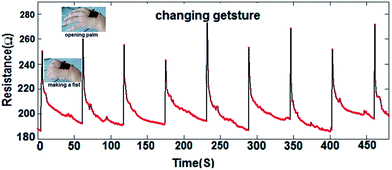 | ||
| Fig. 5 The resistance response curve of monitoring the tester's gesture from “making a fist” to “opening palm”. | ||
4. Conclusions
In conclusion, we demonstrated a highly sensitive flexible pressure sensor based on the air gap structure. The pressure sensor with 230 μm thickness air gap has a relatively higher sensitivity (58.9 kPa−1 in the range of 1–5 Pa, 0.66 kPa−1 in the range of 5–100 Pa), a lower LDPL (1 Pa), and a shorter response time (less than 1 s). The results showed that the air gap structure can be applied to the resistance-type pressure sensor to improve its performance. The flexible pressure sensor based on the air gap structure not only has the advantages of simple structure and stable performance, but also has excellent pressure sensitive performance and application potential.Conflicts of interest
There are no conflicts to declare.Acknowledgements
This work was supported by the grants from the National Natural Science Foundation of China under Grant No. 61474016, 61405026, 61405025, and National Basic Research Program of China (973 Program) under Grant No. 2015CB351905.Notes and references
- M. S. Noh, S. Kim, D. K. Hwang and C. Y. Kang, Sens. Actuators, A, 2017, 261, 288 CrossRef CAS.
- P. Sahatiya and S. Badhulika, RSC Adv., 2016, 6, 95836 RSC.
- Y.-K. Fuh, Po-C. Chen, H.-C. Ho, Z.-M. Huang and S.-C. Li, RSC Adv., 2015, 5, 67787 RSC.
- X. Wang, Y. Gu, Z. Xiong, Z. Cui and T. Zhang, Adv. Mater., 2014, 26, 1336 CrossRef CAS PubMed.
- S. Gong, W. Schwalb, Y. Wang, Y. Chen, Y. Tang, J. Si, B. Shirinzadeh and W. Cheng, Nat. Commun., 2014, 5, 3132 Search PubMed.
- S. Jung, J. H. Kim, J. Kim, S. Choi, J. Lee, I. Park, T. Hyeon and D. H. Kim, Adv. Mater., 2014, 26, 4825 CrossRef CAS PubMed.
- D. J. Lipomi, M. Vosgueritchian, B. C. Tee, S. L. Hellstrom, J. A. Lee, C. H. Fox and Z. Bao, Nat. Nanotechnol., 2011, 6, 788 CrossRef CAS PubMed.
- S. Sokhanvar, M. Packirisamy and J. Dargahi, Smart Mater. Struct., 2007, 16, 989 CrossRef CAS.
- F. R. Fan, L. Lin, G. Zhu, W. Wu, R. Zhang and Z. L. Wang, Nano Lett., 2012, 12, 3109 CrossRef CAS PubMed.
- J. J. Boland, Nat. Mater., 2010, 9, 790 CrossRef CAS PubMed.
- S. Baek, H. Jang, S. Y. Kim, H. Jeong, S. Han, Y. Jang, D. H. Kim and H. S. Lee, RSC Adv., 2017, 7, 39420 RSC.
- G. Schwartz, B. C. Tee, J. Mei, A. L. Appleton, D. H. Kim, H. Wang and Z. Bao, Nat. Commun., 2013, 4, 1859 CrossRef PubMed.
- J. Wang, H. Sato, C. Xu and M. Taya, J. Appl. Phys., 2009, 105, 083515 CrossRef.
- W. Choi, J. Lee, Y. Kyoung Yoo, S. Kang, J. Kim and H. Lee, Appl. Phys. Lett., 2014, 104, 123701 CrossRef.
- K. N. Kim, J. P. Lee, S.-H. Lee, S. C. Lee and J. M. Baik, RSC Adv., 2016, 6, 88526 RSC.
- D. Kim, H. Moon Lee and Y.-K. Choi, RSC Adv., 2017, 7, 137 RSC.
- C. L. Choong, M. B. Shim, B. S. Lee, S. Jeon, D. S. Ko, T. H. Kang, J. Bae, S. H. Lee, K. E. Byun, J. Im, Y. J. Jeong, C. E. Park, J. J. Park and U. I. Chung, Adv. Mater., 2014, 26, 3451 CrossRef CAS PubMed.
- M. Kumar and H. Bhaskaran, Nano Lett., 2015, 15, 2562 CrossRef CAS PubMed.
- N. N. Jason, M. D. Ho and W. Cheng, J. Mater. Chem. C, 2017, 5, 5845 RSC.
- X. W. Wang, Z. Liu and T. Zhang, Small, 2017, 13, 1602790 CrossRef PubMed.
- P. Lv, K. H. Yu, X. W. Tan, R. L. Zheng, Y. W. Ni, Z. Y. Wang, C. X. Liu and W. Wei, RSC Adv., 2016, 6, 11256 RSC.
- Y. Li, H. Zhang, Y. G. Yao, T. T. Li, Y. Y. Zhang, Q. W. Li and Z. D. Dai, RSC Adv., 2015, 5, 46749 RSC.
- A. K. Geim and K. S. Novoselov, Nat. Mater., 2007, 6, 183 CrossRef CAS PubMed.
- T. Sekitani, Y. Noguchi, K. Hata, T. Fukushima, T. Aida and T. Someya, Science, 2008, 321, 1468 CrossRef CAS PubMed.
- K. Lee, S. S. Lee, J. A. Lee, K. C. Lee and S. Ji, Appl. Phys. Lett., 2010, 96, 013511 CrossRef.
- S. Park, M. Vosguerichian and Z. Bao, Nanoscale, 2013, 5, 1727 RSC.
- S. Pyo, J.-I. Lee, M.-O. Kim, T. Chung, O. Yongkeun, S.-C. Lim, J. Park and J. Kim, J. Micromech. Microeng., 2014, 24, 075012 CrossRef.
- C. F. Hu, W.-S. Su and W. Fang, J. Micromech. Microeng., 2011, 21, 115012 CrossRef.
- C. F. Hu, J. Y. Wang, Y. C. Liu, M. H. Tsai and W. Fang, Nanotechnology, 2013, 24, 444006 CrossRef PubMed.
- O. Yilmazoglu, A. Popp, D. Pavlidis, J. J. Schneider, D. Garth, F. Schuttler and G. Battenberg, Nanotechnology, 2012, 23, 085501 CrossRef CAS PubMed.
- X. Li, W. Huang, G. Yao, M. Gao, X. B. Wei, Z. W. Liu, H. Zhang, T. X. Gong and B. Yu, Scr. Mater., 2017, 129, 61 CrossRef CAS.
- Y. Quan, X. B. Wei, L. Xiao, T. Wu, H. Y. Pang, T. F. Liu, W. Huang, S. H. Wu, S. B. Li and Z. Chen, J. Alloys Compd., 2017, 699, 824 CrossRef CAS.
- X. Wang, G. Li, R. Liu, H. Ding and T. Zhang, J. Mater. Chem., 2012, 22, 21824 RSC.
Footnote |
| † Electronic supplementary information (ESI) available: Details of the samples' SEM images, Raman spectra, stability response diagram. See DOI: 10.1039/c7ra09392f |
| This journal is © The Royal Society of Chemistry 2017 |

