 Open Access Article
Creative Commons Attribution 3.0 Unported Licence
The large-area preparation and photoelectrochemical properties of graphene/ZnO nanorod composite film
Hongyan Wu *a,
Xingming Zhaoa,
Jianliang Lib and
Songtao Dongc
aJiangsu Key Laboratory for Optoelectronic Detection of Atmosphere and Ocean, School of Physics & Optoelectronic Engineering, Nanjing University of Information Science & Technology, Nanjing, China. E-mail: wuhy2009@nuist.edu.cn; 13260815003@163.com
bCollege of Material Science and Technology, Nanjing University of Science and Technology, Nanjing, China. E-mail: jianliangli@163.com
cInstitute of Material Science and Engineering, Jiangsu University of Science and Technology, Zhenjiang, China. E-mail: stdong@just.edn.cn
First published on 8th December 2017
Abstract
We proposed a new method for preparing a single-crystalline (002)-oriented ZnO nanorod (ZnONR) array and graphene/ZnO nanorod (GZN) composite film on quartz plates using double glow plasma surface alloying (DGPSA) technology. The effects of graphene film on the photoelectrochemical properties of ZnO thin film were investigated. Ultraviolet (UV)-visible spectroscopy showed that the total transmittance of the GZN composite film was maintained at nearly 75% and the addition of graphene caused an increase in the absorption intensity at wavelengths greater than 375 nm. The contact angle (51°) of the GZN film after UV irradiation was lower than that (82.4°) of the film before UV irradiation. A comparison of the photoelectrochemical properties of graphene, ZnO and GZN films indicated that the synergistic effects of graphene and the ZnONR array enhanced charge transfer on the surface and reduced impedance in the solid state interface layer. In other words, the introduction of graphene has an obvious influence on the photoelectrochemical properties of GZN composite film. Therefore, our study suggests for the first time that double-glow plasma surface treatment can be considered as a new potential technology for the large-area preparation of graphene and GZN composite film.
Background
ZnO, with a direct wide bandgap (∼3.4 eV) and large exciton binding energy (60 meV), has been widely used in optoelectronic devices, e.g. UV nanolasers,1 photodetectors,2 field-effect transistors,3 and photovoltaic devices.4–6 However, single ZnO film has low interfacial charge-transfer efficiency and a high recombination rate of photo-generated electrons and holes. Recently, ZnO-based hybrid nanostructures with 2D nanomaterials have been attracting more attention, since 2D carbon nanostructures, as conductive carbon mats, anchor metal oxide materials to form new nanocomposite hybrid materials with potential applications in optoelectronics and energy conversion devices. Graphene, as a single layer of 2D-honeycomb carbon atoms, is one of the most hotly studied materials.7–9 Owing to its fascinating physical properties, e.g. high electrical conductivity, ultrahigh mobility and high transparency,10–14 graphene has been successfully modified with various ZnO nanostructures for high-efficiency photovoltaic devices,15–17 highly sensitive flexible sensors,18,19 solar water splitting20 and supercapacitors.21,22 Furthermore, research has demonstrated that the incorporation of graphene into ZnO nanostructures will provide synergistic effects in light absorption and electron transport.23 It has been reported that graphene/ZnO composite films have potential applications in dye sensitized solar cells (DSSCs) and UV photoelectrochemical detection devices.24,25 In view of application to DSSCs, the combination of graphene and semiconductors (i.e., ZnO and TiO2) can provide a large receptor interface, which is beneficial for electron injection into semiconductors, improving the conversion efficiency of solar cells. Moreover, graphene can also enhance the adsorption of dye molecules on the photoanode. For UV detection, the incorporation of graphene into ZnO nanostructures enhances charge transfer and the separation rate of photoinduced charges, which can improve the sensitivity for UV photoelectrochemical detection. For example, Kang Z. et al. showed a self-powered, UV-activated photoelectrochemical biosensor based on a vertical ZnO nanorod (NR) array directly synthesized on graphene through hydrothermal methods; the rGO/ZnONR array provided a robust approach for the UV photoelectrochemical detection of biomolecules.26 In recent years, many studies have reported the fabrication of ZnONR films via sol–gel or magnetron sputtering methods. Simultaneously, the growth of graphene was mainly performed via chemical deposition, epitaxial growth or self-assembly techniques and Hummers' method.27,28 In view of conventional synthesis methods for ZnO, Nie29 proposed that poly(methyl methacrylate) (PMMA)-supported monolayer graphene film could be transferred onto the surface of a ZnONR array and the PMMA could then be removed with acetone solution. The major obstacle in these methods is that graphene directly transferred onto the surface of ZnO film is not suitable for the large-area fabrication of composite films, and there is poor adhesion between the graphene and the ZnO film. A comparative study of ZnO film, graphene film and ZnO/graphene composite film is provided in Table 1.| Material | Preparation method | Optical–electrical performance | Limitations | Applications | Reference |
|---|---|---|---|---|---|
| ZnO film | Hydrothermal methods | High electron mobility (196 cm2 V−1 s−1) | Low efficiency of interfacial charge transfer (∼10−16 cm4 s−1) | UV nanolasers | 1–6 |
| Chemical vapor deposition | Large exciton binding energy (60 meV) | High recombination rate of photogenerated electrons and holes | Field-effect transistors | ||
| Electrochemical deposition | High internal photoconductive gain (∼41 A W−1) | UV sensors | |||
| Magnetron sputtering | Photovoltaic devices | ||||
| Graphene film | Chemical vapor deposition | Ultrahigh carrier mobility (1.5 × 104 cm2 V−1 s−1) | Low adhesion with the substrate | UV sensors | 27 and 28 |
| Hummers' method | Ultrahigh light transmittance (∼97.7%) | Limited preparation methods on an arbitrary substrate | Photovoltaic devices | ||
| Supercapacitors | |||||
| ZnO/graphene film | Electrochemical deposition | Ultrahigh responsitivity and photoconductive gain (∼113 A W−1) | — | UV sensors | 24–26 and 29 |
| Hydrothermal methods | High efficiency of interfacial charge transfer | Photovoltaic devices | |||
| Transfer methods | High separation rate of photoinduced charges | Solar water splitting |
However, few studies involve the large-area preparation of graphene/ZnO nanorod (GZN) composite film, using plasma surface technology, for application in various photodetector devices. Comparing with other glow discharge techniques, the double-glow plasma surface alloying (DGPSA) technique is a novel surface modification method, which involves a double-glow plasma discharge and can provide the ability to enhance the sputtering yield. One of the major advantages of DGPSA technology is that strong adhesion between the coating and the substrate can be obtained.
Herein, we firstly propose a novel method for preparing transparent GZN composite film on a quartz substrate through a simple two-step process for ZnONRs and graphene film, using the DGPSA technique. The composition, morphology and microstructure were characterized using Raman spectroscopy, atomic force microscopy (AFM), scanning electron microscopy (SEM) and X-ray photoelectron spectroscopy (XPS). UV-induced photosensitivity measurements were collected using UV-visible spectroscopy, and water contact angles and electrochemical impedance spectra (EIS) were collected for samples exposed and unexposed to UV irradiation. The research aims to confirm that GZN composite film prepared using DGPSA shows effective transmission of photogenerated electrons, and can act as an alternative photoanode material in solar cells and UV photoelectrochemical devices.
Experimental methods
Synthesis of GZN composite film
Experiments were performed in a double glow plasma surface metallurgy device. A schematic diagram of the device used in this study is shown in Fig. 1(a). There was double glow discharge in the vacuum chamber. Three electrodes were fixed in the chamber, one anode and two negatively charged members. There was one glow discharge as the work-piece electrode heated the substrate to a high temperature and a second glow discharge as the source electrode provided the desired deposition material. The hollow cathode effect was used to improve the sputtering density of the double-glow plasma.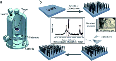 | ||
| Fig. 1 A schematic representation of (a) the DGPSA setup and (b) the synthesis procedure for GZN composite film, including the growth of ZnONRs and graphene nanosheets. | ||
In this experiment, a zinc target (100 mm × 100 mm × 3 mm, 99.99%) and graphene paper (Jiangnan Graphene Research Institute, China) were used as the sputtering targets for ZnO and graphene film, respectively. A quartz plate (30 mm × 30 mm × 3 mm) was used as the cathode (workpiece electrode). High purity argon (99.999%) and oxygen (99.999%) were used as the working gases. The processing parameters are given in Table 2. Fig. 1(b) illustrates the procedure for fabricating the GZF composite film. In the first step, a ZnONR array was fabricated on the quartz substrate, and then graphene nanosheets were sputtered to deposit them onto the surface of the ZnONR array.
| Parameter | ZnO film | GZN composite film | Graphene film |
|---|---|---|---|
| Target-substrate spacing (cm) | 2 | 2 | 2 |
| Background pressure (Pa) | 4 × 10⁻⁴ | 4 × 10⁻⁴ | 4 × 10⁻⁴ |
| Reaction gas | Ar and O2 | Ar | Ar |
Gas ratio (Ar![[thin space (1/6-em)]](https://www.rsc.org/images/entities/char_2009.gif) : :![[thin space (1/6-em)]](https://www.rsc.org/images/entities/char_2009.gif) O2) O2) |
7![[thin space (1/6-em)]](https://www.rsc.org/images/entities/char_2009.gif) : :![[thin space (1/6-em)]](https://www.rsc.org/images/entities/char_2009.gif) 1 1 |
— | — |
| Preparation pressure (Pa) | 5 | 35 | 35 |
| Preparation temperature (°C) | 280 | 340 | 340 |
| Substrate bias voltage (V) | −350 | −325 | −340 |
| Target bias voltage (V) | −950 | −990 | −1000 |
| Depositing time (min) | 10 | 15 | 15 |
Characterization
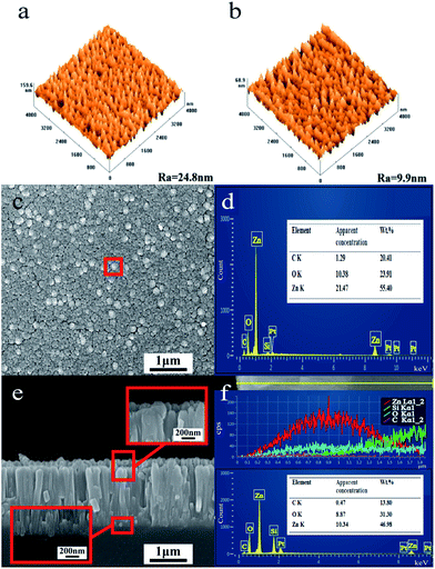
The surface and cross-sectional morphologies of the GZN composite film were investigated via atomic force microscopy (AFM, Veeco Instrument NanoScope D3100, USA) and scanning electron microscopy with an energy dispersive spectrometer (SEM, Carl Zeiss Auria-39-35, Germany), respectively. For AFM measurements, the scanning area was fixed at 4 × 4 μm2 and measurements were in the near central region of the sample, via tapping mode. The surface topology derived from the AFM measurements represents the surface roughness of the GZN composite film. The crystal structure of the GZN composite film was determined via X-ray diffraction (XRD) using Cu Kα radiation (XRD, Bruker D8). Raman spectra were collected using a Renishaw inVia Raman microscope, with excitation at room temperature using an excitation laser wavelength of 514 nm. The chemical states of the elements in graphene were analyzed using an X-ray photoelectron spectrometer (XPS, Thermo Fisher Scientific, K-Alpha), which was equipped with a monochromatic Mg Kα X-ray source (hν = 1253.6 eV), with the anode operating at 14.0 kV and current emission of 18 mA. Data analysis was carried out using XPS Peak4.1 (the Chinese University of Hong Kong, China) with a variation of Gaussian (90–80%) ± Lorentzian (10–20%) profiles.In order to understand the optical properties of GZN composite film, an ultraviolet (UV)-visible spectrophotometer (TU-1901, China) was employed to record the total transmittance and absorption spectra from 250 to 800 nm.
Water contact angle investigations were performed using a contact angle system (XG-CAMC1, Shanghai Xuanyichuangxi Industrial Equipment Co., Ltd. China). Distilled water was used as the testing liquid. A 30 W UV lamp was used to irradiate the surfaces of graphene, ZnONRs and GZN composite film. Contact angles were measured using 5 min time intervals and the data were recorded with a 60 s step.
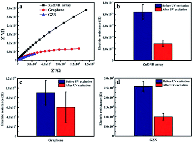
The charge transfer resistance was determined using electrochemical impedance spectra (EIS), which were collected at the open circuit potential in the dark and under UV irradiation with a CHI660E (ChenHua, China). The amplitude of the sinusoidal wave was 5 mV and the frequency range examined was 100 kHz to 0.1 Hz. Electric resistance was measured using a resistance instrument for samples unexposed and exposed to 30 W UV irradiation.
Results and discussion
Morphological and microstructural characterization
AFM images of the surface morphologies of the ZnONR array and GZN composite film are shown in Fig. 2(a) and (b), respectively. The surface roughness of GZN composite film (9.9 nm) is lower than that of the ZnONR array (24.8 nm), as graphene nanosheets with two-dimensional (2D) structure bonded with the ZnONR array. Moreover, the ZnONR array reduced the high aspect ratio of the graphene nanosheets with 2D structure, which causes the formation of a crumpled surface structure in the graphene. The crumpled graphene could induce an areal-density increase to obtain higher optical absorption per unit area. As reported in the literature,30–35 graphene, as an acceptor and bridge for the ZnO semiconductor, can facilitate electron transfer and slow down the recombination of charge carriers; therefore, interactions between graphene and ZnO can greatly improve the photoresponsivity. Fig. 2(c) shows a top-view SEM image of GZN composite film prepared via DGPSA methods. The results indicate that ZnONRs with a rod diameter of around 140 nm grow on the surface of the quartz substrate. Simultaneously, it can been seen from the top-view image that the GZN composite film is compact and uniform due to the high sputtering yield provided by the double-glow plasma discharge. In Fig. 2(d), an area-scanning energy spectrum of the GZN film reveals the occurrence of carbon, zinc and oxygen peaks, which implies the existence of graphene and ZnO in the GZN film. A typical cross-sectional SEM image of GZN composite film is shown in Fig. 2(e). Well-aligned ZnONRs, with a length of 1.5 μm, are observed and the high-magnification images of the interface exhibit the good adhesion between the GZN film and the quartz substrate. The ZnONRs can shorten the path of charge transfer and enhance the scattering of photons effectively. The cross-sectional element distribution in the GZN film is analyzed using the line-scanning energy spectrum in Fig. 2(f). The distribution of carbon, zinc and oxygen elements shows similar trends to the substrate along the surface, from which the existence of graphene bonded into ZnONR arrays can be deduced.The XRD pattern of GZN composite film is shown in Fig. 3(a). A sharp diffraction peak from crystalline ZnO, which is preferably grown along the (002) direction, at 2θ = 34.98° can be observed and the half width is only 0.236°, due to the high crystallinity of ZnO. This indicates that the ZnONRs are well-oriented in the direction of the c-axis, which is perpendicular to the substrate surface. Such an orientation of ZnO is an acceptable point, since the (002) plane of ZnO has the lowest surface energy.36,37 The enlarged image between 10 and 30° shows a broad diffraction peak at 22.50°; this is interrelated with short-range order in the stacked graphene nanosheets.38
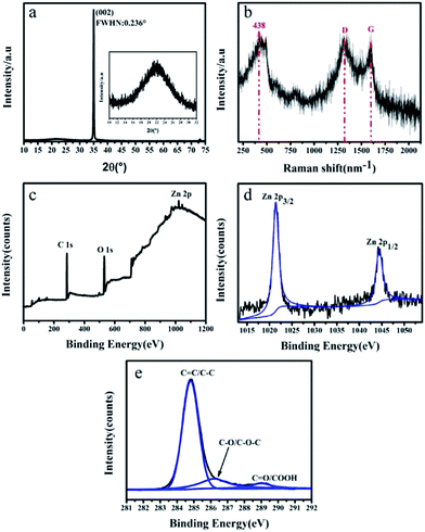 | ||
| Fig. 3 (a) XRD pattern of GZN, (b) Raman spectra of GZN, (c) XPS survey scan of GZN, (d) Zn 2p XPS spectra, and (e) XPS spectra of C 1s. | ||
Raman spectroscopy is employed to identify the crystallographic structures of GZN composite film, especially to distinguish ordered and disordered carbon related structures, as shown in Fig. 3(b). The peak at 438 cm−1 is due to the E2 vibrational mode, which is characteristic of wurtzite phase ZnO.39 Simultaneously, the peaks at 1350 cm−1 and 1590 cm−1 correspond to the D and G bands of graphene. The G peak results from the presence of sp2 carbon, whereas the D peak results from the presence of disorder in the graphene nanosheet structure.40
XPS was performed to confirm the presence of graphene in the GZN composite film. The XPS survey scan of GZN in Fig. 3(c) confirms the existence of carbon, oxygen and zinc elements, without other impurity elements. Fig. 3(d) presents the original and fitted Zn 2p XPS spectra, obtained from the GZN composite film. There are two typical strong peaks at 1021.5 eV and 1044.5 eV, corresponding to the doublet of Zn 2p3/2 and Zn 2p1/2, respectively, which can be attributed to the existence of Zn–O bonds. In Fig. 3(e), we present C 1s spectra of GZN composite film. The spectra are deconvoluted into three lines corresponding to C![[double bond, length as m-dash]](https://www.rsc.org/images/entities/char_e001.gif) C/C–C bonds centered at a binding energy of 284.8 eV, oxygen-containing functional groups (C–O/C–O–C) situated at 286.2 eV, and C
C/C–C bonds centered at a binding energy of 284.8 eV, oxygen-containing functional groups (C–O/C–O–C) situated at 286.2 eV, and C![[double bond, length as m-dash]](https://www.rsc.org/images/entities/char_e001.gif) O/COOH groups at 288.9 eV.41 Among these, the C
O/COOH groups at 288.9 eV.41 Among these, the C![[double bond, length as m-dash]](https://www.rsc.org/images/entities/char_e001.gif) C/C–C bonds correspond to the graphite-like (sp2) structure of the conjugated honeycomb lattice. Graphene is deposited onto the ZnONRs via electrostatic interaction energy, which can improve charge transfer at the interface.42 The binding energies and relative area percentages for GZN composite film are shown in Table 3. The XPS data results indicate that the intensity of the peaks corresponding to the oxygen functional groups confirms the presence of partial graphene oxide in the composite film.
C/C–C bonds correspond to the graphite-like (sp2) structure of the conjugated honeycomb lattice. Graphene is deposited onto the ZnONRs via electrostatic interaction energy, which can improve charge transfer at the interface.42 The binding energies and relative area percentages for GZN composite film are shown in Table 3. The XPS data results indicate that the intensity of the peaks corresponding to the oxygen functional groups confirms the presence of partial graphene oxide in the composite film.
C![[double bond, length as m-dash]](https://www.rsc.org/images/entities/char_e001.gif) C/C–C C/C–C |
C–O/C–O–C | C![[double bond, length as m-dash]](https://www.rsc.org/images/entities/char_e001.gif) O/COOH O/COOH |
|
|---|---|---|---|
| Peak/eV | 284.6 | 286.2 | 288.9 |
| Content/% | 75.05 | 17.82 | 7.11 |
Effects of the introduction of graphene on the photoelectrochemical properties of GZN composite film
To investigate the optical response properties of GZN composite film, UV-visible spectroscopy was employed. As can be seen from Fig. 4(a), the average optical transmittance of the ZnONR array with 1.5 μm thickness is nearly 95% in the visible-light region before the deposition of graphene nanosheets. After the deposition of graphene nanosheets, the total transmittance was maintained at nearly 75%, which confirms the average number of graphene nanosheets to be more than five.43 Compared with the ZnONR array, the decrease in transmittance in the visible-light region for the GZN composite film is mainly a result of reflection and absorption at the interface between the graphene nanosheets and ZnONRs. It can be seen from Fig. 5(b) that the absorption edge of the ZnONRs is at about 375 nm; no apparent absorption is observed in the visible-light region. After the introduction of graphene, the absorption edge of the GZN composite film undergoes a red shift, and the absorption intensity increases significantly at wavelengths greater than 375 nm, which might be attributed to the enhancement in the charge transport properties of the GZN composite film.44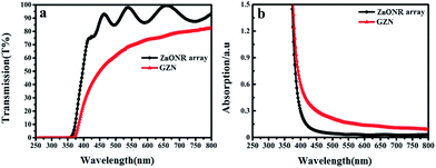 | ||
| Fig. 4 (a) The UV-visible transmission of the ZnONR array and GZN. (b) The UV-visible absorbance of the ZnONR array and GZN. | ||
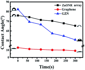 | ||
| Fig. 5 The relationship between contact angle and ultraviolet irradiation time for the ZnONR array, graphene film and GZN. | ||
UV-induced contact angles were used to analyze the effects of the optical response on the surface hydrophilic–hydrophobic properties of GZN composite film. The relationships between the change in contact angle and the UV irradiation time for the ZnONR array, graphene film and GZN composite film are shown in Fig. 5. It can be seen that the contact angles for all three films decrease upon prolonged UV irradiation. The obvious reduction in contact angle for GZN composite film occurs from 82.4° to 51°, at a rate of 6.6° min−1, as compared with that for the ZnONR array (2° min−1) and graphene film (0.86° min−1). Under the conditions of being exposed to UV irradiation, ZnO generates pairs of electrons and holes, and the photogenerated electrons react with oxygen (O2) to produce superoxide radical anions (O2−). Subsequently, the photogenerated holes react with water to produce hydroxyl (OH) radicals. In the process, oxygen atoms are ejected, creating oxygen vacancies.45 The decrease in the contact angle under UV irradiation was attributed to the dissociative adsorption of water molecules on the photogenerated surface defect oxygen vacancy sites.42 In the case of GZN composite film, after quickly moving through the graphene/ZnO interface, the photogenerated electrons transfer to the crumpled graphene surface and result in photochemical reactions. The rapid production of oxygen vacancies leads to the contact angle decreasing at a rapid rate. In other words, the introduction of crumpled graphene to GZN composite film could provide an effective transmission channel for photogenerated electrons and weaken the recombination of charge carriers.
As has been reported, graphene is an excellent electron acceptor and transporter due to its 2D conjugation structure.46 Graphene/ZnO interfacial charge transfer is a vital factor for its photoelectrical activity, which can be investigated via typical electrochemical impedance spectra (EIS). EIS of the ZnONR array, graphene film and GZN composite film in as-prepared photoanodes under ultraviolet irradiation are shown in Fig. 6(a). Semicircles in the curves in the EIS spectra reflect interfacial impedance occurring at the surface of the electrode, and smaller semicircle curves reveal lower electrochemical impedance, which can help charge transfer easily.26,47 It is observed that the arc radius for the GZN composite film is much smaller than that for the ZnONR array and slightly smaller than that for the graphene film, indicating that the synergistic effects of these two component units can reduce impedance in the solid state interfacial layer and enhance charge transfer at the surface. Fortunately, the presence of graphene nanosheets can be beneficial for the transport of photo-induced electrons, as a result of the excellent conductivity of graphene, as seen when comparing the plots of electrodes with and without graphene. Fig. 6(b)–(d) show the electric resistance of three films both unexposed and exposed to UV irradiation. It can be noted that the electric resistance of the ZnONR array and graphene film remains in the range of GΩ, while that of GZN composite film greatly decreases to the range of kΩ. The decrease in the electric resistance of GZN composite film depends on the formation of electrical interactions and interelectron transfer at the interface between the graphene nanosheets and ZnONR array. Furthermore, the electric resistances of all three types of film are reduced after ultraviolet irradiation, due to the fact that electron–hole pairs were generated and the density of charge carriers increased under UV excitation.48
Conclusions
In summary, a novel method was developed to prepare large-area graphene/ZnO nanorod (GZN) composite film using a simple two-step DGPSA process. The GZN composite film exhibited obvious UV photoresponsive behavior; in particular, the introduction of graphene to ZnO nanorod film has an obvious influence on the photoelectrochemical properties of GZN composite film. The photoelectrochemical properties of GZN composite film under UV irradiation indicated that the graphene/ZnO interface can provide an effective transmission channel for photogenerated electrons and weaken the recombination of charge carriers. The synergistic effects of the ZnONR array and graphene nanosheets can reduce the interfacial impedance and enhance charge transfer. Therefore, GZN as a photoanode material could have potential applications in UV photoelectrochemical detection or solar cells. Furthermore, this work can be considered as a competitive candidate for providing methods for the large-area fabrication of graphene film and GZN composite films.Conflicts of interest
There are no conflicts to declare.Acknowledgements
This project is supported by the Natural Science Foundation-Outstanding Youth Foundation of the Jiangsu Province of China (No. BK20160091), the National Natural Science Foundation of China (No. 51405242), the Six Talent Peaks Project of Jiangsu Province, China (No. GDZB-046) and the Open Project of the Jiangsu Key Laboratory of Advanced Micro/Nano Materials and Technology (No. 30917014106).References
- J. Y. Kim, H. Jeong and D. J. Jang, J. Nanopart. Res., 2011, 13(12), 6699–6706 CrossRef CAS.
- S. M. Peng, Y. K. Su and L. W. Ji, et al., Electrochem. Solid-State Lett., 2011, 14(3), J13 CrossRef CAS.
- D. Cammi, R. Röder and C. Ronning, J. Phys. D: Appl. Phys., 2014, 47(39), 394014 CrossRef.
- M. Tanveer, A. Habib and M. B. Khan, Mater. Sci. Eng., B, 2012, 177(13), 1144–1148 CrossRef CAS.
- H. D. Cho, A. S. Zakirov and S. U. Yuldashev, et al., Nanotechnology, 2012, 23(11), 115401 CrossRef PubMed.
- N. K. Ibrayev, B. R. Ilyassov and D. A. Afanasyev, Opt. Spectrosc., 2017, 122(3), 462–468 CrossRef CAS.
- K. S. Novoselov, A. K. Geim and S. V. Morozov, et al., Nature, 2005, 438(7065), 197–200 CrossRef CAS PubMed.
- A. C. Ferrari, Nat. Photonics, 2016, 4(9), 611–622 Search PubMed.
- K. I. Bolotin, K. J. Sikes and Z. Jiang, et al., Solid State Commun., 2008, 146(9–10), 351–355 CrossRef CAS.
- G. Cravotto and P. Cintas, Chemistry, 2010, 16(18), 5246 CrossRef CAS PubMed.
- K. S. Kim, Y. Zhao and H. Jang, et al., Nature, 2009, 457(7230), 706 CrossRef CAS PubMed.
- G. Eda, G. Fanchini and M. Chhowalla, Nat. Nanotechnol., 2008, 3(5), 270 CrossRef CAS PubMed.
- A. A. Balandin, S. Ghosh and W. Bao, et al., Nano Lett., 2008, 8(3), 902 CrossRef CAS PubMed.
- X. Wang, L. Zhi and K. Müllen, Nano Lett., 2008, 8(1), 323 CrossRef CAS PubMed.
- H. Park, S. Chang and J. Jean, et al., Nano Lett., 2013, 13(1), 233 CrossRef CAS PubMed.
- M. Dutta, S. Sarkar and T. Ghosh, et al., J. Phys. Chem. C, 2015, 116(38), 20127–20131 Search PubMed.
- J. Wu, X. Shen and J. Lei, et al., Appl. Surf. Sci., 2010, 256(9), 2826–2830 CrossRef CAS.
- R. Zou, G. He and K. Xu, et al., J. Mater. Chem. A, 2013, 1(29), 8445–8452 CAS.
- P. Wang, D. Wang and M. Zhang, et al., Sens. Actuators, B, 2016, 230, 477–484 CrossRef CAS.
- Z. Bai, X. Yan and Z. Kang, et al., Nano Energy, 2015, 14, 392–400 CrossRef CAS.
- Y. Zhang, H. Li and L. Pan, et al., J. Electroanal. Chem., 2009, 634(1), 68–71 CrossRef CAS.
- T. Lu, L. Pan and H. Li, et al., J. Alloys Compd., 2011, 509(18), 5488–5492 CrossRef CAS.
- R. C. Pawar and C. S. Lee, Appl. Catal., B, 2014, 144(1), 57–65 CrossRef CAS.
- W. C. Chang, T. C. Tseng and W. C. Yu, et al., J Nanosci. Nanotechnol., 2016, 16(9), 9160–9165 CrossRef CAS.
- Z. Wang, X. Zhan and Y. Wang, et al., Nanoscale, 2012, 4(8), 2678 RSC.
- Z. Kang, Y. Gu and X. Yan, et al., Biosens. Bioelectron., 2015, 64(64C), 499–504 CrossRef CAS PubMed.
- K. Chung, C. H. Lee and G. C. Yi, Science, 2010, 330(6004), 655 CrossRef CAS PubMed.
- S. Ameen, M. S. Akhtar and M. Song, et al., ACS Appl. Mater. Interfaces, 2012, 4(8), 4405 CAS.
- B. Nie, J. G. Hu and L. B. Luo, et al., Small, 2013, 9(17), 2872 CrossRef CAS PubMed.
- O. Akhavan, ACS Nano, 2010, 4(7), 4174 CrossRef CAS PubMed.
- J. Song, H. B. Yang and X. Wang, et al., ACS Appl. Mater. Interfaces, 2012, 4(7), 3712–3717 CAS.
- J. L. Song, X. Wang and C. C. Wong, Electrochim. Acta, 2015, 173, 834–838 CrossRef CAS.
- Y. Liu, Z. Chen and Z. Kang, et al., J. Phys. Chem. C, 2008, 112(25), 9214–9218 CAS.
- H. Wang, J. T. Robinson and X. Li, et al., J. Am. Chem. Soc., 2009, 131(29), 9910–9911 CrossRef CAS PubMed.
- P. Kang, M. C. Wang and P. M. Knapp, et al., Adv. Mater., 2016, 28(23), 4639–4645 CrossRef CAS PubMed.
- Y. Caglar, S. Ilican and M. Caglar, et al., Spectrochim. Acta, Part A, 2007, 67(3), 1113–1119 CrossRef PubMed.
- S. S. Lin and J. L. Huang, Surf. Coat. Technol., 2003, 185(2), 222–227 Search PubMed.
- C. Nethravathi and M. Rajamathi, Carbon, 2008, 46(14), 1994–1998 CrossRef CAS.
- R. Shabannia, Prog. Nat. Sci.: Mater. Int., 2015, 25(2), 95–100 CrossRef CAS.
- A. C. Ferrari, Solid State Commun., 2007, 143(1–2), 47–57 CrossRef CAS.
- Y. Matsumoto, M. Koinuma and S. Ida, et al., J. Phys. Chem. C, 2011, 115(39), 19280–19286 CAS.
- J. E. Lee, N. T. Khoa and S. W. Kim, et al., Mater. Chem. Phys., 2015, 164, 29–35 CrossRef CAS.
- R. R. Nair, P. Blake and A. N. Grigorenko, et al., Science, 2008, 320(5881), 1308 CrossRef CAS PubMed.
- T. Xu, L. Zhang and H. Cheng, et al., Appl. Catal., B, 2011, 101(3–4), 382–387 CrossRef CAS.
- A. Fujishima, T. N. Rao and D. A. Tryk, J. Photochem. Photobiol., C, 2000, 1(1), 1–21 CrossRef CAS.
- M. Freitag, Nat. Nanotechnol., 2008, 3(8), 455–457 CrossRef CAS PubMed.
- D. Wang, D. Choi and J. Li, et al., ACS Nano, 2009, 3(4), 907 CrossRef CAS PubMed.
- K. Li, M. Gao and Z. Huang, et al., J. Mater. Sci.: Mater. Electron., 2017, 1–5 Search PubMed.
| This journal is © The Royal Society of Chemistry 2017 |

