DOI:
10.1039/C7RA10873G
(Paper)
RSC Adv., 2017,
7, 53503-53508
Fabrication of sub-1 nm gap electrodes using metal-mask patterning and conductivity measurements of molecules in nanoscale spaces†
Received
2nd October 2017
, Accepted 15th November 2017
First published on 21st November 2017
Abstract
We developed a procedure for fabricating sub-1 nm gap Au electrodes using a metal mask for electrode patterning. Self-aligned nanogap formation was achieved using an electromigration method during metal deposition. We also measured the electric conductivities of organic molecules using the new nanogap electrodes. Because the new procedure does not involve wet processing, the ranges of possible electrode and substrate materials for the nanogap electrodes are greatly expanded. Finally, we discussed the molecular orbital energies of bridging and nonbridging 1,4-benzenedithiol molecules between Au electrodes. The new procedure for the fabrication of nanogap electrodes is expected to be useful for measuring the electrical properties of various nanoscale materials.
1. Introduction
Nanogap electrodes comprise two electrodes facing one another across a nanometer-scale gap. They can be used to investigate the electrical properties of molecules and nanosized materials such as organic molecules and nanoparticles.1–3 Because nanogap electrodes exhibit various characteristic phenomena, such as surface plasmon enhancement, nonvolatile resistance change, and field emission,4–6 nanogap electrodes have great potential in nanophotonic and nanoelectronic applications. The characteristics of nanogap electrodes depend on the metal component of the electrode, the atmosphere, the temperature, the external electric and magnetic fields, and other factors. The width of the nanogap is also a factor that influences the characteristics of nanogap electrodes. Therefore, the fabrication of nanogaps with well-defined widths is critical. Various methods have been applied to form nanogaps with specific widths, like electron-beam lithography,7,8 electroplating,9 molecular lithography,9–12 shadow evaporation,13 and electromigration,14 among others.15–20 In a previous study,21 we successfully developed a method for nanogap fabrication in which a voltage is applied during metal deposition, inducing the electromigration of the metals. We applied this method to form self-aligned nanogaps as small as 1 nm in width and found that the gap width could be controlled by changing the magnitude of the applied voltage. However, most of the methods mentioned above use both dry processing (electron-beam lithography or photolithography) and wet processing (for coating and removing resist layers). Replacing the entire patterning process with only dry processing (e.g., metal-mask patterning) would greatly expand the range of suitable electrode and substrate materials. For example, metal electrodes without adhesion layers or substrates that deform in solvents could be selected as constituents of nanogap electrodes. In general, titanium serves as the adhesion layer between an Au electrode and SiO2 substrate. The titanium layer is more easily oxidized than the Au electrode, and the conductivity of the resulting titanium oxide varies widely.22 The varying resistance of titanium oxides may generate error when measuring the resistance of nanosized materials using nanogap electrodes. Therefore, it is beneficial to conduct measurements using nanogap electrodes without adhesion layers.
The fabrication of nanogap electrodes without wet processing was demonstrated in a previous paper.23 However, because the resulting gap width was over 50 nm, it is difficult to prepare single-molecule-sized nanogaps using the reported method. Furthermore, the accuracy of metal-mask patterning is poor compared with that of photolithography or electron-beam lithography. In this study, we adopted the electromigration method during metal deposition to fabricate nanogaps via metal-mask patterning and confirmed the gap widths using 1,4-benzenedithiol (BDT) which is utilized to fundamental understanding of metal/molecule/metal junctions.24–26 In a previous study,21 we reported that gap size, which was estimated from a tunnelling fitting, was controlled by the magnitude of the bias voltage. To determine the actual gap size, we compared the conduction of molecular wires using the fabricated nanogaps with the various bias voltages.
2. Results and discussion
2.1 Fabrication of nanogap electrodes using metal-mask patterning
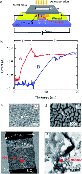
Nanogap electrodes were prepared by two cycles of Au evaporation with metal-mask patterning on a Si substrate covered with a thermally oxidized layer. Fig. 1a shows a schematic diagram of the process during the second evaporation step. During the second deposition step, a voltage was applied across the facing electrodes to induce electromigration. This applied voltage is referred to as the process voltage. Fig. 1b shows the change in current accompanying an increase in Au thickness with (red line or curve A) and without (blue line or curve B) a 0.5 nm thick Cr layer, which acts as an adhesion layer between SiO2 and the Au layer. A process voltage of 10 V was applied during processes A and B. Curve A shows a similar change in current compared to that reported in a previous study.21 In the early stages of deposition, where the deposition thickness in process A was under ∼5 nm (stage I), a rapid increase in current was observed; this increase was attributed to changes in the tunnelling current. The 5 nm threshold observed in this study is larger than the 3 nm threshold reported in previous studies.21 This difference in deposition thickness was likely influenced by the size of the prestructure gap (30 μm in this study and 4 μm in the previous one). Following the large current reduction at the end of stage I, the current remained fairly constant at 42 μA. This indicates that a nanogap structure was formed during stage II and that nanogap fabrication was achieved by metal-mask patterning. As shown in curve B in Fig. 1b, stage I continued until the thickness of the metal layer reached approximately 12 nm. Fig. 1c and d show field-emission scanning electron microscopy (FE-SEM) images of the metal islands on the substrates with and without a Cr layer, respectively, when the current reached 100 nA. The sizes of the metal islands in Fig. 1d are clearly larger than in Fig. 1c. An adhesion layer was not deposited in process B, suggesting that the Au atoms actively migrated, and a large volume of Au atoms was necessary to form immobile islands on the substrate. Therefore, the thickness at the end of stage I was influenced by the strength of adhesion between the substrate and the evaporated materials. The current in process B became saturated at 97 μA, suggesting that a nanogap structure was formed. Fig. 1e presents an FE-SEM image of a sample fabricated without a Cr layer, while Fig. 1f shows a magnified image of the area indicated by the red arrow in Fig. 1e. The formed nanogap structure appears as an uninterrupted valley across the entire 30 μm wide second Au layer. Wide gaps are partly shown around the blue arrow in Fig. 1e. However, thin gold films and nanogaps were also formed inside the wide gaps. This suggested that the crater-like, wide gaps were formed at the end of stage I around 12 nm in Fig. 2b, and additional evaporated gold films and new nanogap structures formed after stage I. These results indicate that the nanogap structures self-aligned along the entire width of the 30 μm slit, similar to in previous studies.21,27
 |
| | Fig. 1 (a) Schematic of the fabrication procedure during the second evaporation under an applied voltage. (b) Dependence of current on Au layer thickness for electrodes with (A) and without (B) a Cr layer on the substrate. FE-SEM images of the evaporated film at 100 nA in curve A (c) and curve B (d). (e) FE-SEM image of the fabricated nanogap electrode without a Cr layer and a process voltage of 10 V. The nanogap is indicated by the red translucent bands. (f) Magnified FE-SEM image of the area indicated by the red arrow in (e). | |
 |
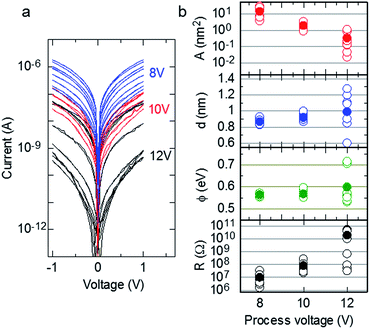
| | Fig. 2 (a) Experimental I–V curves (n = 8) for samples fabricated without Cr layers at process voltages of 8, 10, and 12 V. (b) Dependences of tunnelling emission area (A), gap size (d), barrier height (ϕ), and the measured resistance at 0.1 V (R) on the process voltage. A, d, and ϕ were estimated from fitting the I–V curves using eqn (1). | |
2.2 Estimation of fabricated gap size
The I–V curves of the fabricated samples without Cr layers are shown in Fig. 2a. Process voltages of 8, 10, and 12 V were applied during sample fabrication, and the I–V curves of eight samples were measured at each process voltage. The average resistances of the samples prepared with process voltages of 8, 10, and 12 V were 9.61 ± 10.6 MΩ, 79.7 ± 77.4 MΩ, and 17.9 ± 22.2 GΩ, respectively. The resistance of individual samples varied at each process voltage, but the average resistance increased with increasing process voltage. Assuming a simple tunnelling effect, we extracted the structural parameters of the fabricated nanogaps from their observed I–V characteristics based on the tunnelling equation:| |
 | (1) |
where I(V) is tunnelling current; e = 1.60 × 10⁻¹⁹; h = 6.62 × 10⁻³⁴; m = 9.11 × 10⁻³¹; and V, d, A, and ϕ denote the applied voltage, the gap width, the tunnelling emission area, and the barrier height, respectively.28–30 Fig. 2b plots the dependences of A (top panel), d (upper middle panel), ϕ (lower middle panel), and resistance (bottom panel) on process voltage. The resistance was measured at 0.1 V, and d, A, and ϕ were estimated by fitting eqn (1). The open and closed circles in Fig. 2b indicate individual and averaged data points, respectively. Details of fitting data is shown in the ESI.† The data for the process voltage of 12 V fluctuate considerably; however, the average gap size generally increased with increasing process voltage.
This result is similar to the behaviour reported in the previous report21 and suggests that the resistance of the fabricated nanogap can be controlled by changing the magnitude of the process voltage, as observed for the resistance switching of nanogap electrodes.6
2.3 Conductivity measurements of BDT in nanogap electrodes
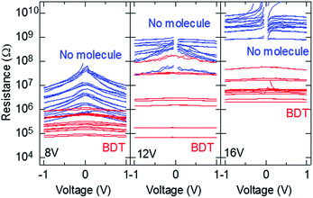
To confirm that the gap width of the fabricated nanogap electrode was approximately 1 nm, we employed a bridging structure composed of BDT, which has a molecular length of approximately 0.9 nm. For the samples fabricated at a process voltage of 8 V, the gap sizes were almost lower than 0.9 nm (Fig. 2b). Fig. 3 presents the resistance–voltage (R–V) curves of the nanogap electrodes before and after immersion in BDT solution. Table 1 lists the resistances at 0.1 V before and after immersion in BDT and rates, resistance of which is below single bridged BDT between Au electrodes (∼1/0.011 G0, where G0 is quantum conductance).31–33
 |
| | Fig. 3 Experimental R–V curves (n = 16, 8, and 12 at process voltages of 8, 12, and 16 V, respectively) of nanogap electrodes before and after immersion in BDT solution. | |
Table 1 Resistance measured at 0.1 V before (no molecule) and after (+BDT) immersion in 1 mM BDT ethanol solution. Rate of resistance of “+BDT” below the single Au–BDT–Au junction. Each resistance value is the average of all observed samples. Reported errors are the standard deviations of all observed samples
| Vprocess |
8 V |
12 V |
16 V |
| No molecule |
13.6 ± 14.9 MΩ |
417 ± 234 MΩ |
3.83 ± 2.79 GΩ |
| +BDT |
432 ± 328 kΩ |
27.4 ± 50.4 MΩ |
7.80 ± 6.13 MΩ |
| <1/0.011 G0 |
100% (16/16) |
25% (2/8) |
0% (0/12) |
The samples were fabricated without a Cr layer at process voltages of 8, 12, and 16 V. The observed currents of no molecule at 16 V were considerably small and close to the sensitivity limit of our source meter. The R–V curves contain the contribution leakage currents of thin metal layers around the sides of metal electrode parts that are formed by wraps of evaporated Au atoms during the second Au deposition using metal-mask patterning. Therefore, fitting using eqn (1) was difficult, and gap size could not be estimated. However, among the three process voltages, 16 V resulted in the largest resistances, suggesting that the gap sizes produced at 16 V were also rather large. The nonlinearity in the I–V curves was clearly suppressed after immersion in BDT solutions. The average resistances of the electrodes (n = 16) formed at the process voltage of 8 V were 13.6 ± 14.9 MΩ and 432 ± 328 kΩ before and after immersion, respectively. Some of the sample resistances were lower after immersion in BDT than before immersion; however, when each sample is compared, large reductions in resistance were observed and the magnitude of the resistance was below that of a single bridged BDT in all electrodes. This suggests that BDT successfully bridged the gaps in almost all the electrodes; thus, the widths of the gaps in the fabricated electrodes were close to or below 0.9 nm. On the other hand, large reductions in resistance were observed in all samples formed at the process voltages of 12 and 16 V. The rates at 12 and 16 V, resistance of which is below single bridged BDT, were lower, and the process voltages were higher. Because the rate at 16 V is 0%, note that it is clearly evident that any BDT bridging with high conduction, the magnitude of which is 0.011 G0, is not formed in any samples at a process voltage of 16 V. This suggests that the nanogap size could be controlled by varying the magnitude of the process voltage, as mentioned earlier. However, in previous studies using mechanically controlled break-junction (MCBJ) techniques, the conductivity of BDT bridged between Au electrodes varied in magnitude with the bridging conditions.34
2.4 Evaluation of BDT bridging using single-level tunnelling transport model
To evaluate the bridging conditions, we investigated the I–V curves of the nanogap electrodes after immersion in BDT. The I–V characteristics were evaluated using the single-level tunnelling transport model,34,35 in which the observed current I(V) is given by| |
 | (2) |
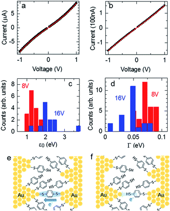
where N is the number of BDT molecules, ε0 is the energy of the molecular orbital involved in the charge-transfer process, and ΓL and ΓR are the coupling strengths between the molecular wire and the left and right Au electrodes, respectively. Because we used fixed nanogap electrodes in this study, we were not able to determine the number of bridging BDT molecules, as in MCBJ studies. Therefore, we defined the number of BDT molecules as N, and the integral N was calculated by dividing the observed conductance by the conductance of a single BDT molecule. When N was below 1, N was defined as 1. The validity of this strategy is discussed further in the ESI.† Fig. 4a and b show the typical experimental and fitted I–V curves of BDT conductance obtained using the fabricated nanogap electrodes with process voltages of 8 and 16 V, respectively. As mentioned above, the curves likely contain contributions from BDT bridging with high conductance (G = 0.011 G0) at 8 V and rarely contain the contribution at 16 V. Fig. 4c and d show the distributions of ε0 and Γ obtained from fitting the I–V curves to eqn (2). The peaks of ε0 and Γ were clearly different for the process voltages of 8 and 16 V. Table 2 lists the average values of estimated ε0 and Γ. At the process voltage of 8 V, the average ε0 was 1.20 eV, in close agreement with the molecular orbital energy (EF − EHOMO) reported in a previous experimental study.36 On the other hand, the average ε0 at the process voltage of 16 V was 2.06 eV, which agrees closely with the value reported in previous experimental studies of benzene-thiol on Au surfaces.37,38 These results suggest that the difference in ε0 between the two process voltages was caused by the difference in charge transfer between the BDT molecule and both sides or single sides of the Au electrodes. This indicates that bridging and nonbridging structures were formed at process voltages of 8 and 16 V, as in Fig. 4e and f, respectively. These results indicate that the bridged structure can be controlled by employing prefabricated nanogap electrodes formed at various process voltages.
 |
| | Fig. 4 I–V curves of nanogap electrodes formed at process voltages of 8 V (a) and 16 V (b) after immersion in BDT solution. Closed black circles indicate the measured curves, and the red lines are the fits with eqn (2) using N = 8, ΓL = 0.0641 eV, ΓR = 0.0653 eV, and ε0 = 1.19 eV for (a) and N = 1, ΓL = 0.0448 eV, ΓR = 0.0442 eV, and ε0 = 2.06 eV for (b). Dependences of ε0 (c) and Γ (d) on process voltage. Schematic models of bridging (e) and nonbridging (f) Au–BDT–Au junctions in the nanogap electrodes. | |
Table 2 Averages and standard deviations of coupling strength between the molecular wire and both Au electrodes (left (ΓL) and right (ΓR)) and energy of the molecular orbital (ε0). Individual ΓL, ΓR, and ε0 were estimated using the single-level tunnelling transport model
| Vprocess |
8 V (16 samples) |
16 V (12 samples) |
| ΓL (eV) |
0.0652 ± 0.0120 |
0.0511 ± 0.0349 |
| ΓR (eV) |
0.0657 ± 0.0113 |
0.0514 ± 0.0347 |
| ε0 (eV) |
1.20 ± 0.198 |
2.06 ± 0.599 |
3. Methods
3.1 Electrodes preparation
Nanogap electrodes were prepared by two cycles of Au evaporation with metal-mask patterning on a Si substrate covered with a 300 nm thick thermally oxidized layer. Fig. 1a shows a schematic diagram of the process during the second evaporation step. First, prestructures comprising 50 nm thick Au electrodes with a 30 μm gap were fabricated (first metal) using metal-mask patterning. Another metal mask with a slit structure (width = 30 μm) was then laid across the 30 μm gap of the prestructure during the second cycle of metal evaporation. The deposition was carried out using a thermal evaporator. The deposition rate, film thickness, and substrate temperature were typically 0.02 nm s−1, 20 nm, and room temperature, respectively. During the second deposition step, a process voltage was applied across the facing electrodes to induce electromigration and the current was measured using a Keithley 2612 SourceMeter. To prevent conduction between the electrodes and the metal mask, a 100 nm thick SiO2 layer was deposited on the back of the metal mask by sputter deposition. The fabricated nanogaps were evaluated using FE-SEM. The electronic properties of the nanogap electrodes were measured using the SourceMeter at room temperature under vacuum.
3.2 BDT bridging preparation and conductivity measurements
To determine the nanogap size, the conductivity of 1,4-benzenedithiol (BDT), which has a molecular length of approximately 0.9 nm, was measured using the fabricated nanogap electrodes. The Au nanogap electrodes were immersed in a 1 mM BDT ethanol solution at room temperature for one day. After being removed from solution, the current–voltage (I–V) characteristics of the electrodes were measured using the SourceMeter at room temperature in a vacuum probe station.
4. Conclusions
We successfully fabricated sub-1 nm nanogap electrodes using metal-mask patterning and demonstrated that nanogap electrodes can be fabricated without any adhesion layer between the electrodes and substrate. In other words, nanogap electrodes can be fabricated using only dry processing, thereby expanding the range of suitable electrode and substrate materials compared to conventional methods. Furthermore, we measured the conductivities of organic molecules using the fabricated nanogap electrodes, demonstrating that our new fabrication method can facilitate the electrical characterization of various molecules in nanoscale spaces.
Conflicts of interest
There are no conflicts to declare.
Acknowledgements
The authors acknowledge financial support from the Japan Society for the Promotion of Science (JSPS) through a Grant-in-Aid for Scientific Research (no. JP16H00974, JP17H05146, JP15H05757, and JP26110508). The authors extend their deep appreciation to Dr Takeshi Kobayashi and Dr Touru Sumiya of the National Institute of Advanced Industrial Science and Technology (AIST) for advice on a wide range of issues related to this study. The fabrication of the materials in this study was partly supported by the AIST Nano-Processing Facility.
References
- A. Bezryadin, C. Dekker and G. Schmid, Appl. Phys. Lett., 1997, 71, 1273 CrossRef CAS.
- H. Song, M. A. Reed and T. Lee, Adv. Mater., 2011, 23, 1583 CrossRef CAS PubMed.
- H. Suga, Y. Naitoh, M. Tanaka, M. Horikawa, H. Kobori and T. Shimizu, Appl. Phys. Express, 2009, 2, 055004 CrossRef.
- D. F. P. Pile, T. Ogawa, D. K. Gramotnev, Y. Matsuzaki, K. C. Vernon, K. Yamaguchi, T. Okamoto, M. Haraguchi and M. Fukui, Appl. Phys. Lett., 2005, 87, 261114 CrossRef.
- H. Fujii, S. Kanemaru, H. Hiroshima, S. M. Gorwadkar, T. Matsukawa and J. Itoh, Appl. Surf. Sci., 1999, 146, 203 CrossRef CAS.
- Y. Naitoh, M. Horikawa, H. Abe and T. Shimizu, Nanotechnology, 2006, 17, 5669 CrossRef CAS PubMed.
- M. S. M. Saifullah, T. Ondarçuhu, D. K. Koltsov, C. Joachim and M. E. Welland, Nanotechnology, 2002, 13, 659 CrossRef CAS.
- M. A. Guillorn, D. W. Carr, R. C. Tiberio, E. Greenbaum and M. L. Simpson, J. Vac. Sci. Technol., B: Microelectron. Nanometer Struct.--Process., Meas., Phenom., 2000, 18, 1177 CrossRef CAS.
- A. F. Morpurgo, C. M. Marcus and D. B. Robinson, Appl. Phys. Lett., 1999, 74, 2084 CrossRef CAS.
- H. Tanaka, M. E. Anderson, M. W. Horn and P. S. Weiss, Jpn. J. Appl. Phys., 2004, 43, L950 CrossRef CAS.
- M. E. Anderson, M. Mihok, H. Tanaka, L. P. Tan, M. W. Horn, G. S. McCarty and P. S. Weiss, Adv. Mater., 2006, 18, 1020 CrossRef CAS.
- L. Jiang, H. Dong, Q. Meng, J. Tan, W. Jiang, C. Xu, Z. Wang and W. Hu, Adv. Mater., 2012, 24, 694 CrossRef CAS PubMed.
- Y. Naitoh, K. Tukagoshi, K. Murata and W. Mizutani, e-J. Surf. Sci. Nanotechnol., 2003, 1, 41 CrossRef CAS.
- H. Park, A. K. L. Lim, A. P. Alivisatos, J. Park and P. L. McEuen, Appl. Phys. Lett., 1995, 75, 301 CrossRef.
- P. Gao, Q. Zhang, H. Li and M. B. Chan-Park, Small, 2011, 7, 2195 CrossRef CAS PubMed.
- X. Tian, J. Li and D. Xu, Electrochem. Commun., 2010, 12, 1081 CrossRef CAS.
- Y. Yasutake, K. Kono, M. Kanehara, T. Teranishi, M. R. Buitelaar, C. G. Smith and Y. Majima, Appl. Phys. Lett., 2007, 91, 203107 CrossRef.
- V. M. Serdio, V. T. Muraki, S. Takeshita, D. E. S. Hurtado, S. Kano, T. Teranishi and Y. Majima, RSC Adv., 2015, 5, 22160 RSC.
- T. Li, W. Hu and D. Zhu, Adv. Mater., 2010, 22, 286 CrossRef CAS PubMed.
- L. D. L. S. Valladares, L. L. Felix, A. B. Dominguez, T. Thanos Mitrelias, F. Sfigakis, S. I. Khondaker, C. H. W. Barnes and Y. Majima, Nanotechnology, 2010, 21, 445304 CrossRef PubMed.
- Y. Naitoh, T. Ohata, R. Matsushita, E. Okawa, M. Horikawa, M. Oyama, M. Mukaida, D. F. Wang, M. Kiguchi, K. Tsukagoshi and T. Ishida, ACS Appl. Mater. Interfaces, 2013, 5, 12869 CAS.
- H. Akinaga and H. Shima, Proc. IEEE, 2010, 98, 2237 CrossRef CAS.
- Y. Otsuka, Y. Naitoh, T. Matsumoto, W. Mizutani, H. Tabata and T. Kawai, Nanotechnology, 2004, 15, 1639 CrossRef CAS.
- M. A. Reed, C. Zhou, C. J. Muller, T. P. Burgin and J. M. Tour, Science, 1997, 278, 252 CrossRef CAS.
- M. Tsutsui, M. Taniguchi, K. Shoji, K. Yokota and T. Kawai, Nanoscale, 2009, 1, 164 RSC.
- M. M. Maitani, D. A. A. Ohlberg, Z. Li, D. L. Allara, D. R. Stewart and R. S. Williams, J. Am. Chem. Soc., 2009, 131, 6310 CrossRef CAS PubMed.
- Y. Naitoh, Q. Wei, M. Mukaida and T. Ishida, Appl. Phys. Express, 2016, 9, 035201 CrossRef.
- J. G. Simmons, J. Appl. Phys., 1963, 34, 2581 CrossRef.
- R. Negishi, T. Hasegawa, K. Terabe, M. Aono, T. Ebihara, H. Tanaka and T. Ogawa, Appl. Phys. Lett., 2006, 88, 223111 CrossRef.
- A. Mangin, A. Anthore, M. L. Della Rocca, E. Boulat and P. Lafarge, Phys. Rev. B: Condens. Matter Mater. Phys., 2009, 80, 235432 CrossRef.
- X. Y. Xiao, B. Q. Xu and N. J. Tao, Nano Lett., 2004, 4, 267 CrossRef CAS.
- W. Haiss, C. Wang, R. Jitchati, I. Grace, S. Martín, A. S. Batsanov, S. J. Higgins, M. R. Bryce, C. J. Lambert, P. S. Jensen and R. J. Nichols, J. Phys.: Condens. Matter, 2008, 20, 374119 CrossRef PubMed.
- M. Taniguchi, M. Tsutsui, K. Yokota and T. Kawai, Nanotechnology, 2009, 20, 434008 CrossRef PubMed.
- S. Kaneko, D. Murai, S. Marqués-González, H. Nakamura, Y. Komoto, S. Fujii, T. Nishino, K. Ikeda, K. Tsukagoshi and M. Kiguchi, J. Am. Chem. Soc., 2016, 138, 1294 CrossRef CAS PubMed.
- Y. Komoto, S. Fujii, M. Iwane and M. Kiguchi, J. Mater. Chem. C, 2016, 4, 8842 RSC.
- P. Reddy, S. Y. Jang, R. A. Segalman and A. Majumdar, Science, 2007, 315, 1568 CrossRef CAS PubMed.
- B. S. Kim, J. M. Beebe, Y. Jun, X.-Y. Zhu and C. D. Frisbie, J. Am. Chem. Soc., 2006, 128, 4970 CrossRef CAS PubMed.
- J. M. Beebe, B. S. Kim, J. W. Gadzuk, C. D. Frisbie and J. G. Kushmerick, Phys. Rev. Lett., 2006, 97, 026801 CrossRef PubMed.
Footnote |
| † Electronic supplementary information (ESI) available. See DOI: 10.1039/c7ra10873g |
|
| This journal is © The Royal Society of Chemistry 2017 |
Click here to see how this site uses Cookies. View our privacy policy here.  Open Access Article
 *a,
Ken Albrecht
 bc,
Qingshuo Wei
 d,
Kimihisa Yamamoto
 bc,
Hisashi Shimaa and
Takao Ishidad
