 Open Access Article
Visualizing the bidirectional electron transfer in a Schottky junction consisting of single CdS nanoparticles and a planar gold film†
Zhimin
Li‡
,
Yimin
Fang‡
 ,
Yongjie
Wang
,
Yingyan
Jiang
,
Tao
Liu
and
Wei
Wang
,
Yongjie
Wang
,
Yingyan
Jiang
,
Tao
Liu
and
Wei
Wang
 *
*
State Key Laboratory of Analytical Chemistry for Life Science, School of Chemistry and Chemical Engineering, Nanjing University, Nanjing 210093, China. E-mail: wei.wang@nju.edu.cn
First published on 18th May 2017
Abstract
Bidirectional electron transfer crossing the metal/semiconductor interface regulates the light absorption and carrier separation efficiency of plasmonic-semiconductor hybrid nanomaterials. Existing studies have been largely focused on a localized surface plasmon resonance (LSPR) effect contributed by an ensemble of metal nanomaterials. Herein, we constructed a Schottky junction that consisted of single CdS nanoparticles and a planar gold film, and investigated hot electrons excited by the surface plasmon polaritons (SPPs) propagating in the gold film. When illuminating the interface with blue light, photoinduced electrons were found to inject from the CdS nanoparticle to the gold film. In a reverse process, SPPs were generated on shining a red beam into the gold film via a Kretschmann configuration, resulting in the injection of hot electrons into CdS nanoparticles. A recently developed plasmonic microscopy method was employed to monitor the entire process, providing the ability to image a single nanoparticle to visualize the bidirectional electron transfer dynamics in a Schottky junction involving propagating SPPs. The present study advances the understanding of the mechanism of hot electron transfer, which is anticipated to aid in the rational design and optimization of plasmonic-semiconductor hybrid nanomaterials with broad applications in photocatalysis, photovoltaic devices, and photoelectrochemical sensing.
Introduction
Plasmonic-semiconductor hybrid nanomaterials have been considered as promising solutions to develop highly efficient photocatalysts and photovoltaic devices.1,2 The capability of bi-directional electron transfer crossing the metal/semiconductor interface has resulted in several advantages associated with such hybrid nanomaterials.3 First, plasmonic nanostructures could act as an antenna to improve the solar light absorption efficiency by extending the accessible spectrum to the visible and even near-infrared range. It was difficult for semiconductor materials to directly utilize these low-energy photons due to the large band-gap. Excitation of plasmonic materials generated hot electrons with kinetic energies high enough to overcome the Schottky barrier and to inject into semiconductor nanomaterials for triggering chemical reactions.4 Second, Au or Ag atoms acted as electron reservoirs to enhance the efficiency of carrier separation because a relatively lower Fermi level in the metal facilitated separation and migration of photoinduced electrons.5 In addition, active metal atoms in the plasmonic structures could sometimes act as good catalysts to accelerate chemical reactions occurring on its surface.6Existing studies on hot electron transfers have been mainly focusing on the localized surface plasmon resonance (LSPR) effect that was contributed by the plasmonic (Au or Ag) nanomaterial ensembles.1,4 These approaches faced both materials-based and technical challenges, hampering the comprehensive understanding of the structure–activity relationships. With regards to materials, it is experimentally challenging to synthesize model nanomaterials in which each individual material contains an identical and controllable metal–semiconductor interface. This is because LSPR is known to be highly sensitive to the size, morphology and surface chemistry of metal nanomaterials, which are intrinsically heterogeneous. In contrast to LSPR, propagating surface plasmon polaritons (SPPs), the collective electron oscillations in a planar metal–dielectric interface,7,8 is more suitable when serving as a model system, because such interface can be reliably fabricated with modern technologies. Previous theoretical9,10 and experimental11,12 studies have demonstrated that SPPs sufficiently exhibited high photon-to-hot electron conversion efficiencies11,12 and significantly longer coupling distances up to a few microns.13 However, investigations on the SPPs-induced injection of hot electrons at the single nanoparticle interface are yet to be demonstrated. From a technical perspective, determining the reaction rate of a model reaction (photocatalysis)14 or the potential/current through an interface (photovoltaic)11,15 and measuring the transient absorption spectrum of certain optical probes,16 are two of the major methods to study the efficiency of hot electron transfer. Both techniques provide the averaged behavior of nanomaterial ensembles, which concealed the intrinsic heterogeneity among individuals. Therefore, techniques that can monitor the dynamic process of SPPs-induced charge transfer at single nanoparticle interfaces are highly desired to uncover the underlying mechanism of hot electron transfer.
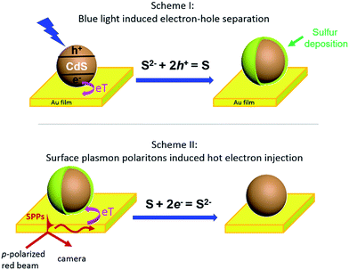
Herein, we present an optical imaging approach that can visualize the bidirectional electron transfer between single CdS nanoparticles and a planar gold film (Fig. 1). On illuminating the interface with blue light, photoinduced electron injection from CdS nanoparticles to the gold film resulted in a hole-rich CdS, which oxidized S2− in the solution to deposit sulfur at the nanoparticle surface (Scheme I). In a reverse process, propagating SPPs were generated in the gold film by a red beam through a Kretschmann configuration, donating energetic hot electrons to the CdS nanoparticle to reduce and dissolve the previously deposited sulfur (Scheme II). The dynamic deposition and dissolution of sulfur on single CdS nanoparticles were visualized in real time by surface plasmon resonance microscopy (SPRM), with an optical contrast reflecting the amount of sulfur.
Results and discussion
SPRM for single CdS NPs imaging
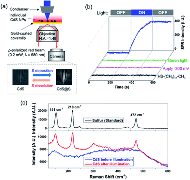
SPRM is an optical microscope that is capable of imaging single nanoparticles based on its disturbance to the SPPs.17–21 A detailed description of the principle, apparatus and image processing of SPRM can be found in our previous studies.20,22–24 Briefly, a red beam (λ = 680 nm) was directed through a microscope objective to illuminate a gold-coated coverslip, resulting in SPPs that were propagating at the gold film–solution interface. The reflected light was captured with a camera to generate a wide-field SPRM image. The presence of a single CdS nanoparticle on the gold film interrupted the SPPs and projected a parabolic pattern in the SPRM image (Fig. S3b†). The cross point in the parabolic pattern represented the location of the nanoparticle and the image contrast, which was referred to as the SPRM intensity, was sensitive to the amount of sulfur because additional sulfur atoms enhanced the disruption of the SPPs.We first demonstrated the capability of the SPRM to monitor the sulfur deposition dynamics during blue light illumination (Scheme I). Spherical CdS nanoparticles with a typical diameter of 160 nm were synthesized and characterized following a previous report (Fig. S1†).25 Individual CdS nanoparticles were deposited onto the gold-coated coverslip with the addition of a suspension of CdS nanoparticles. In order to distinguish an individual nanoparticle, a very low deposition density was selected (∼10 nanoparticles in a field of 60 × 80 μm2) by adjusting the concentration and the incubation time. In the presence of 0.05 mM Na2S, the SPRM intensity was found to gradually increase after the illumination of blue light at the 200th s, as shown in Fig. 2b (blue curve). The SPRM intensity remained unchanged after the withdrawal of blue light at the 400th s, suggesting a stable change in the CdS nanoparticles.
Bidirectional electron transfer at the Schottky junction
Several control experiments were performed to demonstrate that photoinduced electron transfer was responsible for the increased SPRM intensity. On utilizing a green light for illumination (540–560 nm) with a similar power density, no SPRM change was observed (green curve). This is consistent with the absorption spectrum of the as-prepared CdS nanoparticles, which exhibited an absorption edge at 540 nm (Fig. S2†). Furthermore, no increase in the SPRM intensity was observed by blocking the possible electron transfer between the CdS nanoparticles and gold film with a negative potential (−300 mV, magenta curve) or an insulating HS–(CH2)17–CH3 layer (black curve).It was found that the photoinduced electron transfer from the CdS nanoparticle to gold film resulted in hole-rich CdS nanoparticles, which oxidized S2− to deposit sulfur atoms at the surface of CdS. The presence of sulfur deposition was evidenced by comparing the Raman spectra of CdS nanoparticles before and after illumination as shown in Fig. 2c. Three characteristic peaks (151, 218 and 472 cm−1) appeared in the Raman spectrum of the CdS nanoparticles after blue light illumination (bottom panel), which were in good agreement with the Raman spectrum of standard sulfur powder (top panel, excitation wavelength = 785 nm). The thickness of the deposited sulfur shell was estimated to be around 5–14 nm (Fig. S4†), based on a COMSOL model that we previously established to simulate the SPRM intensity of single nanoparticles.19
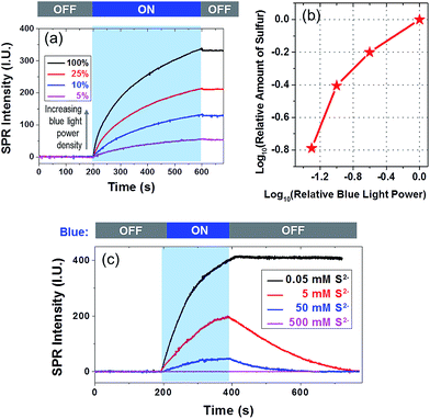
There were two steps involved in a typical sulfur deposition reaction. In the first step, the CdS nanoparticle absorbed incident photons to generate excitons. The gold film facilitated the carrier separation by serving as an electron reservoir. In the second step, remaining holes reacted with surface-adsorbed S2− to produce sulfur deposition. In order to clarify the rate-determining step, we examined the influence of the power density of blue light and [S2−] on the deposition rate, as shown in Fig. 3a and c, respectively. The relationship between power density and the total amount of deposited sulfur is displayed in Fig. 3b on a dual logarithmic scale. The amount of product was dependent on the light intensity at a higher power-law factor (close to 1) when the light intensity was low. When the light intensity was high, the power-law factor decreased and approached 0.5. Such a dependence on the illumination power density has been often observed in semiconductor photocatalysis26,27 because the diffusion of the reactant tends to dominate the reaction rate when the photo-illumination power density is sufficiently high.
The influence of [S2−] on the deposition kinetics was more complicated. A higher [S2−] was expected to increase the reaction rate, and a high concentration of S2− was known to dissolve sulfur via the following reaction S + Na2S = Na2S2, leading to a decreased SPRM intensity. When increasing the [S2−] to 5 and 50 mM, the amount of sulfur deposition was reduced by ∼50% and ∼85%, respectively. No sulfur deposition could be observed at all when [S2−] was 500 mM. Another observation was that the SPRM intensity gradually decreased to the original value in the presence of a high concentration of S2−. Two sulfur dissolution curves (red and blue) were fitted with an exponential function, resulting in rate constants of 0.006 and 0.013 s−1 with [S2−] of 5 and 50 mM, respectively. The dissolution rate increased with an increasing [S2−], which was consistent with the Na2S assisted dissolution of sulfur.
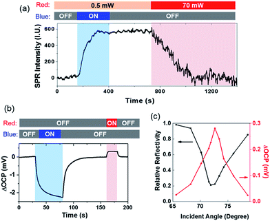
We further investigated the reverse electron transfer from the gold film to the CdS nanoparticle excited by SPPs (Scheme II). After the sulfur deposition, it was found that increasing the power of red light (for generating SPPs) from 0.5 to 70 mW dramatically accelerated the dissolution of sulfur in the presence of 0.05 mM [S2−] (Fig. 4a). The experimental procedure involved a CdS nanoparticle that was illuminated by blue light for 400 s, leading to an increased SPRM intensity due to the deposition of sulfur. The intensity remained unchanged for another 400 s after the removal of blue light. During this period of time (0–800 s), the power density of red light illumination was 0.5 mW (for SPRM imaging). At the 800th s, the power was increased to 70 mW. The SPRM intensity of the particular CdS nanoparticle was found to rapidly decrease to the original value in 300 seconds, demonstrating that the SPPs accelerated the dissolution of sulfur. In this case, red light acted as both the light source (for SPRM imaging) and energy source (for generating hot electrons). A comprehensive movie showing the entire process is also provided in the ESI (Movie S1†). Note that the noise level was also increased on increasing the laser power. In addition, the camera exposure time was correspondingly reduced to obtain a SPRM image with the same overall brightness.
The open circuit potential (OCP) was simultaneously measured to demonstrate the directions of opposite electron transfer when illuminated by blue and red lights (Fig. 4b). An OCP drop was observed under blue illumination, indicating the accumulation of electrons in the gold film. Such an OCP drop has been commonly observed in photoelectrochemical sensing.28 However, the generation of SPPs by illuminating the gold film with a 70 mW red light increased the OCP value, suggesting the depletion of electrons in the gold film. Negative (−2.2 mV) and positive (0.3 mV) OCP changes were recorded for blue and red light illumination, respectively. This result was consistent with the observation that the deposition of sulfur was faster than its dissolution (Fig. 4a). It should be noted that the illumination area of blue light (via condenser) and red light (via objective) was adjusted to be identical (∼100 μm) using apertures.
The incident angle was the key parameter that regulated the efficiency of the coupling of the SPPs.7,8 Therefore, the reflectivity and the OCP change at different incident angles was determined, as shown in Fig. 4c. The reflectivity curve (black) shows a minimal reflectivity at 71.5 deg (i.e., the SPR angle). Coincidently, a maximal OCP increase was also recorded at this angle. A previous study also reported a maximal photocurrent at the angle with minimal reflectivity.11 Such a trend was consistent with the increased rate of sulfur dissolution when the incident angle was close to the SPR angle (Fig. S5†). In addition, a larger OCP increase was also obtained on increasing the power of incident red light (Fig. S6†). These results demonstrated that propagating SPPs were able to excite hot electrons, which were injected into CdS nanoparticles, and resulted in an electrical potential at the Schottky junction in aqueous solution.
Two control experiments were performed to further demonstrate that the dissolution of sulfur was due to the hot electrons excited by SPPs, rather than by the thermal effect. First, the temperature increase due to the dissipation of SPPs at the gold–solution interface was estimated to be ∼10 K using a previously established photothermal technique.29 The incubation of as-deposited CdS@S nanoparticles in a solution at 35 °C for 3 minutes did not lead to observable dissolution of sulfur (Fig. S7†). Second, when setting the incident angle at a non-resonant angle (0 deg), the sulfur did not dissolve on illuminating with the same power of red light (Fig. S7†).
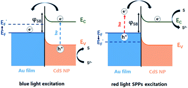
The bidirectional electron transfer mechanisms of the gold film/CdS NP Schottky junctions were elucidated in Fig. 5. On illuminating the interface with blue light, photogenerated electrons from the CdS NP were efficiently transferred to the gold film due to the consumption of holes by S2−, resulting in an increase in the EF of the gold film, which was evidenced by the potential drop of the OCP as indicated in Fig. 4b. In a reverse process, SPPs were generated from the red light at the gold film, resulting in hot electron injection to the conduction band of the CdS nanoparticle, facilitating the reduction of deposited S back to S2−. The consumption of hot electrons, or the accumulation of holes at the gold film, could reduce the EF of the gold film. As a result, the OCP of the Au film increased on illuminating with red light (Fig. 4b).
Conclusions
In conclusion, the visualization of the dynamic processes of SPPs involved in bidirectional electron transfer crossing the metal/semiconductor interface was achieved by monitoring the deposition and dissolution of sulfur at the surface of a single CdS nanoparticle with SPRM. Compared with LSPR contributed by an ensemble of Au or Ag nanomaterials, SPPs excited in the planar gold film were well-defined in both theoretical and experimental frameworks. Moreover, it can be readily regulated by adjusting the optical and geometrical parameters. At the same time, the morphology and chemical composition of the semiconductor can be comprehensively characterized, facilitating the systematic investigations on electron transfer in Schottky junctions. These advantages are anticipated to promote the understanding of the electron transfer mechanisms at metal–semiconductor interfaces, with great implications on photocatalysis, photovoltaic applications and photoelectrochemical sensing.Acknowledgements
We acknowledge financial support from the National Natural Science Foundation of China (NSFC, Grant No. 21522503, 21527807, 21327902, 21327008, 21605078), and the Natural Science Foundation of Jiangsu Province (BK20150013, BK20140592, BK20150570).Notes and references
- C. Clavero, Nat. Photonics, 2014, 8, 95–103 CrossRef CAS.
- S. Linic, P. Christopher and D. B. Ingram, Nat. Mater., 2011, 10, 911–921 CrossRef CAS PubMed.
- Y. Qu and X. Duan, Chem. Soc. Rev., 2013, 42, 2568–2580 RSC.
- C. G. Silva, R. Juarez, T. Marino, R. Molinari and H. Garcia, J. Am. Chem. Soc., 2011, 133, 595–602 CrossRef PubMed.
- D. B. Ingram and S. Linic, J. Am. Chem. Soc., 2011, 133, 5202–5205 CrossRef CAS PubMed.
- J. Yang, D. Wang, H. Han and C. Li, Acc. Chem. Res., 2013, 46, 1900–1909 CrossRef CAS PubMed.
- J. M. Pitarke, V. M. Silkin, E. V. Chulkov and P. M. Echenique, Rep. Prog. Phys., 2007, 70, 1–87 CrossRef CAS.
- J. X. Zhang, L. D. Zhang and W. Xu, J. Phys. D: Appl. Phys., 2012, 45, 113001 CrossRef.
- M. Bernardi, J. Mustafa, J. B. Neaton and S. G. Louie, Nat. Commun., 2015, 6, 7044–7052 CrossRef CAS.
- R. Sundararaman, P. Narang, A. S. Jermyn, W. A. Goddard and H. A. Atwater, Nat. Commun., 2014, 5, 5788–5795 CrossRef CAS PubMed.
- F. M. Wang and N. A. Melosh, Nano Lett., 2011, 11, 5426–5430 CrossRef CAS PubMed.
- A. Giugni, B. Torre, A. Toma, M. Francardi, M. Malerba, A. Alabastri, R. P. Zaccaria, M. I. Stockman and E. Di Fabrizio, Nat. Nanotechnol., 2013, 8, 845–852 CrossRef CAS PubMed.
- P. Andrew and W. L. Barnes, Science, 2004, 306, 1002–1006 CrossRef CAS PubMed.
- J. S. DuChene, B. C. Sweeny, A. C. Johnston-Peck, D. Su, E. A. Stach and D. Wei, Angew. Chem., Int. Ed., 2014, 126, 8021–8025 CrossRef.
- M. T. Sheldon, J. van de Groep, A. M. Brown, A. Polman and H. A. Atwater, Science, 2014, 346, 828–831 CrossRef CAS PubMed.
- K. F. Wu, Z. Y. Chen, H. J. Lv, H. M. Zhu, C. L. Hill and T. Q. Lian, J. Am. Chem. Soc., 2014, 136, 7708–7716 CrossRef CAS PubMed.
- B. Huang, F. Yu and R. N. Zare, Anal. Chem., 2007, 79, 2979–2983 CrossRef CAS PubMed.
- A. Demetriadou and A. A. Kornyshev, New J. Phys., 2015, 17, 1367–2630 CrossRef.
- X. N. Shan, I. Diez-Perez, L. J. Wang, P. Wiktor, Y. Gu, L. H. Zhang, W. Wang, J. Lu, S. P. Wang, Q. H. Gong, J. H. Li and N. J. Tao, Nat. Nanotechnol., 2012, 7, 668–672 CrossRef CAS PubMed.
- Y. M. Fang, W. Wang, X. Wo, Y. S. Luo, S. W. Yin, Y. X. Wang, X. N. Shan and N. J. Tao, J. Am. Chem. Soc., 2014, 136, 12584–12587 CrossRef CAS PubMed.
- A. R. Halpern, J. B. Wood, Y. Wang and R. M. Corn, ACS Nano, 2014, 8, 1022–1030 CrossRef CAS PubMed.
- W. Wang, K. Foley, X. Shan, S. P. Wang, S. Eaton, V. J. Nagaraj, P. Wiktor, U. Patel and N. J. Tao, Nat. Chem., 2011, 3, 249–255 CAS.
- W. Wang, Y. Z. Yang, S. P. Wang, V. J. Nagaraj, Q. Liu, J. Wu and N. J. Tao, Nat. Chem., 2012, 4, 846–853 CrossRef CAS PubMed.
- D. Jiang, Y. Jiang, Z. Li, T. Liu, X. Wo, Y. Fang, N. Tao, W. Wang and H.-Y. Chen, J. Am. Chem. Soc., 2017, 139, 186–192 CrossRef CAS PubMed.
- H. J. Yan, J. H. Yang, G. J. Ma, G. P. Wu, Z. X. Ong, Z. B. Lei, J. Y. Shi and C. Li, J. Catal., 2009, 266, 165–168 CrossRef CAS.
- D. F. Ollis, E. Pelizzetti and N. Serpone, Environ. Sci. Technol., 1991, 25, 1522–1529 CrossRef CAS.
- R. Dillert, A. Engel, J. Grosse, P. Lindner and D. W. Bahnemann, Phys. Chem. Chem. Phys., 2013, 15, 20876–20886 RSC.
- W.-W. Zhao, J.-J. Xu and H.-Y. Chen, Chem. Rev., 2014, 114, 7421–7441 CrossRef CAS PubMed.
- Z. Chen, X. Shan, Y. Guan, S. Wang, J.-J. Zhu and N. Tao, ACS Nano, 2015, 9, 11574–11581 CrossRef CAS PubMed.
Footnotes |
| † Electronic supplementary information (ESI) available: Experimental details, data analysis, control experiment of CdS nanoparticles, descriptions of movies. See DOI: 10.1039/c7sc00990a |
| ‡ These authors contributed equally. |
| This journal is © The Royal Society of Chemistry 2017 |

