Shape-controlled synthesis of single-crystalline anatase TiO2 micro/nanoarchitectures for efficient dye-sensitized solar cells†
Yong
Ding‡
ab,
Tingting
Zhang‡
cd,
Cheng
Liu
a,
Yi
Yang
a,
Jiahong
Pan
a,
Jianxi
Yao
a,
Linhua
Hu
*b and
Songyuan
Dai
 *ab
*ab
aBeijing Key Laboratory of Novel Thin-Film Solar Cells, North China Electric Power University, Beijing, 102206, P. R. China. E-mail: solarhu@sina.com; sydai@ipp.cas.cn
bKey Laboratory of Novel Thin Film Solar Cells, Institute of Applied Technology, Hefei Institutes of Physical Science, Chinese Academy of Sciences, Hefei 230031, P. R. China
cBeijing National Laboratory for Condensed Matter Physics and Institute of Physics, Chinese Academy of Sciences, Beijing 100190, China
dSchool of Physics, Beijing Institute of Technology, Beijing 100081, China
First published on 12th January 2017
Abstract
Single-crystal anatase TiO2 nanocrystals were assembled into different morphological TiO2 micro/nanoarchitectures, including TiO2 hollow microspheres (HM), solid microspheres (SM), and diamond-shaped nanocrystals (NR), by well-controlled solvothermal reactions. The morphology of the resultant TiO2 micro/nanoarchitectures, along with the micro/nanostructural shape, size and crystallinity, can be controlled by varying the concentration of the reactants. It was found that the formation process of TiO2 hollow microspheres might include the hydrolysis of titanium alkoxide with water from the Mannich reaction, the aggregation of TiO2 nanocrystals, the anisotropic crystal growth, and the Ostwald ripening. In addition, we have performed systematic density functional theory (DFT) calculations on the adsorption energy of ethylenediamine molecules on the exposed surfaces and investigated the formation mechanism of single-crystalline nanocrystals. Furthermore, the three TiO2 micro/nanoarchitectures (SM, HM, and NR) were used as photoanode materials in dye-sensitized solar cells (DSSCs) and demonstrated improved light harvesting efficiency and electron collection efficiency, which were much greater than conventional TiO2 nanoparticles under the same conditions. Combined with the large specific surface area and high light scattering ability, the HM-based photoanode achieves the highest power conversion efficiency of 10.66%. Meanwhile, our method provides a versatility for structural engineering of various targeted morphological products to prepare high performance photovoltaic device.
1. Introduction
Owing to their fundamental importance and wide ranging industrial applications, tailored synthesis of well-faceted single crystals of anatase TiO2 micro/nanoarchitectures has aroused great interest.1–4 The preparation of TiO2 single crystals with directional and shape dependence has been a well-known challenge because they usually have large formation energies and their occurrence is naturally inhibited to minimize the overall surface energy of the crystal. To overcome this, one useful approach is to use selective surfactants to adsorb onto specific crystalline facets, which could enhance or reduce surface energies and therefore control crystal growth rates.5–7Recently, T. O. Do et al.8 have shown that the shape evolution of TiO2 nanocrystals from spherical and rhombic structures to rods, dots, dog-bones, and bars could be synthesized by employing both oleic acid and oleylamine to modulate the surface energies of different crystallographic faces, which is the key parameter for shape control. A. Adachi et al.9 have demonstrated that the formation of single-crystal anatase TiO2 nanowires could be realized by using organic molecules as surface ligands that probably adsorb selectively to the specific surface planes. However, there were few reports on the fine control of single-crystal TiO2 nanocrystals assembled into three-dimensional hierarchical architectures, especially solid or hollow micro/nanoarchitectures.10–12 Starting around 2001,13 there has been a large increase in research about solid or hollow micro/nanoarchitectures based on template methods, including conventional hard templates,14,15 soft templates16 and sacrificial templates.17 These methods are advantageous in terms of effective and versatile synthesis of micro/nanoarchitectures, but disadvantageous because of the low yield, high cost and tedious synthetic procedures. To explore the tailored synthesis of TiO2 micro/nanoarchitectures, a continuous and scalable synthesis method that allows precise control over the shape, size and crystallinity of micro/nanoarchitectural structures is required. Therefore, template-free methods with the aid of selective surfactants, based on the mechanism of inside-out Ostwald ripening,18 have been developed for customizing TiO2 micro/nanoarchitectural materials.
Herein, different morphological TiO2 micro/nanoarchitectures self-assembled by single-crystalline nanocrystals were synthesized by a facile solvothermal method in a nonaqueous mixture solution of acetone and isopropanol with the assistance of ethylenediamine. The central features of our method are on the basis of Mannich reactions19 to slow the hydrolysis rate and ethylenediamine as a selective surfactant to control the growth of TiO2 nanocrystals from nearly spherical to slender nanocrystals and to a truncated rhombic shape. The reaction mechanism and formation process are proposed to elucidate the effect of the reaction parameters on the morphology of the products. Based on the density functional theory (DFT) calculations, the amine functional groups of ethylenediamine have been proven to tightly bind on the TiO2 surface and led to the formation of single crystalline TiO2 nanocrystals. Because of the decreased inter-crystalline contacts between grain boundaries and stretched grown structure to the specific directionality, single-crystal TiO2 nanocrystals assembled into TiO2 hollow microspheres could greatly enhance the electron collection efficiency by the favorable electron transport and reduced electron recombination. Along with the high specific area and light scattering effect, the TiO2 hollow microsphere-based DSSC achieves the highest power conversion efficiency of 10.66%, indicating a 12.3% improvement of the TiO2 nanoparticle-based DSSC. This work not only provides an efficient route to synthesize TiO2 micro/nanoarchitecture with complementary and synergistic properties for high performance of photovoltaic performance, but also gives insight into understanding of the anisotropic crystal growth behavior of single-crystal nanocrystals, which can be extended to the shape-controlled synthesis of other transition metal oxides.
2. Experimental section
2.1. Materials and synthesis
Isopropyl alcohol (IPA), acetone (AC), ethylenediamine (EDA) and tetrabutyl titanate (TBT) were purchased from Sinopharm Chemical Reagent Co., Ltd, and used without further purification. In this study, TiO2 nanoparticles were synthesized by a two-step process: sol–gel and subsequent solvothermal treatment, as described in the previous literature.20 The shape-controlled synthesis of anatase TiO2 was simply carried out by adjusting the experiment parameters. In a typical synthetic procedure, 2–4 mL of TBT, 40 mL IPA, and 10 mL AC were mixed together in a flask under vigorous stirring at ambient temperature for 15 min. Then, EDA (0–2 mL) was injected into the flask, and the mixture was magnetically stirred for another 15 min to ensure homogeneity. On increasing the volume of EDA from 0 mL to 0.5 mL and to 1.0 mL, the color of solution changes from colorless to pale yellow and to slightly turbid, respectively, indicating the formation of a complex. Subsequently, the obtained solution was transferred to a 100 mL Teflon-lined autoclave, which was then heated at 200 °C for 24 h. After the autoclave cooled to ambient temperature, the as-obtained product was washed with ethanol several times.2.2. Device fabrication
The pastes of TiO2 nanoparticles and micro/nanoarchitectures were prepared as described elsewhere,4,18,20 as follows. These crystallographic microspheres (5.0 g) were redispersed in the ethanol suspension, containing 1.0 g ethyl cellulose and 25.0 g α-terpineol. These pastes were prepared by using rotary evaporation to remove the excess volatile ethanol solvent and a three-roll grinder to obtain a uniform paste. TiO2 pastes were then screen-printed on the FTO glass (15 Ω sq−1) and then sintered in air at 510 °C for 30 min. The thickness of the films measured by using a profilometer (XP-2, AMBIOS Technology, Inc., USA) was about 9.5 μm. Prior to sensitization, the films were soaked into 0.05 M TiCl4 aqueous solution and stored in a closed container at 70 °C for 30 min. After washing and re-sintering, these films were immersed into a 300 μM C101 dye with cheno-3a, 7a-dihydroxy-5b-cholic acid for the whole night. After being washed with acetonitrile and dried in air, the sensitized photoanodes were assembled with a Pt-modified counter electrode and a high-efficiency electrolyte (30 mM I2, 50 mM LiI, 1 M 1,3-dimethylimidazolium iodide (DMII), 0.5 M tert-butylpyridine, and 0.1 M guanidinium thiocyanate (GuSCN) in a solvent mixture of 85% acetonitrile with 15% valeronitrile by volume) by using a laser engraved 60 μm Surlyn gasket under heat and pressure.2.3. Materials and photovoltaic characterization
The morphologies of shape-controlled TiO2 were investigated by using scanning electron microscopy (SEM, S-4800, HITACHI, Japan) and field emission transmission electron microscopy (FE-TEM, JEM-2100F, JEOL, Japan). Powder X-ray diffraction (XRD, MXPAHF, Mark Corp., Japan) was used to determine the crystalline phase and calculate crystal sizes of the samples. Fourier transform infrared (FTIR) spectra were recorded with a Thermo Scientific Nicolet IS50-Nicolet FTIR spectrophotometer in the range of 4000–1000 cm−1 with KBr plates. The Brunauer–Emmett–Teller (BET) surface area and pore size distribution were evaluated by using a micromeritics (TriStar II 3020 V1.03, Micromeritics Instrument Corporation) nitrogen adsorption/desorption apparatus. UV-vis diffuse reflection spectra were obtained from a UV-vis spectrophotometer (SOLID 3700, Shimadzu Co. Ltd, Japan) to measure the diffuse reflectance of films without adsorbing dyes. Dye loading of the films prior to TiCl4 treatment was measured on this spectrophotometer after desorbing the dye with a 63 mM solution of tetrabutylammonium hydroxide (TBAH) in dimethyl formamide (DMF) for 15 min. The absorption peak at 540 nm was used to calculate the number of adsorbed C101 dye molecules, according to the Beer–Lambert law, defined as follows:| Aabs = εbc | (1) |
The current density–voltage (J–V) measurements were performed on a Keithley 2420 digital source meter (Keithley, USA), and controlled by using Test point software under a 450 W xenon lamp (Orial, USA) with a filter (AM 1.5, 100 mW cm−2). The incident light intensity was calibrated with a standard crystalline silicon solar cell before each experiment, and the lamp spectra are provided in the ESI (Fig. S1†). The active area of photoanodes, determined by the aperture of a black mask, was 0.16 cm2. The incident photon-to-current conversion (IPCE) values were confirmed as a function of wavelength from 300 to 800 nm (PV Measurements, Inc.) for DSSCs. An electrochemical workstation (IM6e, Zahner, Germany) was conducted to measure the intensity of the modulated photocurrent/photovoltage spectroscopy (IMPS/IMVS) with light emitting diodes (LED, λ = 610 nm) driven by Export (Zahner, Germany). The small amplitude is 10% or less than that of the dc component provided by the LED, and the frequency range was from 300 mHz to 3 kHz.
2.4. Density functional theory calculations
The calculations were based on the density functional theory (DFT). DFT modelling details: all DFT calculations on adsorption energy were carried out using Vienna Ab Initio Simulation Program (VASP) with the projector augmented wave (PAW) method.21,22 The generalized gradient approximation (GGA) formulated by Perdew, Burke and Ernzerhof (PBE) was employed for the exchange and correlation effects. The energy cutoff of the plane wave basis was set to 400 eV and a 2 × 2 × 1 k-point mesh was used for the Brillouin zone sampling. Four layers of TiO2 were considered as the surface of TiO2 with the bottom two layers fixed and the surface two layers fully relaxed in all calculations. All structures were optimized until the force on each atom was less than 0.05 eV Å−1.3. Results and discussion
3.1. Effects of TBT
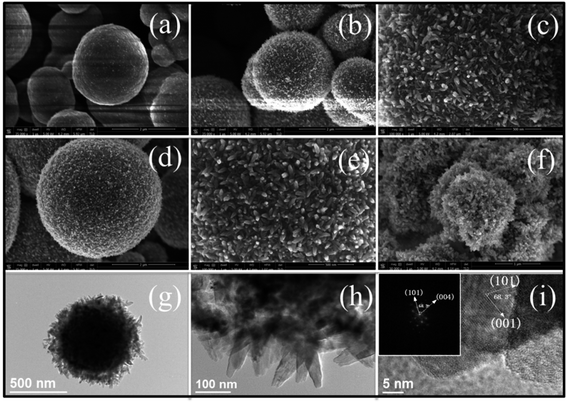
Fig. 1 shows the morphological evolutions when the volume of TBT is 2 mL and EDA is 0.5 mL under different reaction times. After the solvothermal reaction for 4 h, smooth TiO2 solid microspheres (SM) consisting of tiny nanoparticles were obtained (Fig. 1a). With a further increase of reaction time to 8 h, smooth microspheres are transformed into rough microspheres with rod-shaped nanocrystals (Fig. 1b and c). Each nanocrystal has a fairly homogeneous rhombic texture. The rhombic texture nanocrystals tend to grow along the radial direction, and the slender nanocrystals are produced (Fig. 1d and e). By prolonging the reaction time to 24 h, the SM with ∼800 nm size is formed accompanied by the growth of nanocrystals in the microspheres (Fig. 1f). The above observations can be further determined by the corresponding TEM images (Fig. S2†). By prolonging the reaction time during solvothermal treatment, the nanocrystals at the surface of the SM grow larger. In addition, as confirmed by the XRD pattern (Fig. S3†), the diffraction peaks become sharper, corresponding to the growth of TiO2 nanocrystals. Their sizes, estimated from the (101) diffraction peak based on the Scherrer equation, are calculated to be 20 nm, 24 nm, 27 nm and 35 nm, confirming the trend observed by SEM and TEM.The TEM image (Fig. 1g) shows that the core in the SM is dense while the shell composed of nanocrystals is relatively loose, which could facilitate the dye adsorption and electrolyte diffusion in the DSSCs. These nanocrystals in the shell (Fig. 1h) are ∼40 nm in width and over 200 nm in length, in accordance with the observation from the above SEM images. The high-resolved TEM (HRTEM) image (Fig. 1i) demonstrates that the interplanar spacings of short nanocrystals are 0.352 and 0.480 nm, corresponding to the (101) and (002) facets of anatase TiO2, respectively. An interfacial angle of 68.3° matches well with the theoretical value.23 The same interfacial angle can be observed by the corresponding fast Fourier transform (FFT) pattern shown in the inset in Fig. 1i. The nanocrystals were elongated along the [001] direction, and the long axis of the rods is parallel to the [001] direction.
By doubling the volume of TBT and unchanging the volume of EDA, TiO2 hollow microspheres (HM, Fig. 2a and b) with a diameter of 800–1200 nm are produced. Their hollow interior is clearly uncovered with some broken microspheres, and can be further confirmed by TEM analysis (Fig. 2c). The spherical shells of HM composed of radial nanocrystals are similar to the SM. These nanocrystals are mutually interconnected and have interlocking features on the shell of HM, which provide more efficient electron transport pathways than the less-organized nanoparticle-based nanostructure.24 It is noteworthy that the single HM is a core/shell structure and the thickness of the shell is about 100 nm. The 40 nm in width and 80–100 nm in length of nanocrystals can be represented as in Fig. 2d. Each nanocrystal possesses (001), (101) and (−101) facets, indicating that the nanocrystal presents a single-crystal nature with an elongated crystalline domain in the c-axis direction. Therefore, originally attacked features of TiO2 elongated nanocrystals assembled into microspheres, such as the reduced inter-crystalline contacts between grain boundaries and stretched grown structure, can make a favorable contribution to the electron transport.25
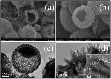 | ||
| Fig. 2 SEM images (a and b) and TEM images (c and d) of TiO2 hollow microspheres (HM). Inset in (d): high-resolution TEM image of the corresponding HM. | ||
Tuning the dosage of TBT allows the facile control of the inner structure of the resulting TiO2 microspheres. To further verify the role of TBT and understand the hollowing process, a continuous morphological evolution of the HM during the solvothermal reaction was investigated. As shown in Fig. 3a, the initial state of the reaction is solid microspheres. Interestingly, after 4 h, the asymmetrical hollowing process starts from the side of the microsphere beneath the shell, which divides the pristine solid microsphere into two discrete regions and forms a core–shell structure (Fig. 3b). The solid cores gradually shrink, while the shells grow up with time (Fig. 3c). The solid microspheres developed into the above homogeneous core/shell structure might be ascribed to the intrinsic size/density variations between the outer and inner structure.
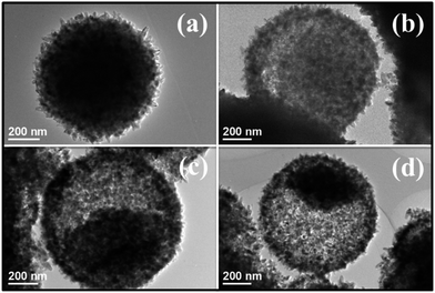 | ||
| Fig. 3 Typical TEM images of the HM synthesized with reaction durations of (a) 4 h, (b) 8 h, (c) 12 h, and (d) 24 h. | ||
It is supposed that the higher volume of TBT leads to the faster nucleation and generates smaller nanocrystals (at a fast rate under initial high supersaturation). To minimize the interfacial energy, these tiny nanocrystals are prone to aggregate into solid microspheres. During the aggregation process, nanocrystals situated in the outermost surface would act as starting points for the subsequent recrystallization process. As evidenced by TEM image in Fig. 3a, the outer nanocrystals grow into larger nanocrystals on attracting the smaller nanocrystals underneath (at a slow rate under low supersaturation). However, smaller nanocrystals underneath possess higher surface energies, and their surface energies are higher than the surrounding solution, giving rise to having a strong tendency to dissolve and diffuse out through the shell.11,26 Afterward, the solid microspheres are further crystallized and finally transform into a core/shell structure (Fig. 3d), which follows the typical asymmetrical Ostwald ripening mechanism.27
3.2. Effects of EDA
The EDA also acts as a strong base involved in the Mannich reaction with acetone to produce the Schiff base and water molecule,19,28 as illustrated in eqn (2):| CH3COCH3 + H2NCH2CH2NH2 → (CH3)2CNCH2CH2NH2 + H2O | (2) |
| Ti(OBu)4 + H2O → Ti(OBu)3OH + BuOH | (3) |
| Ti(OBu)3OH + Ti(OBu)3OH → (OBu)3Ti–O–Ti(OBu)3 + H2O | (4) |
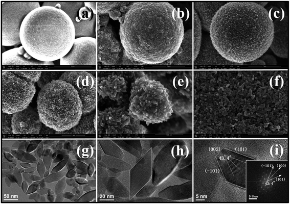
Fig. 4 shows the morphology evolution of TiO2 micro/nanoarchitectures synthesized by increasing the volume of EDA and leaving the volume of TBT unchanged. Without the addition of EDA, 5 μm-sized microspheres composed of irregular spherical nanoparticles are obtained (Fig. 4a). When 0.25 mL of EDA is added, the diameter of microspheres decreases to 3 μm, and the surface of microspheres becomes rough (Fig. 4b). A further increase in the volume of EDA (0.5 mL and 0.75 mL) leads to a decrease in the diameter of microspheres, and its nanocrystal shape evolves from a tiny granule-like to a slightly elongated rod-like structure (Fig. 4c and d, respectively). When the volume of EDA is increased up to 1.0 mL, the formation of 500 nm-sized microspheres is observed with diameters of 20–30 nm and lengths of over 100 nm (Fig. 4e). This is because of the large amount of EDA used where the reactions (3) and (4) are accelerated, leading to decreasing diameters of microspheres, whereas, XRD patterns in Fig. S4† demonstrate that the relative (004)/(200) intensity is gradually increased as the nanocrystal shape evolves from tiny spherical granule to elongated nanocrystals. The differences in the peak intensity of (004) and (200), pointing to c-axis and a-axis, respectively, are usually correlated with the typical anisotropic growth pattern.
It is well-known that the anisotropic crystal growth is conducive to the formation of elongated nanocrystals, which often occurs when the surface free energies of different crystal faces are different significantly. The equilibrium morphology of anatase TiO2 is a truncated tetragonal bipyramid shape enclosed with eight equivalent (101) faces and two equivalent (001) faces. According to the Wulff's theorem, the average surface energy of the (001) facet (0.9 J m−2) was reported to be 2.04 times larger than that for the (101) facet (0.44 J m−2), indicating an intrinsic of crystal growth rates.29 The use of different surfactants has been reported as an efficient approach for enhancing or reducing the surface free energy by surfactant adhesion.6 In our mono-surfactant system, the EDA molecule is a typical bridging ligand in which each end of the molecule contains a base group that might form a chemical bond with the acid surface atoms through a donor–acceptor mechanism.22 The relatively stable Ti4+–EDA complexes may be formed through the adsorption of the EDA onto titanium and/or titanium oxides, which might change the relative surface free energies of the (001) and (101) faces and, therefore, the growth rate ratio between [001] and [101] directions.6,30
The formation of Ti4+–EDA complexes was studied systematically by using the FTIR spectra (Fig. S5†), which provides information on surface functional groups. The FTIR spectrum displays a broadband centering at 3440 cm−1 and other bands at 1630 cm−1 and 1385 cm−1. The broadband centering at 3440 cm−1 and 1630 cm−1 could be attributed to surface adsorbed water and the bending vibration of the O–H group, respectively.31 A new feature at 1385 cm−1 in the presence of EDA, assigned to the bending vibration of the N–H group, indicates the coordination of EDA to titanium centers to form Ti4+–EDA complexes.32
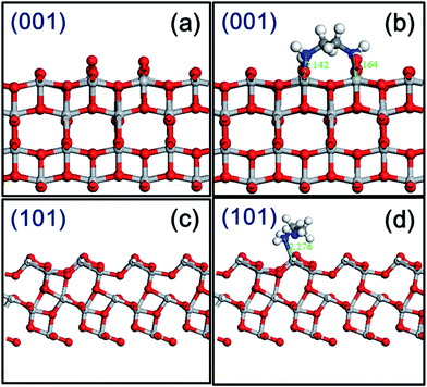
To better understand the EDA molecule–surface interactions, studies on model systems have been performed, generally on the (001) and (101) facets of anatase TiO2. As shown in Fig. S6† and 5, the most stable configuration for EDA adsorbed on the TiO2 surface is through N in bond with Ti atom with a N–Ti bond length of 2.14–2.28 Å. In modeling the adsorption phenomenon, we calculated the adsorption energy (Ebinding), defined as follows:
| Ebinding = EEDA–facet − EEDA − Efacet | (5) |
| Ebinding = EEDA–(001) − EEDA − E(001) = −4.38 eV |
| Ebinding = EEDA–(101) − EEDA − E(101) = −1.99 eV |
The binding energy of the EDA on the (001) facet is much stronger than on the (101) facet with a decreased Ti–N bond length. Thus, the favorable surface is the (001) facet of anatase TiO2 upon EDA adsorption, where two Ti–N bonds are formed.7
At low EDA contents, crystal growth is predominant in the system. During the growth of TiO2 nanocrystals, the shape of nanocrystals is determined by the growth rate ratio between [001] and [101] directions. Due to the high surface energy of the (001) facet, growth along the [001] direction is occurring progressively, thus generating the elongated nanocrystals. However, with a further increase of the EDA content to 2 mL, the length of the nanocrystal decreases to 60 nm, indicating a suppression of anisotropic growth at high EDA contents. Moreover, only truncated rhombic TiO2 nanocrystals (NRs, Fig. 4f) were obtained resulting from the increased structural stress. Under high structural stress, all microspheres collapse into isolated nanocrystals.34 As revealed by low-magnification TEM images in Fig. 4g and h, the NR consists of high aspect ratio nanocrystals, having a uniform diameter of 20–30 nm and length up to 60 nm. A HRTEM image focused on a single nanocrystal in Fig. 4i reveals that the top and side surfaces of the nanocrystal are the (001) and (101) facets, respectively. The angle labeled in the corresponding FFT image is 43.4°, which is identical to the theoretical value of the angle between the (101) and (100) facets. As shown in Fig. S4,† these individual nanocrystals give an intensity ratio of (004)/(200) of as high as 1.11, which is larger than that with a low volume of EDA. These nanocrystals are inhibited in a range of short length with the same diameter, which provides clues for shape control in nanocrystal formation with excess EDA. A similar observation was also reported by M. Adachi et al.25 using cetyltrimethylammonium bromide (CTAB) as the surface selective surfactant. Therefore, it can be concluded that the shape of nanocrystals can be controlled by adjusting the growth rate ratio between [001] and [101] directions via regulating the contents of surfactant molecules and can make a single crystalline anatase exposed with the (001) facet.
3.3. Photovoltaic performance
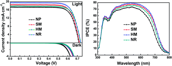
In order to study the effects of morphologies on the photovoltaic performance of DSSCs, three typical samples with morphologies of SM, HM and NR were chosen as photoanode materials in DSSCs. The current density–voltage (J–V) curves and relevant photovoltaic parameters (including short-circuit current density (Jsc), open-circuit voltage (Voc), fill factor (FF) and the power conversion efficiency (η)) are shown in Fig. 6a and are summarized in Table 1. As a reference for comparison, 18 nm sized nanoparticle (NP) based photoanodes with a similar thickness were assembled into DSSCs. The four DSSCs have a similar FF, however, the Voc increases gradually from NP, SM, HM to NR-based cells. The systematic trend for the dark current of the four cells decreased in the order of NP > SM > HM > NR. The lower the dark current, the more the charge recombination and thus the higher the Voc.35 The Jsc varies rapidly from 17.37 for the NP sample, 18.54 for SM, 19.52 for HM, to 17.91 mA cm−2 for the NR cell. Therefore, the η varies automatically from 9.32% for the NP sample to 10.00% for the SM, 10.66% for the HM and 9.86% for the NR cell.| Cell | V oc (V) | J sc (mA cm−2) | FF | η (%) | Absorbed dye (×10−7 mol cm−2) |
|---|---|---|---|---|---|
| NP | 0.715 | 17.37 | 0.751 | 9.32 | 1.91 |
| SM | 0.720 | 18.54 | 0.749 | 10.00 | 1.97 |
| HM | 0.732 | 19.52 | 0.746 | 10.66 | 2.15 |
| NR | 0.734 | 17.91 | 0.750 | 9.86 | 1.87 |
It is well-known that the Jsc can be explained by the following equation:
| Jsc = q × IPCE(λ) × I0 | (6) |
| IPCE(λ) = LHE(λ)φinjηc | (7) |
Fig. S8† shows the diffused reflectance spectra of SM, HM and NR films, along with the NP film. The reflectance of SM and HM films is higher than that of the NP and NR films, indicating that the former two films have a higher light scattering ability than the latter two films due to the Mie effect.18 In addition, the multiple reflection and scattering between the core and shell of the HM could trap the incident light and reinforce the reflectivity.37 The highest reflectance is therefore found in the HM, followed by the SM, NR and NP. Considering the synergic effect of the dye loading and light scattering in the four photoanodes, the HM photoanode is expected to have the highest LHE(λ) than the other three photoanodes.38
Intensity-modulated photocurrent/photovoltage spectroscopy (IMPS/IMVS) have been performed to quantificationally investigate the electron transport and recombination of DSSCs in these four different photoanodes. The transport time (τd) and electron lifetime (τn) can be calculated from the expression: τd = 1/2πfd and τn = 1/2πfn, respectively, where fd and fn are the frequencies for which the imaginary components of IMPS and IMVS reach a minimum, respectively.39 For the kinetics of electron transport and recombination of the devices, τn and τd are defined as the time constant of recombination with I3− in the electrolyte and injected electron transport through the photoanodes, respectively. Fig. 7 displays the τn and τd as a function of light intensity. It is noticed that the τn values of NR are slightly higher than those of the HM and SM-based cell, but much larger than that of the NP-based cell when compared at the same light intensity level, indicating that electron recombination is relatively more suppressed at the NR photoanode/electrolyte interface. This is attributed to the high crystallinity and compact packing of truncated rhombic-shape TiO2 nanocrystals in the NR film.40,41 However, the poor contact between the adjacent microspheres in the HM and SM photoanodes provides more trapping sites for recombination with I3− in the electrolyte, leading to a slightly inferior electron lifetime and thus a decreased Voc.42
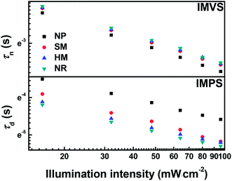 | ||
| Fig. 7 Electron lifetime (IMVS) and electron transport time (IMPS) as a function of light intensities for the DSSCs based on the NP, SM, HM, and NR photoanodes. | ||
One can notice that the τd values of the NR and HM-based cells are similar but much shorter than those based on SM and NP-based cells under the same light irradiation, implying the faster electron transport of the former. This significant improvement of electron transport might be accounted for as the basic reason of the single crystalline TiO2 nanocrystals, which have a high interior conductivity and interfacial conductivity through the (101) planar contacts between nanocrystals.43 In addition, the HM with a certain amount of fractured nanocrystals demonstrated above by SEM and TEM could enhance the interior conductivity by forming a highway to facilitate electron transport.44 It is presumed that the interlaced and interconnected network of primary building blocks with the single-crystal nanocrystals brings about a synergistic effect for accelerated electron transport and suppressed electron recombination. Therefore, the NR and HM-based cells achieve high electron collection efficiency, followed by the SM and NP-based cells.
By comprehensive analysis of the LHE(λ) and ηc trends for the four kinds of photoanodes, there is no doubt on the IPCE sequence of HM > SM > NP-based cells (Fig. 6b). Only question left is the position of the NR-based cell. It might be because of the fact that its inferior LHE(λ) offsets the prominent ηc. Therefore, it is reasonable to conclude that the HM-based cell possesses the dual effects of superior light harvesting efficiency and electron collection efficiency.
4. Conclusions
In summary, different morphologies of anatase TiO2 from solid microspheres (SM), hollow microspheres (HM) and truncated rhombic-shape nanocrystals (NR) have been successfully synthesized by simply adjusting the volume ratio of tetrabutyl titanate to ethylenediamine in the presence of isopropyl alcohol and acetone. Systematic investigations of different experimental conditions disclose the mechanism of morphological variations from SM, HM to NR. By controlling the hydrolysis and condensation step, TiO2 solid microspheres have been transformed into hollow microspheres, while the ethylenediamine served as a selective surfactant, which plays an important role in tailoring the size and shape of TiO2 primary nanocrystals. In addition, the role of ethylenediamine was explored by density functional theory calculations, revealing that surface energy control by surfactant molecules is an effective way for tailoring the nanocrystal shape. Favorable properties of the HM, such as single-crystal crystallinity, high specific surface area, efficient light scattering and superior electron transport, allow them to be demonstrated as suitable photoanode materials for improving the light harvesting efficiency, accelerating the electron transport and restraining the electron recombination to significantly enhance the photovoltaic performance of DSSCs. As expected, the HM-based cell achieves the highest power conversion efficiency of 10.66%.Acknowledgements
This work was supported by the National Natural Science Foundation of China (No. 51572080 and 61404142), the National High Technology Research and Development Program of China (No. 2015AA050602), and the National Key Basic Research Program of China (973 Program) (No. 2015CB932201).References
- S. H. Kang, S. H. Choi, M. S. Kang, J. Y. Kim, H. S. Kim, T. Hyeon and Y. E. Sung, Adv. Mater., 2008, 20, 54–58 CrossRef CAS.
- X. Wu, Z. G. Chen, G. Q. Lu and L. Z. Wang, Adv. Funct. Mater., 2011, 21, 4167–4172 CrossRef CAS.
- M. Liu, L. Piao, L. Zhao, S. Ju, Z. Yan, T. He, C. Zhou and W. Wang, Chem. Commun., 2010, 46, 1664–1666 RSC.
- Y. Ding, L. Zhou, L. e. Mo, L. Jiang, L. Hu, Z. Li, S. Chen and S. Dai, Adv. Funct. Mater., 2015, 25, 5946–5953 CrossRef CAS.
- Z. Zhang, X. Zhong, S. Liu, D. Li and M. Han, Angew. Chem., Int. Ed., 2005, 44, 3466–3470 CrossRef CAS PubMed.
- Y. W. Jun, M. F. Casula, J. H. Sim, S. Y. Kim, J. Cheon and A. P. Alivisatos, J. Am. Chem. Soc., 2003, 125, 15981–15985 CrossRef CAS PubMed.
- J. M. Du, J. S. Zhang and D. J. Kang, CrystEngComm, 2011, 13, 4270–4275 RSC.
- C. T. Dinh, T. D. Nguyen, F. Kleitz and T. O. Do, ACS Nano, 2009, 3, 3737–3743 CrossRef CAS PubMed.
- M. Adachi, Y. Murata, J. Takao, J. T. Jiu, M. Sakamoto and F. M. Wang, J. Am. Chem. Soc., 2004, 126, 14943–14949 CrossRef CAS PubMed.
- D. Chen and R. A. Caruso, Adv. Funct. Mater., 2013, 23, 1356–1374 CrossRef CAS.
- X. W. Lou, L. A. Archer and Z. Yang, Adv. Mater., 2008, 20, 3987–4019 CrossRef CAS.
- H. J. Cho and D. Jung, Bull. Korean Chem. Soc., 2011, 32, 4382–4386 CrossRef CAS.
- F. Caruso, X. Y. Shi, R. A. Caruso and A. Susha, Adv. Mater., 2001, 13, 740–744 CrossRef CAS.
- U. Meyer, A. Larsson, H. P. Hentze and R. A. Caruso, Adv. Mater., 2002, 14, 1768–1772 CrossRef CAS.
- C.-Y. Liao, S.-T. Wang, F.-C. Chang, H. P. Wang and H.-P. Lin, J. Phys. Chem. Solids, 2014, 75, 38–41 CrossRef CAS.
- Y. M. Cui, L. Liu, B. Li, X. F. Zhou and N. P. Xu, J. Phys. Chem. C, 2010, 114, 2434–2439 CAS.
- Y. X. Hu, J. P. Ge, Y. G. Sun, T. R. Zhang and Y. D. Yin, Nano Lett., 2007, 7, 1832–1836 CrossRef CAS PubMed.
- Y. Ding, X. Xia, W. Chen, L. Hu, L. e. Mo, Y. Huang and S. Dai, Nano Res., 2016, 9, 1891–1903 CrossRef CAS.
- Y. Jia and J. B. Li, Chem. Rev., 2015, 115, 1597–1621 CrossRef CAS PubMed.
- L. Hu, S. Dai, J. Weng, S. Xiao, Y. Sui, Y. Huang, S. Chen, F. Kong, X. Pan, L. Liang and K. Wang, J. Phys. Chem. B, 2007, 111, 358–362 CrossRef CAS PubMed.
- J. G. Chang, H. T. Chen, S. P. Ju, H. L. Chen and C. C. Hwang, Langmuir, 2010, 26, 4813–4821 CrossRef CAS PubMed.
- A. Hemeryck, A. Motta, J. Swiatowska, C. Pereira-Nabais, P. Marcus and D. Costa, Phys. Chem. Chem. Phys., 2013, 15, 10824–10834 RSC.
- B. Wu, C. Guo, N. Zheng, Z. Xie and G. D. Stucky, J. Am. Chem. Soc., 2008, 130, 17563–17567 CrossRef CAS PubMed.
- S. H. Ahn, D. J. Kim, W. S. Chi and J. H. Kim, Adv. Funct. Mater., 2014, 24, 5037–5044 CrossRef CAS.
- J. Jiu, S. Isoda, F. Wang and M. Adachi, J. Phys. Chem. B, 2006, 110, 2087–2092 CrossRef CAS PubMed.
- B. Liu and H. C. Zeng, Small, 2005, 1, 566–571 CrossRef CAS PubMed.
- C. X. He, B. X. Lei, Y. F. Wang, C. Y. Su, Y. P. Fang and D. B. Kuang, Chem. – Eur. J., 2010, 16, 8757–8761 CrossRef CAS PubMed.
- X. Y. Zhu, C. Chen, B. X. Yu, G. F. Zhang, W. Q. Zhang and Z. W. Gao, Chem. Lett., 2014, 43, 1832–1834 CrossRef.
- H. G. Yang, C. H. Sun, S. Z. Qiao, J. Zou, G. Liu, S. C. Smith, H. M. Cheng and G. Q. Lu, Nature, 2008, 453, 638–641 CrossRef CAS PubMed.
- Z. Zhong, V. Ng, J. Luo, S. P. Teh, J. Teo and A. Gedanken, Langmuir, 2007, 23, 5971–5977 CrossRef CAS PubMed.
- J. Fang, F. Wang, K. Qian, H. Z. Bao, Z. Q. Jiang and W. X. Huang, J. Phys. Chem. C, 2008, 112, 18150–18156 CAS.
- Q. C. Xu, D. V. Wellia, R. Amal, D. W. Liao, S. C. J. Loo and T. T. Y. Tan, Nanoscale, 2010, 2, 1122–1127 RSC.
- L. Triggiani, A. B. Muñoz-García, A. Agostiano and M. Pavone, Theor. Chem. Acc., 2015, 134, 119–130 CrossRef.
- J. H. Pan, X. Z. Wang, Q. Huang, C. Shen, Z. Y. Koh, Q. Wang, A. Engel and D. W. Bahnemann, Adv. Funct. Mater., 2014, 24, 95–104 CrossRef CAS.
- A. Hagfeldt, G. Boschloo, L. C. Sun, L. Kloo and H. Pettersson, Chem. Rev., 2010, 110, 6595–6663 CrossRef CAS PubMed.
- J.-Y. Liao, B.-X. Lei, D.-B. Kuang and C.-Y. Su, Energy Environ. Sci., 2011, 4, 4079–4085 CAS.
- Z. H. Dong, X. Y. Lai, J. E. Halpert, N. L. Yang, L. X. Yi, J. Zhai, D. Wang, Z. Y. Tang and L. Jiang, Adv. Mater., 2012, 24, 1046–1049 CrossRef CAS PubMed.
- S. H. Hwang, J. Yun and J. Jang, Adv. Funct. Mater., 2014, 24, 7619–7626 CrossRef CAS.
- W. Q. Wu, Y. F. Xu, H. S. Rao, C. Y. Su and D. B. Kuang, J. Am. Chem. Soc., 2014, 136, 6437–6445 CrossRef CAS PubMed.
- D. Wu, Y. Wang, H. Dong, F. Zhu, S. Gao, K. Jiang, L. Fu, J. Zhang and D. Xu, Nanoscale, 2013, 5, 324–330 RSC.
- S. R. Gajjela, C. Yap and P. Balaya, J. Mater. Chem., 2012, 22, 10873–10882 RSC.
- Y. Ding, L.-E. Mo, L. Tao, Y.-M. Ma, L.-H. Hu, Y. Huang, X.-Q. Fang, J.-X. Yao, X.-W. Xi and S.-Y. Dai, J. Power Sources, 2014, 272, 1046–1052 CrossRef CAS.
- K. Yan, Y. Qiu, W. Chen, M. Zhang and S. Yang, Energy Environ. Sci., 2011, 4, 2168–2176 CAS.
- J.-Y. Liao, J.-W. He, H. Xu, D.-B. Kuang and C.-Y. Su, J. Mater. Chem., 2012, 22, 7910–7918 RSC.
Footnotes |
| † Electronic supplementary information (ESI) available. See DOI: 10.1039/c6se00041j |
| ‡ These authors contributed equally to this work. |
| This journal is © The Royal Society of Chemistry 2017 |

