Influence of a compact CdS layer on the photovoltaic performance of perovskite-based solar cells
Jun
Wang
a,
Li
Liu
a,
Shurong
Liu
a,
Lihua
Yang
b,
Bowen
Zhang
a,
Shuang
Feng
a,
Jiandong
Yang
a,
Xianwei
Meng
a,
Wuyou
Fu
a and
Haibin
Yang
 *a
*a
aState Key Laboratory of Superhard Materials, Jilin University, Qianjin Street 2699, Changchun, 130012, People's Republic of China. E-mail: yanghb@jlu.edu.cn; Fax: +86 431 85168763; Tel: +86 431 85168763
bCollege of Electronic Science and Engineering, Jilin University, Changchun 130012, PR China
First published on 24th January 2017
Abstract
In this study, a uniform and dense cadmium sulfide (CdS) thin film is utilised as an electron-transport layer in CH3NH3PbI3-based perovskite solar cells (PSCs). CdS films are synthesized by a homogeneous precipitation method in urea aqueous solution. The effect of urea concentration on the growth of CdS films has been investigated. It is noted that increasing urea concentration remarkably affects the grain size and uniformity of the films. A compact CdS thin film with appropriate grain size can be obtained by adding 1.5 M urea. The photovoltaic performance of the PSCs based on the as-prepared CdS films is also studied. The photovoltaic conversion efficiency (PCE) of the PSCs shows a significant dependence on CdS layers. The highest PCE is obtained by using a CdS thin film prepared in 1.5 M urea, which can be attributed to the better coverage of perovskite on the CdS film for efficient charge separation and transport.
1. Introduction
Perovskite-based solar cells (PSCs) have recently drawn increasing attention due to their superior performance and ease of fabrication. Impressive progress in improving the photovoltaic performance has been achieved in this field. The power conversion efficiency (PCE) of PSCs has been incredibly increased to more than 20%.1–6 To better understand the material properties and the device working mechanisms, simplified planar heterojunction structured devices have become the focus of many research endeavors.7 PSCs are usually composed of a fluorine doped tin oxide (FTO) conductive substrate, compact electron-selective layer (ESL), mesoporous scaffold layer (optional), organic–inorganic hybrid perovskite layer, hole-transporting material (HTM), and metal electrode.8 The ESL layer and perovskite layer are indispensable in PSCs,9 and their quality directly plays an important role in reducing the structural and electronic defects in the films which can affect the device performance significantly.In the case of PSCs, much emphasis has been placed on perovskite film processing as well as alternative hole transport materials owing to the high cost of 2,2′,7,7′-tetrakis-(N,N-di-p-methoxyphenamine)-9,9′-spiro-bifluorene (spiro-OMeTAD).10 In contrast, less attention has been paid to processing ESLs. A TiO2 thin film is a semiconductor with a wide band gap and is frequently integrated as a promising ESL material in PSCs.11–16 However, TiO2 has low electron mobility, which could create unbalanced charge transport in the perovskite.17 In addition, the compact layer often requires high temperature sintering at 450–500 °C prior to use,18–20 making them incompatible with flexible substrates and easy fabrication. More importantly, Snaith et al. have suggested that the charge traps of the oxygen vacancies in the TiO2 electrode, which are activated by UV light, can cause the degradation of the PCEs of PSCs. Hence, lots of efforts have been made to use other n-type inorganic nanocrystals as alternative electron conductors in PSCs.
Various n-type inorganic nanocrystals such as ZnO, SnO2, CdSe, and CdS have been viable alternatives to TiO2, and exhibited a considerable power conversion efficiency.21–26 Among all the alternative materials, CdS, as one of the most common n-type materials, has drawn considerable interest of researchers due to its good electron conductivity, mature synthesis and an appropriate conduction band level.27 In addition, it can be deposited through a solution process at low temperature, making it compatible with flexible substrates. Some reports have suggested that CdS based-PSCs exhibit considerably improved photostability to constant light illumination because there is no oxygen vacancy in CdS, which means that the charge-trapping effect might be reduced.28 Juarez-Perez and co-workers29 first applied a compact CdS layer as an ESL material and fabricated a PSC with a PCE of 1.53%. Additionally, many groups such as Liu et al.30 and Gu et al.31 also reported a better PCE by using a layer of CdS as an ESL in PSCs. Many research advances focus on the charge transport and the successful use of the CdS layer in PSCs. However, the impact of the CdS layer on the interfacial properties is rarely investigated, and the fundamental understanding of the interfacial properties is still limited.
The properties of CdS films are strongly dependent on the fabrication process and their microstructures. CdS films with appropriate morphology can ensure larger interfacial areas and higher electron mobility. The high electron mobility would be beneficial for electron transfer in the ESL and reducing the series resistance of the resulting devices. Thus, it is necessary to optimize and study the growth conditions of the CdS film in order to reduce the structural and electronic defects in the film, and finally increase the PCE of CdS-based PSCs.
The present report mainly focuses on the deposition of a compact CdS film, and its impact on the growth of the perovskite layer, providing a comprehensive understanding of the properties of the CdS/perovskite interface. CdS films are fabricated by a simple and low cost homogeneous precipitation method. Different from the traditional chemical bath deposition method, the homogeneous precipitation method can not only reduce the manufacturing cost, but also apply to environmentally friendly large-scale device fabrication. We perform a detailed study of the growth of CdS with the addition of different concentrations of urea. We find that urea can significantly influence the grain size and surface morphology of the CdS thin film. The grain size of CdS nanoparticles decreases with the increase of the concentration of urea. Appropriate use of urea can enhance the surface morphology while a higher concentration of urea can decrease surface uniformity. Then the as-synthesized CdS thin films are used for PSCs. The impact of the growth of the CdS film on the interfacial properties of CdS/perovskite and the performance of PSCs is investigated. Based on the CdS film with uniform morphology, a PCE of 2.27% is achieved. These results show the application possibility of CdS in PSCs, and also provide the principle for the choice of the electron transport layer for efficient PSCs, although the initial PCE of PSCs with CdS is lower than that of the conventional PSCs with TiO2 compact layers.
2. Experimental section
2.1. Synthesis of CdS thin films
The CdS thin film is grown on FTO (1.5 cm × 3 cm) by a homogeneous precipitation method. Before deposition, the substrates are cleaned sequentially in isopropyl alcohol, methanol, and deionized water for 20 min each and then dried under nitrogen (N2). The reaction bath solution is prepared using 0.02 M cadmium chloride (CdCl2) and 0.2 M thiourea (CS(NH2)2). Urea is used as the complexing agent. To study the effect of urea concentration on the properties of the CdS thin films, different concentrations of urea are used, ranging from 0.5 M to 2.5 M. The substrates are located vertically, which are then immersed in a reaction bath maintained at 90 °C. After 40 min, the substrates are removed from the solution, washed ultrasonically to remove the loosely adhered CdS particles from the surfaces and finally dried under N2. The resultant films are homogenous, pin-hole free, and well adhered to the substrate.2.2. Fabrication of solar cells
The detailed device fabrication process is described as follows. First, the as-prepared CdS thin films are used as substrates. A two-step process is used to grow the perovskite layer.32 This consisted of spin-coating a layer of PbI2 on CdS-coated FTO, followed by immersion of the substrate in a solution of CH3NH3I. CH3NH3PbI3 can be obtained on the surface of the CdS thin film. Next, the obtained CH3NH3PbI3 films are thoroughly rinsed with isopropanol, and then heated at 90 °C for 45 min in air on a hotplate. Subsequently, a hole transport layer is deposited in air by spin-coating an 8 wt% spiro-OMeTAD in chlorobenzene with added tert-butylpyridine and lithium bis(tri-fluoromethanesulfonyl)imide of 80 and 30 mol%. The devices are then left overnight in air for the spiro-OMeTAD to dope via oxidation.33 Finally, the devices are completed by evaporation of Ag electrodes through a shadow mask. The active area of the devices is 0.09 cm2. The devices are measured under simulated AM 1.5, 100 mW cm−2 sun light.2.3. Characterization and measurements
Surface and cross-sectional morphologies are investigated using a JSM-6700F field-emission scanning electron microscope (FESEM). The X-ray diffraction (XRD) measurement is conducted using a Rigaku D/max-2500 X-ray diffractometer (XRD) with Cu Ka radiation (λ = 1.5418 Å), in the scanning range between 10° and 60°. The current density–voltage (J–V) characteristics of the photovoltaic cells are measured under AM 1.5 illumination provided by a CEL-S500 simulator at 100 mW cm−2. A QTest Station 1000A (CROWNTECH, INC.) is used to determine the monochromatic incident photon-to-electric current conversion efficiency (IPCE). Under full computer control, light from a 100 W halogen tungsten lamp is focused through a monochromator in the 300–850 nm wavelength range onto the photovoltaic cell under the test. To allow the background to be subtracted, a reference scan with a Si detector is taken prior to the sample measurement. In addition, the photostability measurement is performed and the variations of the current density with time are measured under simulated one sun illumination (100 mW cm−2) at 0 V using an electrochemical workstation (CHI601D). In addition, the air storage stability is also discussed. All measurements are performed in air at room temperature.3. Results and discussion
The PSC configuration and the corresponding energy level alignment are illustrated in Fig. 1. In this configuration, the CdS thin film is first deposited on the FTO by a homogeneous precipitation method. The compact CdS layer prevents the recombination of electrons in FTO with the holes in spiro-OMeTAD and serves as a hole-blocking layer. The CH3NH3PbI3 perovskite absorber film is formed on the top of the CdS layer by a spin coating method. After a short-time thermal annealing, spin-coating of the spiro-OMeTAD layer acting as the hole transport layer and thermal evaporation of the Ag top electrode complete the device fabrication with a FTO/CdS/perovskite/spiro-OMeTAD/Ag planar structure (Fig. 1A). Fig. 1B demonstrates the energetic diagram of the FTO/CdS/perovskite/spiro-MeOTAD/Ag system. According to the energy diagram, it is evident that photogenerated electrons travel through the CdS film to reach the FTO side, and at the same time the photogenerated holes migrate to the Ag contact. The favourable energy band matching can lead the electron–hole pair to separate efficiently and yield a better PCE. | ||
| Fig. 1 (A) Device architecture of the PSCs, and (B) energy levels of the individual device components. | ||
Fig. 2A–C show the cross-sectional FESEM images of bare FTO, the as-prepared CdS film, and the finished PSC device, respectively. As seen from Fig. 2B, a uniform and dense CdS thin film (∼200 nm) can be obtained on the surface of bare FTO substrates (Fig. 2A) by the homogeneous precipitation method in urea aqueous solution. The cross-sectional image of the fabricated PSC is depicted in Fig. 2C, in which FTO, CdS, perovskite, spiro-OMeTAD, and the Ag electrode can be easily distinguished. It can be seen that a continuous perovskite layer can be observed on the surface of the CdS layer, and the thickness of the perovskite overlayer on the top of the CdS is about 250 nm. The spiro-OMeTAD with 120 nm thickness is capped on top of the perovskite layer. The thin top layer is the Ag electrode (∼80 nm). It can be noted that the perovskite film has full coverage and high uniformity on the surface of the CdS film; spiro-MeOTAD and FTO have no direct contact. Such a dense structure will contribute to efficient charge generation and transport. The XRD patterns of the CdS thin film with a CH3NH3PbI3 coating are described in Fig. 2D. Besides the diffraction peaks of CdS (JCPDS card no. 80-6) and FTO substrates, peaks at 14°, 19.94°, 23.46°, 28.44°, 31.82°, 34.92°, 40.58°, and 43.1° can be attributed to (110), (112), (211), (220), (310), (312), (224), and (314) reflections of CH3NH3PbI3, respectively, suggesting the successful formation of perovskite and CdS on the FTO substrate without any characteristic peaks for impurities.
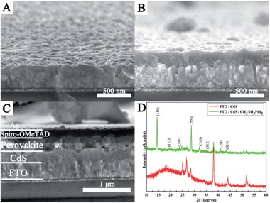 | ||
| Fig. 2 Cross-sectional FESEM images of (A) bare FTO, (B) the as-prepared CdS film and (C) the FTO/CdS/CH3NH3PbI3/HTM/Ag device. (D) XRD patterns of the CdS thin film with CH3NH3PbI3 deposition. | ||
It is well known that the role of ESLs in PSCs is to prevent the direct contact of the holes formed in the perovskite or HTM layer with the FTO electrode.34 Thus, a compact and pinhole-free surface morphology of the ESL is desirable to fabricate a high performance device. In this study, the homogeneous precipitation method is employed for the deposition of CdS thin films on FTO substrates in urea aqueous solution. The effects of different concentrations of urea from 0.5 M to 2.5 M on the morphological properties of the CdS thin film are studied. Fig. 3 shows the surface morphology of various CdS layers deposited using different concentrations of urea. As shown in Fig. 3, it is clear that urea can significantly affect the surface morphology and uniformity of the CdS thin film. The surface homogeneity of the CdS thin film increases with the increase of urea, and then decreases at higher urea concentrations. An obvious change can also be found that the grain size of CdS nanoparticles decreased as the concentration of urea increased from 0.5 to 2.5 M. This can be attributed to the grain refinement effects of urea. A similar phenomenon has been observed by other groups.35 From the above-mentioned morphological studies, it may be suggested that the concentration of urea plays an important role in controlling the morphology of CdS thin films, forming smaller crystallites via preventing their combination with each other within a certain concentration limit. It can be seen that a suitable increase in the concentration of urea can improve the uniformity of CdS thin films. A uniform dense CdS thin film with fine grain size and excellent distribution can be obtained with appropriate addition of urea (1.5 M).
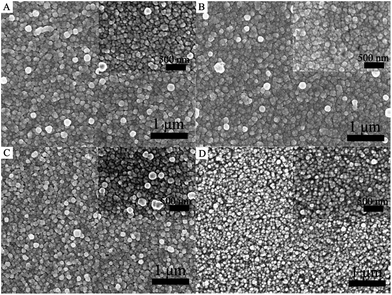 | ||
| Fig. 3 Top-view FESEM images of CdS thin films with different urea concentrations: (A) 0.5 M, (B) 1.5 M, (C) 2 M, and (D) 2.5 M. | ||
The as-synthesized CdS thin films are then used to fabricate perovskite photovoltaic devices. The difference in morphology between these samples has a direct impact on the formation of the perovskite film, as depicted in Fig. 4. As shown in Fig. 4A and B, the perovskite densely covers the entire CdS thin film. However, it should be pointed out that pinholes are clearly observed between the perovskite film and the CdS thin film, as shown in Fig. 4C and D. As depicted in Fig. 4, the formation of better contact between CdS and the perovskite layer can be related to the uniform CdS thin film, which could serve as a good scaffold for facilitating the formation of the dense crystalline perovskite layer. In contrast, the poor contact can be highly associated with the small size of CdS nanoparticles, which appears to be insufficient to guide the crystal growth of the perovskite, thus resulting in pinhole formation. Therefore, it can be established that a high quality CdS thin film is necessary to form a better contact between CdS and perovskite.
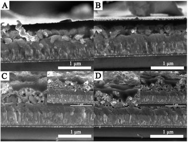 | ||
| Fig. 4 Cross-sectional FESEM images of the devices with CdS films deposited using different urea concentrations: (A) 0.5 M, (B) 1.5 M, (C) 2 M, and (D) 2.5 M. | ||
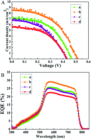
Previous reports propose that charge extraction and/or exciton dissociation occurs predominantly at the TiO2/CH3NH3PbI3 interface.36,37 Full coverage and high uniformity of the perovskite film can avoid direct contact between spiro-MeOTAD and FTO. The charge transport and collection occur along the vertical direction without the interference of any short circuit pathway, and a better PCE is ensured. In contrast, the poor contact often results in a large amount of surface defects, which leads to unsatisfactory charge extraction and severe device degradation of the resulting PSCs. As illustrated in Fig. 4, the growth of the CdS thin film has an obvious influence on the formation of a uniform perovskite layer. In this work, the as-synthesized CdS thin films using different concentrations of urea are applied as the ESL layers in the PSCs. The fabricated devices are named S1, S2, S3, and S4, respectively. The performances of PSCs according to various CdS layers are presented in Fig. 5A. The short-circuit current density (Jsc), open-circuit voltage (Voc), fill factor (FF), and PCE of the devices under AM 1.5G simulated sunlight (at 100 mW cm−2 intensity) are summarized in Table 1. S2 (Jsc = 8.51 mA cm−2, Voc = 0.52 V, FF = 51.13%) demonstrates higher conversion efficiency than other devices. This can be attributed to the dense perovskite films with a full coverage on the CdS film, forming a better contact with the CdS thin film. The better contact can reduce recombination centers and ensure a better separation and transport of photogenerated charge carriers. In contrast, S4 shows poor performance with a relatively low Jsc (5.60 mA cm−2) and FF (51.77%); in particular, the Voc is lower than that of other devices. The low PCE is attributable to the poor contact between the perovskite film and CdS thin film, which is not favorable for efficient charge separation and transfer. Therefore, the interfacial contact between the perovskite and the electron-transport material is of substantial importance. To confirm the enhancement of the photocurrent, we record the IPCE spectra, as shown in Fig. 5B. The IPCE spectrum follows the same trend as PCEs obtained for different CdS films. The IPCE spectrum shows the expected behavior for a high-performance device based on CH3NH3PbI3, and the onset of photocurrent at 800 nm is consistent with the reported bandgap of CH3NH3PbI3.38 As shown in Fig. 5B, the IPCE of S2 is remarkably higher than that of other devices in the visible region, which is mainly due to the faster electron transport process between the CdS film and the perovskite layer. Despite the fact that, among all the as-prepared devices, S2 exhibits a better efficiency, the efficiency is still rather low. The limited photovoltaic performance of the present devices could be attributed to a number of factors, and further research is needed in our next work.
| Perovskite solar cells | V oc [V] | J sc [mA cm−2] | Fill factor [%] | PCE [%] |
|---|---|---|---|---|
| S1 | 0.47 | 7.12 | 53.67 | 1.78 |
| S2 | 0.52 | 8.51 | 51.13 | 2.27 |
| S3 | 0.43 | 6.77 | 47.60 | 1.39 |
| S4 | 0.43 | 5.60 | 51.77 | 1.26 |
The insufficient stability of devices is one major concern of PSCs for their further commercialization. In our work, the photostability is further investigated by the continuous light-soaking measurement. The measurement is carried out by measuring the photocurrent generated by the cell under continuous light illumination and displaying the photocurrent density as a function of the illumination time. As illustrated in Fig. 6A, obviously, better photostability is observed for S2 during constant light illumination of 600 s, showing a slight photocurrent density decrease. S4, by contrast, exhibits an apparent decrease of photocurrent. This may be linked to the degradation of the interface between the perovskite and CdS film for S4. What's more, the air storage stability of the obtained devices is also investigated (Fig. 6B). All the devices are exposed to air for 15 days without any encapsulation (humidity 10–20%). The related parameters are listed in Table 2. The PCE of S2 declines from 2.27% to 1.56%, and S4 exhibits severe degradation. The lower performance could originate from the inferior perovskite/CdS interface, such as the one with pinholes mentioned above. Based on the discussion above, it can be concluded that a better contact is necessary to obtain high efficiency solar cells with long-term stability. Moreover, the impact of the CdS film on device stability points out a potential direction for developing appropriate electron transport materials in PSCs.
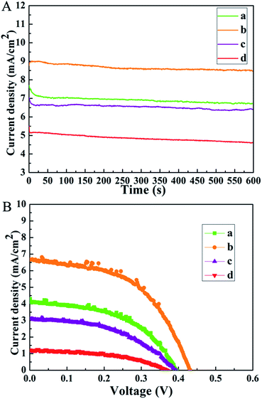 | ||
| Fig. 6 (A) Long-term photostability of (a) S1, (b) S2, (c) S3, and (d) S4, measured at a fixed bias potential of 0 V for 600 s; (B) J–V curves for (a) S1, (b) S2, (c) S3, and (d) S4. | ||
| Perovskite solar cells | V oc [V] | J sc [mA cm−2] | Fill factor [%] | PCE [%] |
|---|---|---|---|---|
| S1 | 0.40 | 4.14 | 51.97 | 0.85 |
| S2 | 0.43 | 6.66 | 54.19 | 1.56 |
| S3 | 0.39 | 3.07 | 47.24 | 0.57 |
| S4 | 0.37 | 1.20 | 47.62 | 0.21 |
4. Conclusion
In this study, we report PSCs based on CdS as the electron transport material, perovskite as the light harvester, and spiro-MeOTAD as the hole transport material. The CdS thin film is prepared by the homogeneous precipitation method in urea aqueous solution. The effects of urea concentrations on the growth of CdS thin films are studied. Then the perovskite layer is synthesized on the surface of the CdS thin film by the spin-coating method. It is found that the growth of the CdS thin film has an obvious influence on the formation of a uniform perovskite layer. Dense CdS thin films with appropriate grain sizes can ensure uniform coverage of perovskite films, forming a better contact between the CdS film and the perovskite layer, which can not only facilitate the charge transport but also reduce charge recombination at the interface of CdS/perovskite. The dependence of the photovoltaic properties of PSCs on CdS is examined carefully. The stability of PSCs is also studied. A best-performing device with a PCE of 2.27%, a Voc of 0.52 V, a Jsc of 8.51 mA cm−2, and an FF of 51.13% is demonstrated. This can be ascribed to the dense perovskite films with a full coverage on the CdS film, forming a better contact with the CdS thin film. This is effective in reducing the occurrence of trap-assisted recombination, which is favorable for charge separation at the interface and the subsequent charge transport. What's more, the best-performing device also exhibits the best stability among all the as-prepared devices. Thus, it can be concluded that the contact between CdS and the perovskite layer is the critical factor that determines the photovoltaic performance of PSCs. Moreover, the results also indicate the great potential of CdS as the electron transport material, which provides varieties for perovskite-based solar cell design.Acknowledgements
This work is financially supported by the National Natural Science Foundation of China (No. 51272086) and the Technology Development Program of Jilin Province (Grant no. 20100417).Notes and references
- A. Kojima, K. Teshima, Y. Shirai and T. Miyasaka, J. Am. Chem. Soc., 2009, 131, 6050–6051 CrossRef CAS PubMed.
- M. M. Lee, J. Teuscher, T. Miyasaka, T. N. Murakami and H. J. Snaith, Science, 2012, 338, 643–647 CrossRef CAS PubMed.
- M. Liu, M. B. Johnston and H. J. Snaith, Nature, 2013, 501, 395–398 CrossRef CAS PubMed.
- H. Zhou, Q. Chen, G. Li, S. Luo, T.-B. Song, H.-S. Duan, Z. Hong, J. You, Y. Liu and Y. Yang, Science, 2014, 345, 542–546 CrossRef CAS PubMed.
- W. S. Yang, J. H. Noh, N. J. Jeon, Y. C. Kim, S. Ryu, J. Seo and S. I. Seok, Science, 2015, 348, 1234–1237 CrossRef CAS PubMed.
- N.-G. Park, J. Phys. Chem. Lett., 2013, 4, 2423–2429 CrossRef CAS.
- H. T. Peng, W. H. Sun, Y. L. Li, W. B. Yan, P. R. Yu, H. P. Zhou, Z. Q. Bian and C. H. Huang, J. Photonics Energy, 2016, 6, 022002 CrossRef.
- Q. S. Dong, Y. T. Shi, K. Wang, Y. Li, S. F. Wang, H. Zhang, Y. J. Xing, Y. Du, X. G. Bai and T. L. Ma, J. Phys. Chem. C, 2015, 119, 10212–10217 CAS.
- Q. Wu, W. Zhou and Q. Liu, ACS Appl. Mater. Interfaces, 2016, 8, 34464–34473 CAS.
- H. J. Snaith, J. Phys. Chem. Lett., 2013, 4, 3623–3630 CrossRef CAS.
- J. H. Noh, H. I. Sang and H. H. Jin, Nano Lett., 2013, 13, 1764–1769 CrossRef CAS PubMed.
- H.-S. Kim, C.-R. Lee, J.-H. Im, K.-B. Lee, T. Moehl, A. Marchioro, S.-J. Moon, R. Humphry-Baker, J.-H. Yum and J. E. Moser, Sci. Rep., 2012, 2, 591–598 Search PubMed.
- J. H. Im, C. R. Lee and J. W. Lee, Nanoscale, 2011, 3, 4088–4093 RSC.
- N. J. Jeon, H. G. Lee and Y. C. Kim, J. Am. Chem. Soc., 2014, 136, 7837–7840 CrossRef CAS PubMed.
- A. Mei, X. Li and L. Liu, Science, 2014, 345, 295–298 CrossRef CAS PubMed.
- D. Liu and T. L. Kelly, Nat. Photonics, 2013, 8, 133–138 CrossRef.
- A. Dymshits, L. Iagher and L. Etgar, Materials, 2016, 9, 60 CrossRef.
- J. T. W. Wang, J. M. Ball and E. M. Barea, Nano lett., 2013, 14, 724–730 CrossRef PubMed.
- J. M. Ball, M. M. Lee, A. Hey and H. J. Snaith, Energy Environ. Sci., 2013, 6, 1739–1743 CAS.
- M. J. Carnie, C. Charbonneau, M. L. Davies, J. Troughton, T. M. Watson, K. Wojciechowski, H. Snaith and D. A. Worsley, Chem. Commun., 2013, 49, 7893–7895 RSC.
- Q. Zhang, C. S. Dandeneau, X. Zhou and C. Cao, Adv. Mater., 2009, 21, 4087–4108 CrossRef CAS.
- J. B. Baxter and E. S. Aydil, Appl. Phys. Lett., 2005, 86, 1–3 CrossRef.
- I. Gonzalez-Valls and M. Lira-Cantu, Energy Environ. Sci., 2009, 2, 19–34 CAS.
- L. Wang, W. F. Fu, Z. W. Gu, C. C. Fan, X. Yang, H. Y. Li and H. Z. Chen, J. Mater. Chem. C, 2014, 2, 9087–9090 RSC.
- D. –Y. Son, J. –H. Im, H. –S. Kim and N. –G. Park, J. Phys. Chem. C, 2014, 118, 16567–16573 CAS.
- M. H. Kumar, N. Yantara and S. Dharani, Chem. Commun., 2013, 49, 11089–11091 RSC.
- J. S. Jie, W. J. Zhang, Y. Jiang, X. M. Meng, Y. Q. Li and S. T. Lee, Nano Lett., 2006, 6, 1887–1892 CrossRef CAS PubMed.
- I. Hwang and K. Yong, ACS Appl. Mater. Interfaces, 2016, 8, 4226–4232 CAS.
- E. J. Juarez-Perez, M. Wuβler, F. Fabregat-Santiago, K. Lakus-Wollny, E. Mankel, T. Mayer, W. Jaegermann and I. Mora-Sero, J. Phys. Chem. Lett., 2014, 5, 680–685 CrossRef CAS PubMed.
- J. Liu, C. Gao, L. Z. Luo, Q. Y. Ye, X. L. He, L. Q. Ouyang, X. W. Guo, D. Zhuang, C. Liao, J. Mei and W. Lau, J. Mater. Chem. A, 2015, 3, 11750–11755 CAS.
- Z. W. Gu, F. Chen, X. Q. Zhang, Y. J. Liu, C. C. Fan, G. Wu, H. Y. Li and H. Z. Chen, Sol. Energy Mater. Sol. Cells, 2015, 140, 396–404 CrossRef CAS.
- J. Burschka, N. Pellet, S.-J. Moon, R. Humphry-Baker, P. Gao, M. K. Nazeeruddin and M. Grätzel, Nature, 2013, 499, 316–319 CrossRef CAS PubMed.
- A. Abate, T. Leijtens, S. Pathak, J. Teuscher, R. Avolio, M. E. Errico, J. Kirkpatrik, J. M. Ball, P. Docampo, I. McPherson and H. J. Snaith, Phys. Chem. Chem. Phys., 2013, 15, 2572–2579 RSC.
- S. Hong, A. Han, E. C. Lee, K.-W. Ko, J.-H. Park, H.-J. Song, M.-H. Han and C.-H. Han, Curr. Appl. Phys., 2015, 15, 574–579 CrossRef.
- Z. X. Zeng, L. P. Wang, A. Liang, L. Chen and J. Y. Zhang, Mater. Lett., 2007, 61, 4107–4109 CrossRef CAS.
- J. H. Heo, S. H. Im and J. H. Noh, Nat. Photonics, 2013, 7, 486–491 CrossRef CAS.
- W. Wang, H. Zheng and Y. Liu, J. Nanosci. Nanotechnol., 2016, 16, 12768–12772 CrossRef CAS.
- T. Baikie, Y. Fang and J. M. Kadro, J. Mater. Chem. A, 2013, 1, 5628–5641 CAS.
| This journal is © The Royal Society of Chemistry 2017 |

