Highly efficient and stable perovskite solar cell prepared from an in situ pre-wetted PbI2 nano-sheet array film
Xuhui
Zhang
ab,
Zhaoqian
Li
a,
Yong
Ding
c,
Linhua
Hu
a,
Jiajiu
Ye
ab,
Xu
Pan
 *a and
Songyuan
Dai
*c
aKey Laboratory of Novel Thin-Film Solar Cells, Institute of Applied Technology, Chinese Academy of Sciences, Hefei 230088, China. E-mail: xpan@rntek.cas.cn
bUniversity of Science and Technology of China, Hefei 230026, China
cState Key Laboratory of Alternate Electrical Power System with Renewable Energy Sources, North China Electric Power University, Beijing 102206, China. E-mail: sydai@ncepu.edu.cn
First published on 10th March 2017
Abstract
Due to its good pore-filling and morphology control, a two-step deposition technique has been widely used in perovskite film preparation. However, the initial PbI2 film used for the two-step deposition method is usually dense, crystalline and layered, leading to a poor quality perovskite film with a certain amount of PbI2 residue, thus resulting in an inferior stability and low power conversion efficiency (PCE) of the device. In this work, we developed an in situ pre-wetted PbI2 nano-sheet array film to achieve high-quality CH3NH3PbI3 (MAPbI3) perovskite films via a two-step deposition method. By introducing a small amount of hydrogen chloride isopropanol solution (IPA HCl) into the PbI2 precursor solution, an in situ pre-wetted PbI2 nano-sheet array film was obtained, and then a smooth, continuous, uniform, dense, and PbI2-free perovskite film was formed through a reaction with CH3NH3I. After optimization, the device prepared using the in situ pre-wetted PbI2 nano-sheet array film achieved a promising PCE of 19.19%. Moreover, it also had good reproducibility and long term stability, as the devices based on the in situ pre-wetted PbI2 nano-sheet array film retained over 80% of the initial PCE after exposing to ambient air for two months.
1. Introduction
Since the first groundbreaking report by Miyasaka in 2009,1 perovskite solar cells (PSCs) have attracted great scientific and technological interest due to their excellent performance and simple production.2–5 Over the past 7 years, the certified power conversion efficiency (PCE) of PSCs has increased from 3.8% to 22.1%.1,6–12 The impressive photovoltaic performance can be attributed to the material’s intriguing optoelectronic properties, such as a relative suitable bandgap, high charge carrier mobility, long carrier diffusion length, and high absorption coefficient and lifetime.13–17As one of the most classic organic–inorganic hybrid perovskite materials, CH3NH3PbI3 (MAPbI3) has been frequently used as a light absorber in the PSCs. The film quality of the MAPbI3 absorber is very crucial to the photovoltaic performance of the PSCs.18 Currently, various processes have been developed to improve the crystallinity, uniformity, coverage, and morphology of the MAPbI3 layer, such as a one-step approach,19–21 two-step approach,22–24 vapor approach8,25 and vapor-assisted solution approach.26,27 The two-step approach for MAPbI3 perovskite preparation was initially adapted by Michael Grätzel and his colleagues to fabricate mesoscopic PSCs,22 in which a PbI2 film was first coated on the substrate and then reacted with CH3NH3I (MAI). However, PbI2 from the initial dimethyl formamide (DMF) solution would form a dense crystalline and layered film on the substrate,28,29 which makes the conversion of PbI2 harder and results in a poor morphology of the MAPbI3 film, leading to two main problems.30,31 Firstly, an uncontrollable surface morphology and crystal size of MAPbI3 are unconducive to the improvement of the PCE and reproducibility of the PSCs. Secondly, the residual PbI2 in the MAPbI3 films also has a negative impact on the reproducibility and stability of the devices. Various methods have been developed to improve the quality of the PbI2 precursor films, such as adding additives (4-tert-butylpyridine, CH3NH3I, H2O or hydrochloric acid) into the PbI2 precursor solution,30,32–34 careful thermal or gas-quenching treatment,35,36 synthesizing nanoporous PbI2,37 and using a mixed solvent or mixed PbI2 and PbCl2 precursor solution.29,38 By means of all these methods, the crystallinity of the PbI2 layer was decreased and an adjustable morphology was obtained, which could ensure better conversion from PbI2 to MAPbI3, and precise control of the final morphology of the MAPbI3 films, so the PCE and other performances, such as stability and consistency, were enhanced.
Herein, we developed an in situ pre-wetted PbI2 nano-sheet array film (HP-PbI2) to achieve high-quality CH3NH3PbI3 (MAPbI3) perovskite films via a two-step deposition method. By introducing a small amount of hydrogen chloride isopropanol solution (IPA HCl) into the PbI2 precursor solution, an in situ pre-wetted PbI2 nano-sheet array film was obtained. This novel porous PbI2 nano-sheet array film could accelerate the reaction between PbI2 and MAI, so then a smooth, continuous, uniform, dense and PbI2-free MAPbI3 film could be prepared. Compared to the devices prepared from the conventional PbI2 film, the PCE was enhanced from 12.89% to 19.19% under an optimum addition amount of IPA HCl. Furthermore, the stability and consistency of the devices were also improved significantly.
2. Experimental
2.1 Materials and reagents
Fluorine-doped SnO2-coated transparent conducting glass (FTO, 15 Ω per square) was obtained from Pilkington TEC. CH3NH3I (MAI, 99%) and 2,2′,7,7′-tetrakis(N,N-di-p-methoxyphenylamine)-9,9-spirobifluorene (spiro-OMeTAD) were purchased from Xi’an Polymer Light Technology Corp. Titanium isopropoxide (98%), lithium bis(trifluoromethylsulphonyl) imide (Li-TFSI, 99.99%) and 4-tert-butylpyridine (TBP, 96%) were bought from Aldrich. Bis(acetylacetonate) (99%), isopropanol (IPA, 99.7%), N,N-dimethylformamide (DMF, 99.9%) and hydrogen chloride isopropanol solution (IPA HCl, for GC, ∼1.25 M (T)) were purchased from J&K Chemicals. TiO2 (particle size: about 30 nm, crystalline phase: anatase) was obtained from Dysol. Lead(II) iodide (PbI2, 99.999%) was purchased from TCI. All chemicals were used as received without further purification.2.2 Device fabrication
A 50 nm-thick TiO2 compact blocking layer (c-TiO2) was deposited on the clean and etched FTO substrate by aerosol spray pyrolysis at 450 °C, using a precursor solution of 0.4 mL of bis(acetylacetonate) and 0.6 mL of titanium diisopropoxide in 7 mL of isopropanol. A mesoporous TiO2 layer (100–150 nm in thickness) was then deposited on the c-TiO2/FTO substrate by spin coating at 5000 rpm for 30 s. After drying at 100 °C, the mesoporous TiO2 film was annealed at 510 °C for 20 min to remove the organic residue. For depositing the MAPbI3 perovskite layer, first a layer of PbI2 was spin-coated on top of the mesoporous TiO2 layer from a 1.0 M PbI2 DMF precursor solution (with or without an IPA HCl additive) at 2500 rpm for 30 s, then a 45 mg mL−1 MAI IPA solution was spin coated on the PbI2 film at 2500 rpm for 30 s immediately. The deposited film was then annealed at 105 °C for 60 min to form the perovskite layer. The HTM layer was deposited onto the perovskite layer by spin-coating at 2500 rpm for 20 s, using a solution of spiro-MeOTAD, 4-tert-butylpyridine, and lithium bis(trifluoromethylsulphonyl) imide and the Co(III)-complex. Finally, a 60–80 nm-thick Au counterelectrode was deposited by thermal evaporation on the top of the device.2.3 Measurement and characterization
Photocurrent and voltage curves (J–V) were measured with a solar simulator equipped with a 450 W xenon lamp (AAA simulator, Oriel USA) and a Keithley 2400 source meter. The light intensity was adjusted with an NREL-calibrated Si solar cell with a KG-2 filter for approximating 1 sun light intensity (100 mW cm−2). While measuring the current and voltage, the cell was covered with a black mask to define the active area of the device, and in this case it was 0.09 cm2. The incident monochromatic photon-to-current conversion efficiency (IPCE) was measured using an IPCE measuring system (Newport Corporation, CA) equipped with a Xe lamp as the light source. Time-resolved photoluminescence (TR-PL) spectra were collected using a transient state spectrophotometer (F900, Edinburgh Instruments). The samples were excited with a 660 nm pulsed diode laser with a repetition rate of 2.5 MHz and an excitation intensity of about 14 nJ cm−2. Steady-state fluorescence (PL) spectra were recorded by exciting the perovskite films without or with a TiO2 layer at 473 nm with a standard 450 W xenon CW lamp. The signals were recorded using a spectrofluorometer (Photon Technology International) and analyzed using the software Fluorescence. The morphologies of the PbI2 and CH3NH3PbI3 (MAPbI3) films were characterized using a field-emission scanning electron microscope (FE-SEM, ZEISS ΣIGMA) and atomic force microscopy (AFM, using a MultiMode V (Veeco) viewer and analyzer). The X-ray diffraction spectra of the PbI2 and MAPbI3 films were recorded on an X’pert PRO X-ray diffractometer. The data were collected at room temperature in the 2θ range 10–60°. Ultraviolet-visible (UV-vis) absorption spectra of all samples were measured using an UV-vis spectrophotometer (U-3900H, HITACHI, Japan) at room temperature.3. Results and discussion
Scheme 1 shows the preparation process of the perovskite films from (a) the conventional PbI2 film (C-PbI2) and (b) the PbI2 film fabricated using IPA HCl as the additive in the precursor PbI2 DMF solution (HP-PbI2). For the conventional PbI2 film preparation, generally, PbI2 is dissolved in pure DMF, and this precursor solution is deposited on the substrate to fabricate the PbI2 film by spin-coating. Although DMF has a good solubility for PbI2, it is highly volatile, resulting in an inhomogeneous, layered, fast crystallized, and dense PbI2 film. Then a nonuniform perovskite film with an amount of PbI2 residue will be obtained because of the limited diffusivity of MAI and the PbI2 film cannot be transformed completely in a short time. By introducing a suitable amount of IPA HCl into the PbI2 DMF precursor solution, the quality of the initial PbI2 film was significantly improved. IPA is uniformly distributed in the PbI2 film, and could provide reaction channels for the reaction of PbI2 and MAI. Meanwhile, the existence of HCl broke the continuous PbI2 crystals in the PbI2 film into PbI2 nano-sheet arrays, leading to a complete and homogeneous reaction between PbI2 and MAI. The optimized amount of IPA HCl for PbI2 film preparation is 100 μL of IPA HCl in 1 mL of PbI2 DMF precursor solution.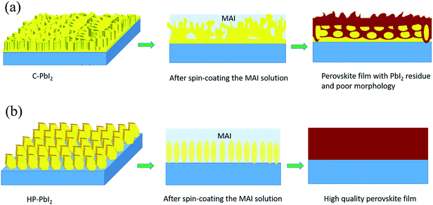 | ||
| Scheme 1 Schematic diagrams of the deposition of the perovskite films for (a) C-PbI2 and (b) HP-PbI2. | ||
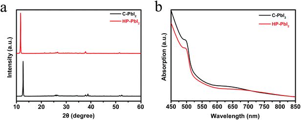
We studied the surface morphologies of C-PbI2 and HP-PbI2 using scanning electron microscopy (SEM). As shown in Fig. 1a and b, the conventional PbI2 DMF precursor solution formed a dense, inhomogeneous, layered PbI2 film (C-PbI2). Due to the addition of IPA HCl, HP-PbI2 was homogeneous and porous, and the continuous PbI2 crystals were broken into PbI2 nano-sheet arrays (Fig. 1c and d). This may be due to the existence of HCl in the PbI2 precursor solution, which led to the formation of the PbI2·HCl coordination complexes. Fig. 1e shows the AFM images of HP-PbI2, with a very rough surface being observed. Owing to the formation of the PbI2 nano-sheet arrays, the HP-PbI2 film had a high surface roughness, which is in accordance with the SEM data. The XRD pattern of HP-PbI2 exhibited a very strong unknown XRD peak at around 11.6° as shown in Fig. 2a, with a clear shift from the main peak of PbI2 for C-PbI2. This result also suggested that the addition of IPA HCl may have led to the formation of a novel PbI2·xHCl precursor. The UV-vis absorption spectra of C-PbI2 and HP-PbI2 are shown in Fig. 2b. Compared with C-PbI2, the absorption of HP-PbI2 was a little weaker. As the continuous PbI2 crystals in HP-PbI2 were broken into PbI2 nano-sheet arrays, this led to HP-PbI2 being more porous than C-PbI2. Then less light would be absorbed by HP-PbI2, so the absorption was weaker.
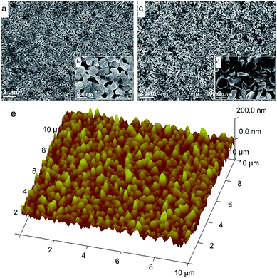 | ||
| Fig. 1 Top-view SEM images of (a and b) C-PbI2 and (c and d) HP-PbI2, and (e) AFM image (10 μm × 10 μm) of HP-PbI2. | ||
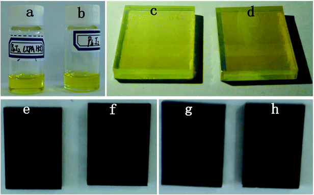
As can been seen from Fig. 3a and b, there was almost no obvious difference in the colour between the PbI2 DMF solution with IPA HCl additive and without IPA HCl additive. After the PbI2 films (HP-PbI2 and C-PbI2) had been prepared from these solutions, the colour of HP-PbI2 was a little lighter than the colour of C-PbI2. As HP-PbI2 was more porous than C-PbI2, less light would be absorbed, so the colour of HP-PbI2 was lighter. This result was in agreement with the absorption spectra of HP-PbI2 and C-PbI2 (Fig. 2b). After spin-coating the MAI IPA solution on HP-PbI2 and C-PbI2, the HP-PbI2/MAI film changed to dark brown immediately, while the C-PbI2/MAI film only turned to pale brown (Fig. 3e and f), indicating that the existence of IPA in the PbI2 film can accelerate the reaction between the PbI2 layer and MAI layer. By annealing at 105 °C for 60 min, the films of HP-PbI2/MAI and HP-PbI2/MAI converted into perovskite films and the HCl in HP-PbI2 was released to the air.34,39 The real images of the perovskite films prepared from HP-PbI2 and C-PbI2 are shown in Fig. 3g and h. From the real images, we can see that the perovskite film prepared from HP-PbI2 was more uniform and smoother than the film prepared from C-PbI2.
Fig. 4 shows the top SEM images of the perovskite films prepared from C-PbI2 and HP-PbI2. Compared to the MAPbI3 perovskite film prepared from C-PbI2, the top morphology of the MAPbI3 perovskite film prepared from HP-PbI2 is markedly changed. From Fig. 4a and b, for the surface morphology of the MAPbI3 perovskite film fabricated by C-PbI2, huge amounts of uneven grains are observed. Moreover, the whole MAPbI3 film was also very nonuniform with many voids and pinholes. For the MAPbI3 perovskite film prepared by HP-PbI2, a uniform, dense and homogeneous film was obtained (Fig. 4c and d). This change can be ascribed to the following reason. The MAI droplet will react with the PbI2 grains quickly when it comes into contact with the surface of the PbI2 film. For C-PbI2, it was dense and crystallized quickly, so the perovskite ripening process only occurs on the surface of the PbI2 film and at the periphery of the PbI2 grains. Moreover, during the perovskite ripening process, great volume expansion occurred for the material because the density of the MAPbI3 film was only 4.29 g cm−3 while that of the PbI2 film was 6.16 g cm−3.40,41 As C-PbI2 was too dense, there was no space for horizontal volume expansion during the perovskite ripening process. Therefore, the volume expansion mostly occurred in the vertical direction of the PbI2 film. Hence, there were huge amounts of uneven grains on the MAPbI3 film prepared from C-PbI2. In contrast, for HP-PbI2, it was homogeneous, porous and in situ pre-wetted by IPA, so could be infiltrated by MAI sufficiently. After annealing, a high quality MAPbI3 perovskite film was formed. For the mesoscopic PSCs, a poor quality perovskite film results in poor light absorption and increases the charge recombination, so the MAPbI3 film prepared from HP-PbI2 is more suitable for the fabrication of high performance PSCs.
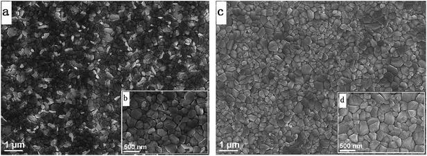 | ||
| Fig. 4 Top-view SEM images of (a and b) the perovskite film prepared from C-PbI2 and (c and d) the perovskite film prepared from HP-PbI2. | ||
Fig. 5a shows the XRD patterns of the perovskite films prepared from C-PbI2 and HP-PbI2. A strong diffraction peak of PbI2 around 12.6° is observed in the XRD pattern of the MAPbI3 film prepared from C-PbI2, indicating incomplete conversion of PbI2 in MAPbI3 preparation, while for the MAPbI3 film prepared from HP-PbI2, the signal of PbI2 almost disappears. Since C-PbI2 was too dense and crystallized quickly, it was hard for MAI to permeate to the interior and bottom of the PbI2 film. Therefore, the perovskite ripening process only occurs on the top of the PbI2 film and periphery of the PbI2 grains. Hence, a certain amount of PbI2 residue existed in the MAPbI3 film based on C-PbI2. For HP-PbI2, two great improvements can help to eliminate the PbI2 residue effectively. Because IPA has a good affinity to PbI2, it can infiltrate into the PbI2 film sufficiently and homogeneously. After spin-coating the MAI IPA solution, a concentration gradient of MAI between the MAI layer and PbI2 layer was formed. Through the IPA diffusion channels, MAI could diffuse to the interior and bottom of the PbI2 film rapidly. Good permeation of MAI in the PbI2 film was propitious for the reaction of PbI2 and MAI. Moreover, the ordered PbI2 nano-sheet arrays also can react with MAI efficiently. Therefore, compared to C-PbI2, HP-PbI2 can eliminate the PbI2 residue effectively in the MAPbI3 perovskite preparation. The UV-vis absorption spectra of the perovskite films based on C-PbI2 and HP-PbI2 are shown in Fig. 5b. There was a very notable increase in the absorption of the perovskite film prepared from HP-PbI2 between 500–780 nm, while the perovskite film prepared from C-PbI2 had a relatively poor absorption. These results also demonstrated that HP-PbI2 was beneficial for the full conversion of PbI2 to MAPbI3 perovskite.
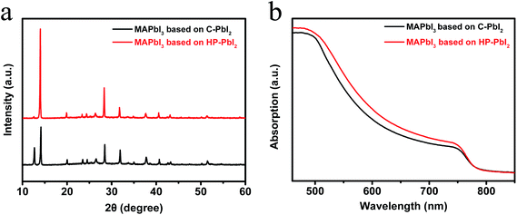 | ||
| Fig. 5 (a) XRD patterns and (b) UV-vis absorption spectra of the perovskite films prepared from C-PbI2 and HP-PbI2. | ||
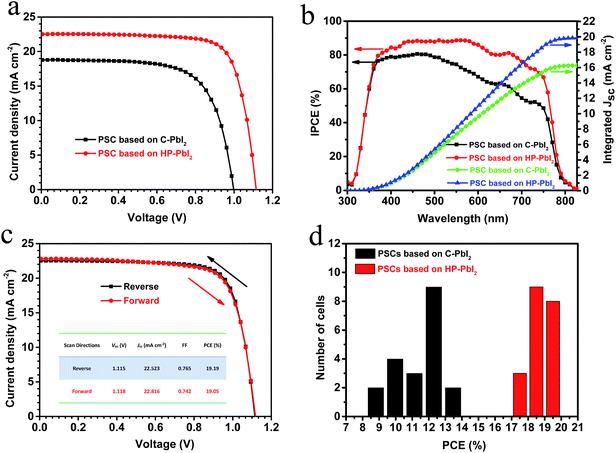
Using the perovskite films based on C-PbI2 and HP-PbI2 as photoactive layers, we fabricated mesoscopic PSCs with a structure of FTO/compact TiO2/porous TiO2/MAPbI3/spiro-MeOTAD/Au. The current–voltage (J–V) curves of typical PSCs based on C-PbI2 and HP-PbI2 are presented in Fig. 6a and the corresponding detailed parameters are summarized in Table 1. The typical device based on C-PbI2 exhibited a PCE of 12.89%, open-circuit voltage (Voc) of 1.00 V, short-circuit current (Jsc) of 18.79 mA cm−2, and fill factor (FF) of 0.68. When the perovskite layer was prepared from HP-PbI2 during the device fabrication, the resulting device exhibited better performance, with Voc increasing from 1.00 to 1.12 V, Jsc increasing from 18.89 to 22.52 mA cm−2, and the FF increasing from 0.68 to 0.77. Consequently, the PCE improved from 12.89% to 19.19%. The enhanced Voc and FF can be explained by the reduced charge carrier recombination which is due to the high quality of the MAPbI3 film with fewer defects and trap sites when prepared from HP-PbI2. Moreover, as the MAPbI3 film based on HP-PbI2 was of high quality, the hysteresis of the device would be suppressed, which agreed with the J–V curves of the typical PSC based on HP-PbI2 measured in different scan directions (Fig. 6c). Owing to the full conversion of PbI2 to CH3NH3PbI3 and as the MAIPbI3 film was highly crystalline, more visible light would be absorbed and converted, so the Jsc of the PSC based on HP-PbI2 increased obviously. The incident photon-to-current conversion efficiency (IPCE) spectra for the typical PSCs based on C-PbI2 and HP-PbI2 are shown in Fig. 6b. The PSC based on HP-PbI2 showed a much higher IPCE than the PSC based on C-PbI2, especially at long wavelengths. The integrated currents of the PSC based on HP-PbI2 and C-PbI2 are 19.95 and 16.37 mA cm−2, which are close to the measured values from the J–V curves. Statistical PCE distributions of 20 samples of the PSCs based on C-PbI2 and HP-PbI2 fabricated in one experiment are shown in Fig. 6d. The PSCs based on HP-PbI2 showed a narrower PCE distribution than the PSCs based on C-PbI2, which meant a higher consistency was obtained by the PSCs based on HP-PbI2.
| Samples | V oc (V) | J sc (mA cm−2) | FF | PCE (%) |
|---|---|---|---|---|
| PSC based on C-PbI2 | 1.00 | 18.79 | 0.68 | 12.89 |
| PSC based on HP-PbI2 | 1.12 | 22.52 | 0.77 | 19.19 |
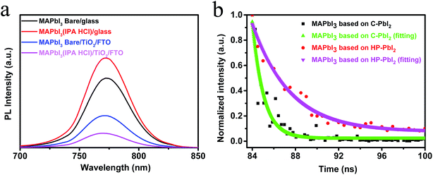
Generally, for high efficiency devices, effective charge transport, low charge recombination and long carrier lifetime are needed. A high quality perovskite film may play a key role in achieving these factors for the PSCs. To further study the quality of the perovskite films based on C-PbI2 and HP-PbI2 and the electron transport process in the devices, we investigated the steady-state photoluminescence (PL) spectra for the two kinds of perovskite films on different substrates under the excitation wavelength of 473 nm. The PL spectra of glass/MAPbI3(Bare), glass/MAPbI3(IPA HCl), glass/TiO2/MAPbI3(Bare) and glass/TiO2/MAPbI3(IPA HCl) films are shown in Fig. 7a. The MAPbI3(Bare) and MAPbI3(IPA HCl) films represent the perovskite films that were prepared from C-PbI2 and HP-PbI2, respectively. In comparison to the sample of glass/MAPbI3(Bare), glass/MAPbI3(IPA HCl) presented a higher PL intensity. After adding the TiO2 layer between the perovskite layer and glass, great quenching effects occurred for both of the samples glass/TiO2/MAPbI3(Bare) and glass/TiO2/MAPbI3(IPA HCl). Moreover, glass/TiO2/MAPbI3(IPA HCl) had a lower intensity. These results suggested that the electrons in the MAPbI3 films prepared from HP-PbI2 could enter into the TiO2 electron transport layer easily. In other words, the MAPbI3 films prepared from HP-PbI2 were of high quality with fewer defects and trap sites, which were conducive to electron diffusion to the electron transport layer. Time-resolved PL decay (TR-PL) curves of the perovskite films based on C-PbI2 and HP-PbI2 are shown in Fig. 7b. The MAPbI3 perovskite films were prepared on glass. From the TR-PL curves, the charge transfer and carrier recombination behavior in the perovskite films were estimated. From Fig. 7b, the carrier lifetime of the MAPbI3 film prepared from HP-PbI2 was 3.8 ns, which was much longer than that of the MAPbI3 film prepared from C-PbI2 (1.1 ns). A high quality MAPbI3 perovskite film with fewer defects and trap sites was obtained from HP-PbI2, so the carrier lifetime was increased. This result was in accordance with the PL spectra. Hence, the efficiency of the PSCs based on HP-PbI2 was enhanced.
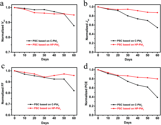
In addition, the stability of the PSCs based on C-PbI2 and HP-PbI2 was investigated. All cells were unsealed and tested in ambient air at room temperature and with a humidity of 30–75%. The Voc, Jsc, FF, and PCE stability curves of the PSCs based on C-PbI2 and HP-PbI2 are shown in Fig. 8. After espousing in ambient air for two months, over 80% of the initial PCE was retained by the PSC based on HP-PbI2, while the PCE of the PSC based on C-PbI2 dropped to 40%. Obviously, the PSC based on HP-PbI2 showed very good long-term stability. According to the literature,30,42 the unreacted PbI2 in the MAPbI3 perovskite film plays a negative role in the long-term stability of the devices. In comparison with the perovskite film prepared from C-PbI2 which had a large amount of PbI2 residue, the perovskite film prepared from HP-PbI2 was PbI2-free. Moreover, as the perovskite film prepared from HP-PbI2 was denser and had a higher crystallinity, the harmful substances in the air for perovskites, such as moisture, were less able to penetrate into the internal perovskite layer, so the perovskite film did not decompose easily. Therefore, the PSC based on HP-PbI2 was more stable than the PSC based on C-PbI2 in the ambient air.
4. Conclusion
In summary, we have developed an in situ pre-wetted PbI2 nano-sheet array film to achieve high-quality CH3NH3PbI3 (MAPbI3) perovskite films via a two-step deposition method. By introducing a small amount of IPA HCl into the PbI2 precursor solutions, an in situ pre-wetted PbI2 nano-sheet array film was obtained. Both the HCl and IPA in the IPA HCl solution have a positive impact on the formation of the perovskite film. Through the IPA diffusion channels in the PbI2 film, MAI could diffuse to the interior and bottom of the PbI2 film rapidly. Meanwhile, the existence of HCl broke the continuous PbI2 crystals in the PbI2 film into PbI2 nano-sheet arrays. The breaking of the ordered PbI2 crystal structure and good permeation of MAI in the PbI2 film can make the reaction between PbI2 and MAI proceed completely and homogeneously. After reacting with MAI, a smooth, continuous, uniform, dense, and PbI2-free perovskite film was formed. The influence of the addition of IPA HCl on the formation rate, morphology, chemical composition, crystallization, absorbance, and carrier transportation properties of the perovskite films was systemically investigated. With the optimized amount of IPA HCl, which was 100 μL of IPA HCl added in 1 mL of PbI2 DMF precursor solution, a promising PCE of 19.19% was achieved with the photovoltaic performance giving a Voc of 1.12 V, Jsc of 22.52 mA cm−2 and FF of 0.77, which was much higher than the devices prepared from the conventional PbI2 film. Additionally, the devices fabricated using in situ pre-wetted PbI2 nano-sheet array films showed very good long-term stability in ambient air due to their PbI2-free and high quality perovskite film. It is expected that our work provides a simple and rapid way to prepare stable and high efficiency PSCs.Acknowledgements
This work was financially supported by the National High Technology Research and Development Program of China under Grant No. 2015AA050602, the National Natural Science Foundation of China under Grant No. 21273242, and State Key Laboratory of Alternate Electrical Power System with Renewable Energy Sources under Grant No. LAPS14012. This work was also supported by the Science and Technology Support Program of Jiangsu Province under Grant No. BE2014147-4 and the External Cooperation Program of BIC, Chinese Academy of Sciences under Grant No. GJHZ1607.References
- A. Kojima, K. Teshima, Y. Shirai and T. Miyasaka, J. Am. Chem. Soc., 2009, 131, 6050–6051 CrossRef CAS PubMed.
- N. G. Park, Mater. Today, 2015, 18, 65–72 CrossRef CAS.
- M. Grätzel, Nat. Mater., 2014, 13, 838–842 CrossRef PubMed.
- H. Snaith and L. Schmidt-Mende, APL Mater., 2014, 2, 081201 CrossRef.
- T. A. Berhe, W. N. Su, C. H. Chen, C. J. Pan, J. H. Cheng, H. M. Chen, M. C. Tsai, L. Y. Chen, A. A. Dubale and B. J. Hwang, Energy Environ. Sci., 2016, 9, 323–356 CAS.
- H. S. Kim, C. R. Lee, J. H. Im, K. B. Lee, T. Moehl, A. Marchioro, S. J. Moon, R. H. Baker, J. H. Yum, J. E. Moser, M. Grätzel and N. G. Park, Sci. Rep., 2012, 2, 591 Search PubMed.
- J. M. Ball, M. M. Lee, A. Hey and H. J. Snaith, Energy Environ. Sci., 2013, 6, 1739–1743 CAS.
- M. Liu, M. B. Johnston and H. J. Snaith, Nature, 2013, 501, 395–398 CrossRef CAS PubMed.
- N. J. Jeon, J. H. Noh, Y. C. Kim, W. S. Yang, S. Ryu and S. I. Seok, Nat. Mater., 2014, 13, 897–903 CrossRef CAS PubMed.
- H. P. Zhou, Q. Chen, G. Li, S. Luo, T. B. Song, H. S. Duan, Z. R. Hong, J. B. You, Y. S. Liu and Y. Yang, Science, 2014, 345, 542–546 CrossRef CAS PubMed.
- W. S. Yang, J. H. Noh, N. J. Jeon, Y. C. Kim, S. Ryu, J. Seo and S. I. Seok, Science, 2015, 348, 1234–1237 CrossRef CAS PubMed.
- The National Renewable Energy Laboratory (NREL), 2017, http://www.nrel.gov/ncpv/images/efficiency_chart.jpg.
- A. Sharenko and M. F. Toney, J. Am. Chem. Soc., 2015, 138, 463–470 CrossRef PubMed.
- G. Xing, N. Mathews, S. Sun, S. S. Lim, Y. M. Lam, M. Grätzel, S. Mhaisalkar and T. C. Sum, Science, 2013, 342, 344–347 CrossRef CAS PubMed.
- H. J. Snaith, J. Phys. Chem. Lett., 2013, 4, 3623–3630 CrossRef CAS.
- X. Zhang, J. Ye, L. Zhu, H. Zheng, G. Liu, X. Liu, B. Duan, X. Pan and S. Dai, Nanoscale, 2017, 9, 4691–4699 RSC.
- T. Salim, S. Sun, Y. Abe, A. Krishna, A. C. Grimsdale and Y. M. Lam, J. Mater. Chem. A, 2015, 3, 8943–8969 CAS.
- Q. Guo, C. Li, W. Qiao, S. Ma, F. Wang, B. Zhang, L. Hu, S. Dai and Z. Tan, Energy Environ. Sci., 2016, 9, 1486–1494 CAS.
- K. Wojciechowski, M. Saliba, T. Leijtens, A. Abate and H. J. Snaith, Energy Environ. Sci., 2014, 7, 1142–1147 CAS.
- D. P. McMeekin, G. Sadoughi, W. Rehman, G. E. Eperon, M. Saliba, M. T. Horantner, A. Haghighirad, N. Sakai, L. Korte, B. Rech, M. B. Johnston, L. M. Herz and H. J. Snaith, Science, 2016, 351, 151–155 CrossRef CAS PubMed.
- D. Bi, W. Tress, M. I. Dar, P. Gao, J. Luo, C. Renevier, K. Schenk, A. Abate, F. Giordano, J. C. Baena, J. Decoppet, S. M. Zakeeruddin, M. K. Nazeeruddin, M. Grätzel and A. Hagfeldt, Sci. Adv., 2016, 2, e1501170 Search PubMed.
- J. Burschka, N. Pellet, S.-J. Moon, R. Humphry-Baker, P. Gao, M. K. Nazeeruddin and M. Grätzel, Nature, 2013, 499, 316–319 CrossRef CAS PubMed.
- X. Zhang, J. Ye, L. Zhu, H. Zheng, X. Liu, X. Pan and S. Dai, ACS Appl. Mater. Interfaces, 2016, 8, 35440–35446 CAS.
- Z. G. Xiao, C. Bi, Y. C. Shao, Q. F. Dong, Q. Wang, Y. B. Yuan, C. G. Wang, Y. L. Gao and J. S. Huang, Energy Environ. Sci., 2014, 7, 2619–2623 CAS.
- O. Malinkiewicz, A. Yella, Y. H. Lee, G. M. Espallargas, M. Graetzel, M. K. Nazeeruddin and H. J. Bolink, Nat. Photonics, 2014, 8, 128–132 CrossRef CAS.
- Q. Chen, H. Zhou, Z. Hong, S. Luo, H. Duan, H. Wang, Y. Liu, G. Li and Y. Yang, J. Am. Chem. Soc., 2013, 136, 622–625 CrossRef PubMed.
- C. Li, F. Z. Wang, J. Xu, J. X. Yao, B. Zhang, C. F. Zhang, M. Xiao, S. Y. Dai, Y. F. Li and Z. A. Tan, Nanoscale, 2015, 7, 9771–9778 RSC.
- D. Bi, A. M. El-Zohry, A. Hagfeldt and G. Boschloo, ACS Photonics, 2015, 2, 589–594 CrossRef CAS.
- Y. Wu, A. Islam, X. Yang, C. Qin, J. Liu, K. Zhang, W. Peng and L. Han, Energy Environ. Sci., 2014, 7, 2934–2938 CAS.
- H. Zhang, J. Mao, H. X. He, D. Zhang, H. L. Zhu, F. X. Xie, K. S. Wong, M. Grätzel and W. C. H. Choy, Adv. Energy Mater., 2015, 5, 1501354 CrossRef.
- F. Li, C. Bao, W. Zhu, B. Lv, W. Tu, T. Yu, J. Yang, X. Zhou, Y. Wang, X. Wang, Y. Zhou and Z. Zou, J. Am. Chem. Soc., 2016, 4, 11372–11380 CAS.
- Y. Xie, F. Shao, Y. Wang, T. Xu, D. Wang and F. Huang, ACS Appl. Mater. Interfaces, 2015, 7, 12937–12942 CAS.
- C. G. Wu, C. H. Chiang, Z. L. Tseng, M. K. Nazeeruddin, A. Hagfeldt and M. Grätzel, Energy Environ. Sci., 2015, 8, 2725–2733 CAS.
- G. Li, T. Zhang and Y. Zhao, J. Mater. Chem. A, 2015, 3, 19674–19678 CAS.
- J. Cao, F. Wang, H. Yu, Y. Zhou, H. Lu, N. Zhao and C. Wong, J. Mater. Chem. A, 2016, 4, 10223–10230 CAS.
- K. Hwang, Y.-S. Jung, Y.-J. Heo, F. H. Scholes, S. E. Watkins, J. Subbiah, D. J. Jones, D.-Y. Kim and D. Vak, Adv. Mater., 2015, 27, 1241–1247 CrossRef CAS PubMed.
- Y. Zhao and K. Zhu, J. Mater. Chem. A, 2015, 3, 9086–9091 CAS.
- M. Wang, C. Shi, J. Zhang, N. Wu and C. Ying, J. Solid State Chem., 2015, 231, 20–24 CrossRef CAS.
- G. Li, T. Zhang, N. Guo, F. Xu, X. Qian and Y. Zhao, Angew. Chem., Int. Ed., 2016, 55, 13460–13464 CrossRef CAS PubMed.
- T. Baikie, Y. Fang, J. M. Kadro, M. Schreyer, F. Wei, S. G. Mhaisalkar, M. Grätzel and T. J. White, J. Mater. Chem. A, 2013, 1, 5628–5641 CAS.
- T. Zhang, M. Yang, Y. Zhao and K. Zhu, Nano Lett., 2015, 15, 3959–3963 CrossRef CAS PubMed.
- G. Niu, X. Guo and L. Wang, J. Mater. Chem. A, 2015, 3, 8970–8980 CAS.
| This journal is © The Royal Society of Chemistry 2017 |

