Anti-solvent dependent device performance in CH3NH3PbI3 solar cells: the role of intermediate phase content in the as-prepared thin films†
Yang
Li
ab,
Jianan
Wang
cd,
Yi
Yuan
*c,
Xiandui
Dong
a and
Peng
Wang
 *c
*c
aChangchun Institute of Applied Chemistry, Chinese Academy of Sciences, Changchun, 130022, China
bUniversity of Chinese Academy of Sciences, Beijing, 100049, China
cDepartment of Chemistry, Zhejiang University, Hangzhou, 310028, China. E-mail: yyuan@zju.edu.cn; pw2015@zju.edu.cn
dSchool of Materials Science and Engineering, Harbin Institute of Technology, Harbin 150001, China
First published on 20th April 2017
Abstract
For high-performance perovskite solar cells, one-step solution deposition with anti-solvent washing is reported as an excellent processing method. In this paper, we employ attenuated total reflection Fourier transform infrared spectroscopy (ATR-FTIR), to quantitatively evaluate the relative contents of an intermediate phase in the as-prepared films, altered by anti-solvents, i.e. dichloromethane (DCM), toluene (TL), and diethyl ether (DE). Based on the joint measurements of scanning electron microscopy (SEM), X-ray diffraction (XRD), photoluminescence (PL), femtosecond transient absorption (fs-TA), current–voltage (J–V), and impedance spectroscopy, we reveal that a high content of the intermediate phase endowed with the anti-solvent DE is beneficial to film quality and device efficiency. A high coverage and pin-hole free CH3NH3PbI3 film with a long PL lifetime attained via DE washing is utilized to fabricate a CH3NH3PbI3 solar cell exhibiting over 17% power conversion efficiency. It is found that the formation of a high content intermediate phase in the as-prepared thin film is crucial to finally produce a dense and compact perovskite film with the aid of thermal annealing.
Introduction
Organic–inorganic hybrid perovskite solar cells have gone through a rapid development in the past five years.1–10 Continuous efforts on solvent engineering,11–13 composition engineering,6,14–16 and interface engineering5,17–19 have led to the highest certified power conversion efficiency (PCE) of 22.1% for a small-area, single-junction perovskite solar cell.20 In a typical perovskite solar cell, a several-hundred-nanometer-thick perovskite film is sandwiched between an electron-transporting material (ETM) and a hole-transporting material (HTM). For an efficient device, the preparation of a smooth, compact, and uniform perovskite film is highly pertinent to avoid charge recombination. In this regard, various processing methods to afford high-quality perovskite films have been reported, such as one-step deposition,21–24 sequential deposition,3,25–30 and vapor deposition.4,31,32So far high-efficiency perovskite solar cells have always been made via an anti-solvent washing based one-step deposition method.6,8–10 In 2014, Jeon et al.11 demonstrated that an intermediate phase CH3NH3I–PbI2–DMSO, a Lewis acid–base adduct,33 can be formed in the as-prepared thin film with TL as an anti-solvent. The formation of the intermediate phase is crucial to slow down the rapid reaction between CH3NH3I and PbI2 in the process of spin coating. During subsequent thermal annealing intramolecular exchange between DMSO and CH3NH3I in the solid containing the intermediate phase leads to a high-quality perovskite film.7,34 Later Jung et al.35 put forward that anti-solvents featuring large dipole moments (i.e. chlorobenzene and o-dichlorobenzene) can induce a transformation directly to a crystalline perovskite phase bypassing the intermediate phase. However, the presence of an intermediate phase in the as-prepared film using chlorobenzene was still observed.8 Other anti-solvents i.e. DE,36,37 hexane,38 chloroform,39 and iodobenzene40 were also reported for the fabrication of perovskite solar cells, and the device performance varied significantly.
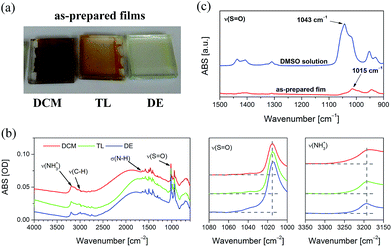
Both perovskite phase and intermediate phase are likely to coexist in the as-prepared films. Therefore, we assume that the content of an intermediate phase may have a critical influence on the subsequent crystallization of perovskite thin films. In our preliminary experiments, we also observed a remarkable difference in the colors of the as-prepared films (Fig. 1a) when DCM, TL, and DE were used as anti-solvents, suggesting different ratios of perovskite and intermediate phases. In this paper, we will scrutinize the anti-solvent dependent device performance of CH3NH3PbI3-based solar cells, by taking a close look at the impact of intermediate phase content on the morphology, crystallinity, photophysical and electrical behaviors of thin films.
Results and discussion
As detailed in the Experimental section, we first fabricated compact titania on fluorine-doped tin oxide (FTO) by a hydrothermal method, followed by the deposition of mesoporous titania and thermal doping of LiTFSI.41 Afterwards, CH3NH3PbI3 thin films were deposited on titania via one-step spin coating with the aid of anti-solvent washing. Fig. 1a compares the as-prepared films with diverse colors, which are likely associated with different ratios of perovskite to intermediate phases (CH3NH3I–PbI2–DMSO).In order to quantify the relative contents of the intermediate phase, we carried out ATR-FTIR measurements. As shown in Fig. 1b, the vibrational bands centered at 3188 ± 3 cm−1, can be assigned to NH3+ in CH3NH3I of both perovskite and intermediate phases. However, the bands peaked at 1015 cm−1 due to S![[double bond, length as m-dash]](https://www.rsc.org/images/entities/char_e001.gif) O are only from the intermediate phase. Note that the presence of the intermediate phase in these films can be identified with the bands embodying reduced S
O are only from the intermediate phase. Note that the presence of the intermediate phase in these films can be identified with the bands embodying reduced S![[double bond, length as m-dash]](https://www.rsc.org/images/entities/char_e001.gif) O bond strength, i.e. 1015 cm−1 for CH3NH3I–PbI2–DMSO versus 1043 cm−1 for pure DMSO (Fig. 1c).36 In terms of the Beer–Lambert law, the peak intensity of NH3+ is proportional to the total concentration of the perovskite and intermediate phases, while the peak intensity of S
O bond strength, i.e. 1015 cm−1 for CH3NH3I–PbI2–DMSO versus 1043 cm−1 for pure DMSO (Fig. 1c).36 In terms of the Beer–Lambert law, the peak intensity of NH3+ is proportional to the total concentration of the perovskite and intermediate phases, while the peak intensity of S![[double bond, length as m-dash]](https://www.rsc.org/images/entities/char_e001.gif) O is proportional to the concentration of the intermediate phase. Hence, the relative content of the intermediate phase could be determined via the intensity ratio of S
O is proportional to the concentration of the intermediate phase. Hence, the relative content of the intermediate phase could be determined via the intensity ratio of S![[double bond, length as m-dash]](https://www.rsc.org/images/entities/char_e001.gif) O and NH3+ peaks, as tabulated in Table 1. As listed in Table 1, the intensity ratios of S
O and NH3+ peaks, as tabulated in Table 1. As listed in Table 1, the intensity ratios of S![[double bond, length as m-dash]](https://www.rsc.org/images/entities/char_e001.gif) O and NH3+ peaks increase in the order DCM < TL < DE, indicating the increased content of the intermediate phase in the as-prepared thin films.
O and NH3+ peaks increase in the order DCM < TL < DE, indicating the increased content of the intermediate phase in the as-prepared thin films.
![[double bond, length as m-dash]](https://www.rsc.org/images/entities/char_e001.gif) O and NH3+ vibrational bands from Fig. 1b
O and NH3+ vibrational bands from Fig. 1b
| Anti-solvent | [mOD] | [mOD] | [mOD] | [mOD] | |
|---|---|---|---|---|---|
a ΔAν(NH3+) and ΔAν(S![[double bond, length as m-dash]](https://www.rsc.org/images/entities/char_e001.gif) O) were obtained via equations O) were obtained via equations  and and  . .
|
|||||
| DCM | 41 | 51 | 58 | 86 | 2.8 |
| TL | 19 | 28 | 43 | 79 | 4.0 |
| DE | 5 | 12 | 27 | 70 | 6.1 |
SEM measurements were further conducted to study the effect of anti-solvents on the morphology of CH3NH3PbI3. Fig. 2 gives the SEM images of CH3NH3PbI3 films after 10 min annealing at 100 °C. A porous film with a wide size distribution of round pinholes was obtained with DCM as the anti-solvent (Fig. 2a and b). In contrast, the TL-treated film (Fig. 2c and d) possesses numerous irregular pinholes with smaller sizes. However, a dense, compact, and pinhole-free film (Fig. 2e and f) fabricated via DE washing features a granular structure. The grain sizes are in the range from a few hundred nanometers to several micrometers. It can be concluded that the morphologies of CH3NH3PbI3 thin films are strongly influenced by anti-solvents.
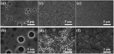 | ||
| Fig. 2 SEM images of annealed CH3NH3PbI3 thin films on titania made with different anti-solvents: (a and b) DCM, (c and d) TL, and (e and f) DE. | ||
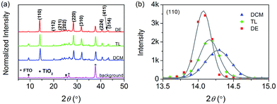
The crystallinity of CH3NH3PbI3 films on titania obtained via anti-solvent washing was also surveyed by means of XRD measurements. As depicted in Fig. 3a, the diffraction peaks are assigned to the lattice planes (110), (112), (211), (202), (220), (310), (224), and (411) respectively. The intensity ratios of the (110) to (310) diffraction peaks were calculated to be 2.0 for DE, 1.2 for TL, and 1.3 for DCM suggesting the influence of anti-solvents on crystal orientation. To understand the anti-solvent dependent crystallinity of CH3NH3PbI3 films, we took a closer look at the optimal orientation of the (110) plane illustrated in Fig. 3b. The improvement of the crystal quality can be deduced from the increase of the diffraction intensity, in the order DCM < TL < DE. The 2θ peaks of CH3NH3PbI3 films with DCM, TL, and DE as anti-solvents are centered at 14.28°, 14.15°, and 14.07°, respectively. The Δ(2θ) values of the full width at half maxima (FWHM) obtained via Gaussian fitting are 0.35°, 0.27°, and 0.22°, respectively. The comparable 2θ and reduced Δ(2θ) values have jointly proven that the crystallite size becomes large in the order DCM < TL < DE. Resorting to the Scherrer equation, the mean crystallite sizes were estimated to be 23 nm for DCM, 29 nm for TL, and 36 nm for DE. The increase of crystallite sizes is probably related to the improved content of the intermediate phase in the as-prepared thin films. These crystallites aggregate to form a polycrystalline42 perovskite film with large grains as shown in SEM images (Fig. 2).
Scheme 1 summarizes the formation mechanism of CH3NH3PbI3 films when different anti-solvents were applied. When DCM and TL were used as the anti-solvents, DMSO was probably over-extracted and thereby a high content perovskite phase was formed in the as-prepared thin films with more pinholes. In the case of DE, characteristic of the electron-donating oxygen atom, a high content of the intermediate phase can effectively retard the rapid nucleation of the perovskite phase during spin coating, and produce a homogeneous distribution of the intermediate phase in the as-prepared films. In the subsequent annealing stage, the intermediate phase gradually transforms into the perovskite phase through the intramolecular exchange between DMSO and CH3NH3I. We believe that in the solid-phase thermal chemical reaction to perovskite, the nucleation rate is slower than the growth rate, leading to a uniform and compact film with good crystallinity.
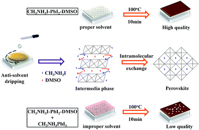 | ||
| Scheme 1 Schematic illustration for the formation process of CH3NH3PbI3 thin films made with different anti-solvents. | ||
Next, we recorded PL traces of CH3NH3PbI3 films on alumina presented in Fig. 4. PL traces feature a fast decay and a slow decay, which can be attributed to the surface component and bulk component related charge recombinations, respectively.43 Table S1† displays the kinetic parameters obtained through fitting the PL decays with a two exponential decay function. The time constants of the surface component and bulk component (4.5 ns and 42 ns for DCM; 5.1 ns and 57 ns for TL; 7.6 ns and 72 ns for DE) increase in the sequence DCM < TL < DE, suggesting the decreased trap-assisted recombination rate and trap density.44,45 A considerable long amplitude-averaged PL lifetime (62 ns) for the DE-treated film was obtained due to the improved film quality.
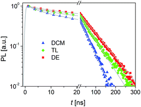 | ||
| Fig. 4 Normalized PL decay traces of CH3NH3PbI3 films on alumina. Excitation wavelength: 482 nm; probe wavelength: 760 nm. | ||
fs-TA was further employed to monitor the trap-assisted charge recombination in the early stage right after photoexcitation. Extensive Auger recombination was avoided through the power-dependent measurements shown in Fig. S1.† A short pass filter (750 nm) was also placed in the pathway of probe lights before the sample to avert the distortion of spectral features and dynamics, in virtue of the excitation of the band edge or tail states.45 The fs-TA spectra (Fig. 5a–c) of CH3NH3PbI3 films on alumina were measured with a 490 nm pump light. Two obvious spectral features centered at around 650 nm and 760 nm were assigned to the photo-induced excited state absorption (ESA) and photo-bleaching (PB) bands, respectively. A dual-conduction band model46 and dual excited state model47 have been proposed to explain the spectral feature in the fs-TA spectra. It is well known that the 760 nm centered PB band is mainly attributed to the direct band transition induced band filling.48 The red-shifting of the PB band and the narrowing of FWHM with time delay can also be explained well with the band-filling model.
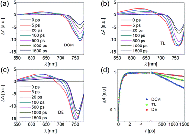 | ||
| Fig. 5 (a–c) fs-TA spectra of CH3NH3PbI3 films on alumina made with different anti-solvents: (a) DCM, (b) TL, and (c) DE. Pump wavelength: 490 nm; power fluence: 10 μJ cm−2. (d) Kinetic traces probed at 760 nm. The solid grey lines are fittings viaeqn (1). | ||
On account of the relatively low exciton binding energy of about a few millielectronvolts at room temperature,49 the species in the early stage after photoexcitation are predominantly free charges instead of bound excitons.50 Hence, the recovery kinetics of the PB band observed in our fs-TA spectra is mainly ascribed to the recombination of the photo-induced electrons and holes. The recovery kinetics at 760 nm (Fig. 5d) can be fitted using two exponential functions, including a rise exponential function and a decay exponential function convoluted with a Gaussian instrument response function (IRF),
ΔA = IRF ⊗ [(−A1)exp(−t/τrise) + A2![[thin space (1/6-em)]](https://www.rsc.org/images/entities/char_2009.gif) exp(−t/τdecay)], exp(−t/τdecay)], | (1) |
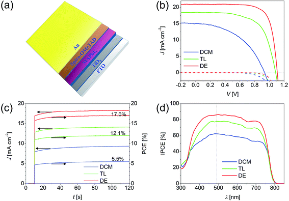
Subsequently, we fabricated perovskite solar cells to investigate the anti-solvent dependent device performance. The device structure, J–V curves, steady-state PCE output and incident-photon-to-current conversion efficiency (IPCE) spectra are shown in Fig. 6. The J–V curves were measured under an irradiance of 100 mW cm−2 stimulated AM1.5G sunlight and the parameters are tabulated in Table 2. The CH3NH3PbI3 solar cell with DE as the anti-solvent has a highest open-circuit photovoltage (VOC) of 1.11 V, a highest short-circuit photocurrent (JSC) of 20.95 mA cm−2, and a highest fill factor (FF) of 74.1%, generating the best performance with an average PCE of 17.2%, compared with those of TL (12.6%) and DCM (6.5%) treated cells. The tendency of PCEs obtained from the J–V curves is in good agreement with that of the steady-state PCE output. The values of VOC, JSC, and FF vary with anti-solvents, in the order DCM < TL < DE, so do the IPCE heights in the spectral range from 450 to 700 nm.
| Solvent | J SC [mA cm−2] | V OC [V] | FF [%] | PCE [%] |
|---|---|---|---|---|
| a Each value is the average of the data taken from 18 devices. | ||||
| DCM | 15.02 ± 1.75 | 0.94 ± 0.08 | 45.5 ± 6.9 | 6.5 ± 1.8 |
| TL | 18.49 ± 0.92 | 1.08 ± 0.02 | 63.4 ± 3.2 | 12.6 ± 1.4 |
| DE | 20.95 ± 0.85 | 1.11 ± 0.02 | 74.1 ± 3.5 | 17.2 ± 1.4 |
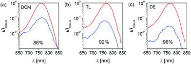
To unlock the anti-solvent dependent IPCE heights (86% for DE, 78% for TL, and 62% for DCM at 490 nm) of these perovskite solar cells, light-harvesting efficiency (Fig. S2†) was monitored through measuring the UV-vis absorption spectra of films on titania. All samples show almost 100% of light-harvesting efficiency at 490 nm. The PL spectra with or without an electron and hole extraction layer were further measured to reveal anti-solvent dependent charge dissociation.53 With the assumption that no electron can be injected into alumina from CH3NH3PbI3 due to a higher conduction band of alumina relative to that of CH3NH3PbI3, the PL of Al2O3/CH3NH3PbI3 mainly originates from the bulk recombination of photogenerated electrons and holes. Significant PL quenching can be probed for TiO2/CH3NH3PbI3/Spiro, signifying charge transfer occurring at the energy-offset TiO2/CH3NH3PbI3 and CH3NH3PbI3/Spiro interfaces. Hence, the charge-dissociation efficiency can be roughly estimated from the PL quenching efficiency, in the order DCM < TL < DE (Fig. 7). Highly efficient charge dissociation can be realized with DE as the anti-solvent.
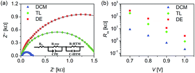
Finally, we measured the impedance spectroscopies of CH3NH3PbI3 solar cells. The impedance spectra in Fig. 8a exhibit non-standard semicircles superposed by two semicircles. Generally, the semicircle at high frequency is related to hole transportation, whereas the semicircle at low frequency is related to the bulk charge recombination of CH3NH3PbI3 or the interface charge recombination between CH3NH3PbI3 and titania.54,55 Recombination resistances were obtained via fitting the impedance spectroscopies with a simplified equivalent circuit (Fig. 8a). As presented in Fig. 8b, the recombination resistance decreases mono-exponentially as a function of forward potential bias. At a given bias, recombination resistance increases in the order DCM < TL < DE, which is well consistent with the VOC tendency.
Conclusions
To summarize, we have used DCM, TL, and DE as anti-solvents in the one-step deposition of CH3NH3PbI3 to tune the thin film quality and photovoltaic performance. The relative contents of intermediate and perovskite phases that coexisted in the as-prepared films have been determined by ATR-FTIR. It is found that a high content of an intermediate phase in the as-prepared film is favorable for the eventual formation of the CH3NH3PbI3 film with a large grain size and low defects in the subsequent thermal annealing. The CH3NH3PbI3 film made with DE as the anti-solvent has a long PL lifetime owing to the reduced trap-assisted recombination. Moreover, in a TiO2/CH3NH3PbI3/Spiro-OMeTAD solar cell the perovskite light absorption layer injects charges quantitatively to charge extraction layers and attenuates charge recombination effectively, leading to high device efficiency. Our work has revealed the intrinsic role of the intermediate phase in controlling the film quality of a solution processed organic–inorganic hybrid CH3NH3PbI3.Experimental section
Deposition of electron-transporting layer
An etched fluorine-doped tin oxide (FTO) conducting glass was ultrasonically cleaned with detergent, deionized water, acetone, and ethanol in turns for 10 min. The nitrogen dried FTO was further treated with UV-ozone for 20 min, immersed in a 40 mM TiCl4 aqueous solution at 70 °C for 90 min, rinsed with deionized water, and annealed at 500 °C for 30 min, so as to be coated with a compact TiO2 layer. Next, a mesoporous TiO2 layer was deposited on the compact TiO2 layer by spin coating for 30 s at 3000 rpm, using the commercial TiO2 paste (18NRT, Dyesol) diluted with anhydrous ethanol at a weight ratio of 1/3.5. After drying at 100 °C for 10 min, the TiO2 film was annealed at 500 °C for 30 min under dry air flow to remove organic components. Finally, the film was treated with 20 mM TiCl4 aqueous solution at 90 °C for 10 min, cleaned with deionized water, and annealed at 500 °C for 30 min. The thickness of the mesoporous titania layer is 200 ± 50 nm. Li-doping of TiO2 was carried out by spin coating 0.1 M LiTFSI in acetonitrile at 3000 rpm for 30 s with a ramp of 1000 rpm s−1, which was followed by another annealing step at 450 °C for 30 min according to the reported method.41Deposition of MAPbI3 perovskite layer
1.45 M of PbI2 (TCI, 99.99%) and MAI (Xi'an Polymer Light Technology Corp., 99.5%) were dissolved in DMSO under stirring at 70 °C for 60 min. After filtering with a PTFE syringe filter (pore diameter: 0.22 μm), the solution was kept at 70 °C as the TiO2 electrode. A CH3NH3PbI3 film was deposited by a consecutive two-step spin-coating process at 1000 rpm for 10 s and 5000 rpm for 30 s on the TiO2 electrode. At the time of 20 s prior to the program end, 0.8 mL of DE, TL, or DCM was dripped onto the spinning substrate. The films were then annealed at 100 °C for 10 min in a nitrogen-filled glove box.Deposition of hole-transporting layer and gold electrode
The filtered 60 mM Spiro-OMeTAD (Xi'an Polymer Light Technology Corp., 99.9%) in chlorobenzene was spin coated atop the annealed MAPbI3 films at 6000 rpm for 30 s. The molar ratios of the dopants are 0.5 for Li-TFSI, 0.1 for FK209, and 3.3 for TBP with respect to Spiro-OMeTAD. Finally, 60 nm-thick Au was thermally evaporated on top of the device under a vacuum of 1 × 10⁻⁴ Pa at a deposition rate of 0.01 nm s−1 for the first 5 nm, 0.03 nm s−1 for the next 15 nm, and 0.05 nm s−1 for the last 40 nm.Deposition of mesoporous Al2O3
Mesoporous alumina films for control measurements were deposited by spin coating of a diluted colloidal dispersion (5 wt%) of Al2O3 nanoparticles (Sigma-Aldrich) in isopropanol for 60 s at 6000 rpm, onto cleaned FTO described above. The films were dried at 150 °C for 10 min, and further annealed at 500 °C for 30 min under dry air flow. The thickness of the alumina layer was controlled to be almost the same as that of titania.ATR-FTIR, SEM, XRD, UV-vis, and PL measurements
ATR-FTIR spectra were collected with a Perkin Elmer FT-IR/NIR spectrometer (Frontier). Scanning electron microscopic images were recorded with a Hitachi S-4800 Instrument (Japan). The X-ray diffraction patterns were measured with a Bruker D8 FOCUS Powder X-ray Diffractometer (XRD) using Cu Kα radiation (λ = 0.15405 nm). UV-vis absorption spectra were recorded on a Perkin Elmer Lambda 900 spectrophotometer. Steady-state PL and time-resolved PL measurements were performed on a LifeSpec-II fluorescence spectrometer. The EPL485 laser diode was used to supply excitation light.EQE, J–V, and impedance spectroscopy measurements
The incident photon-to-electron conversion efficiency (IPCE) measurement was performed using a system combining a 150 W xenon lamp, a Zolix Omni-λ300 monochromator, a Keithley 2400 source meter and a Hamamatsu S1337-1010BQ silicon diode calibrated in National Institute of Metrology, China. The data were collected with a wavelength sampling interval of 10 nm and a current sampling time of 1 s under the full computer control. The cell performance evaluated by the current–voltage (J–V) measurements under simulated solar light (a model LS1000-4S-AM1.5G-1000W solar simulator, Solar Light Company, USA) with a light intensity of 100 mW cm−2, tested with a PMA2144 pyranometer and a calibrated PMA 2100 dose control system. The effective area was set to 0.04 cm2 (0.2 cm × 0.2 cm) by using a non-reflective metal mask. Impedance spectroscopies were recorded on an IM6ex electrochemical workstation in the dark by applying a 20 mV voltage perturbation over a series of forward bias, with the frequency range from 1 Hz to 1 MHz. The measured impedance spectra were further fitted using the Z-view software (v2.80, Scribner Associates Inc.).Femtosecond transient absorption measurements
For femtosecond optical spectroscopy, the laser source was a Spectra Physics Spitfire regenerative amplifier (130 fs, 1 kHz, 800 nm) seeded by a mode locked Spectra Physics Tsunami Ti: sapphire laser. The 800 nm laser was divided into two parts with a 9/1 beam splitter. The pump pulses were generated by a Light Conversion TOPAS-C optical parametric amplifier with the main part of the 800 nm laser, and then modulated with a phase-locked chopper. The white-light supercontinuum (440–1700 nm) probe pulse was generated by focusing the minor portion of the 800 nm laser onto a 4 mm-thick sapphire plate. The fluctuation of both pump and probe beams was cancelled out by measuring the unexcited sample with a reference pulse, an almost equal beam with the probe pulse. A 750 nm SPF has been placed on the probe path before the sample to avoid band-edge or tail-state pumping. The optical density changes at selected wavelengths were measured with the CDP2022i UV-vis multichannel detector with a pair of photodidode arrays. The fs-TA data collected with the ExciPRO software (CDP Corp.) and group-velocity dispersion of the white-light continuum have been corrected with the Surface Xplorer software (version 2.3) before kinetic analysis. More detailed information about the fs-TA system has been described in our previous article.56 All the films used for optical study were encapsulated under an inert atmosphere.Acknowledgements
The National 973 Program (2015CB932204) and the Key Technology R&D Program (BE2014147-1) of Science and Technology Department of Jiangsu Province have supported this work. We are grateful to Prof. Nam-Gyu Park and Dr Jin-Wook Lee for fruitful discussion on cell fabrication.References
- H.-S. Kim, C.-R. Lee, J.-H. Im, K.-B. Lee, T. Moehl, A. Marchioro, S.-J. Moon, R. Humphry-Baker, J.-H. Yum, J. E. Moser, M. Grätzel and N.-G. Park, Sci. Rep., 2012, 2, 591 Search PubMed.
- M. M. Lee, J. Teuscher, T. Miyasaka, T. N. Murakami and H. J. Snaith, Science, 2012, 338, 643 CrossRef CAS PubMed.
- J. Burschka, N. Pellet, S.-J. Moon, R. Humphry-Baker, P. Gao, M. K. Nazeeruddin and M. Grätzel, Nature, 2013, 499, 316 CrossRef CAS PubMed.
- M. Liu, M. B. Johnston and H. J. Snaith, Nature, 2013, 501, 395 CrossRef CAS PubMed.
- H. Zhou, Q. Chen, G. Li, S. Luo, T.-b. Song, H.-S. Duan, Z. Hong, J. You, Y. Liu and Y. Yang, Science, 2014, 345, 542 CrossRef CAS PubMed.
- N. J. Jeon, J. H. Noh, W. S. Yang, Y. C. Kim, S. Ryu, J. Seo and S. I. Seok, Nature, 2015, 517, 476 CrossRef CAS PubMed.
- W. S. Yang, J. H. Noh, N. J. Jeon, Y. C. Kim, S. Ryu, J. Seo and S. I. Seok, Science, 2015, 348, 1234 CrossRef CAS PubMed.
- W. Chen, Y. Wu, Y. Yue, J. Liu, W. Zhang, X. Yang, H. Chen, E. Bi, I. Ashraful, M. Grätzel and L. Han, Science, 2015, 350, 944 CrossRef CAS PubMed.
- X. Li, D. Bi, C. Yi, J.-D. Décoppet, J. Luo, S. M. Zakeeruddin, A. Hagfeldt and M. Grätzel, Science, 2016, 353, 58 CrossRef CAS PubMed.
- M. Saliba, T. Matsui, K. Domanski, J.-Y. Seo, A. Ummadisingu, S. M. Zakeeruddin, J.-P. Correa-Baena, W. R. Tress, A. Abate, A. Hagfeldt and M. Grätzel, Science, 2016, 354, 206 CrossRef CAS PubMed.
- N. J. Jeon, J. H. Noh, Y. C. Kim, W. S. Yang, S. Ryu and S. I. Seok, Nat. Mater., 2014, 13, 897 CrossRef CAS PubMed.
- H. Chen, Z. Wei, H. He, X. Zheng, K. S. Wong and S. Yang, Adv. Energy Mater., 2016, 6, 1502087 CrossRef.
- W. Li, J. Fan, J. Li, G. Niu, Y. Mai and L. Wang, ACS Appl. Mater. Interfaces, 2016, 8, 30107 CAS.
- J. H. Noh, S. H. Im, J. H. Heo, T. N. Mandal and S. I. Seok, Nano Lett., 2013, 13, 1764 CrossRef CAS PubMed.
- D. P. McMeekin, G. Sadoughi, W. Rehman, G. E. Eperon, M. Saliba, M. T. Hörantner, A. Haghighirad, N. Sakai, L. Korte, B. Rech, M. B. Johnston, L. M. Herz and H. J. Snaith, Science, 2016, 351, 151 CrossRef CAS PubMed.
- M. Saliba, T. Matsui, J.-Y. Seo, K. Domanski, J.-P. Correa-Baena, M. K. Nazeeruddin, S. M. Zakeeruddin, W. Tress, A. Abate, A. Hagfeldt and M. Grätzel, Energy Environ. Sci., 2016, 9, 1989 CAS.
- L. Zuo, Z. Gu, T. Ye, W. Fu, G. Wu, H. Li and H. Chen, J. Am. Chem. Soc., 2015, 137, 2674 CrossRef CAS PubMed.
- J. Min, Z.-G. Zhang, Y. Hou, C. O. R. Quiroz, T. Przybilla, C. Bronnbauer, F. Guo, K. Forberich, H. Azimi, T. Ameri, E. Spiecker, Y. Li and C. J. Brabec, Chem. Mater., 2015, 27, 227 CrossRef CAS.
- L. Liu, A. Mei, T. Liu, P. Jiang, Y. Sheng, L. Zhang and H. Han, J. Am. Chem. Soc., 2015, 137, 1790 CrossRef CAS PubMed.
- National Renewable Energy Laboratory, Best Research-Cell Efficiencies chart, http://www.nrel.gov/ncpv/images/efficiency_chart.jpg.
- M. Xiao, F. Huang, W. Huang, Y. Dkhissi, Y. Zhu, J. Etheridge, A. Gray-Weale, U. Bach, Y.-B. Cheng and L. Spiccia, Angew. Chem., Int. Ed., 2014, 53, 9898 CrossRef CAS PubMed.
- X. Li, M. I. Dar, C. Yi, J. Luo, M. Tschumi, S. M. Zakeeruddin, M. K. Nazeeruddin, H. Han and M. Grätzel, Nat. Chem., 2015, 7, 703 CrossRef CAS PubMed.
- W. Zhang, M. Saliba, D. T. Moore, S. K. Pathak, M. T. Hörantner, T. Stergiopoulos, S. D. Stranks, G. E. Eperon, J. A. Alexander-Webber, A. Abate, A. Sadhanala, S. Yao, Y. Chen, R. H. Friend, L. A. Estroff, U. Wiesner and H. J. Snaith, Nat. Commun., 2015, 6, 6142 CrossRef CAS PubMed.
- F. Wang, H. Yu, H. Xu and N. Zhao, Adv. Funct. Mater., 2015, 25, 1120 CrossRef CAS.
- L. Hu, J. Peng, W. Wang, Z. Xia, J. Yuan, J. Lu, X. Huang, W. Ma, H. Song, W. Chen, Y.-B. Cheng and J. Tang, ACS Photonics, 2014, 1, 547 CrossRef CAS.
- Y. Wu, A. Islam, X. Yang, C. Qin, J. Liu, K. Zhang, W. Peng and L. Han, Energy Environ. Sci., 2014, 7, 2934 CAS.
- S. A. Kulkarni, T. Baikie, P. P. Boix, N. Yantara, N. Mathews and S. Mhaisalkar, J. Mater. Chem. A, 2014, 2, 9221 CAS.
- L. Zheng, Y. Ma, S. Chu, S. Wang, B. Qu, L. Xiao, Z. Chen, Q. Gong, Z. Wu and X. Hou, Nanoscale, 2014, 6, 8171 RSC.
- H. Zhang, J. Mao, H. He, D. Zhang, H. L. Zhu, F. Xie, K. S. Wong, M. Grätzel and W. C. H. Choy, Adv. Energy Mater., 2015, 5, 1501354 CrossRef.
- H. Zhang, J. Cheng, D. Li, F. Lin, J. Mao, C. Liang, A. K.-Y. Jen, M. Grätzel and W. C. H. Choy, Adv. Mater., 2017 DOI:10.1002/adma.201604695.
- C.-W. Chen, H.-W. Kang, S.-Y. Hsiao, P.-F. Yang, K.-M. Chiang and H.-W. Lin, Adv. Mater., 2014, 26, 6647 CrossRef CAS PubMed.
- O. Malinkiewicz, C. Roldán-Carmona, A. Soriano, E. Bandiello, L. Camacho, M. K. Nazeeruddin and H. J. Bolink, Adv. Energy Mater., 2014, 4, 1400345 CrossRef.
- J.-W. Lee, H.-S. Kim and N.-G. Park, Acc. Chem. Res., 2016, 49, 311 CrossRef CAS PubMed.
- Y. Rong, S. Venkatesan, R. Guo, Y. Wang, J. Bao, W. Li, Z. Fan and Y. Yao, Nanoscale, 2016, 8, 12892 RSC.
- J. W. Jung, S. T. Williams and A. K.-Y. Jen, RSC Adv., 2014, 4, 62971 RSC.
- N. Ahn, D.-Y. Son, I.-H. Jang, S. M. Kang, M. Choi and N.-G. Park, J. Am. Chem. Soc., 2015, 137, 8696 CrossRef CAS PubMed.
- D.-Y. Son, J.-W. Lee, Y. J. Choi, I.-H. Jang, S. Lee, P. J. Yoo, H. Shin, N. Ahn, M. Choi, D. Kim and N.-G. Park, Nat. Energy, 2016 DOI:10.1038/nenergy.2016.81.
- N. Lin, J. Qiao, H. Dong, F. Ma and L. Wang, J. Mater. Chem. A, 2015, 3, 22839 CAS.
- K. Kara, D. A. Kara, C. Kırbıyık, M. Ersoz, O. Usluer, A. L. Briseno and M. Kus, RSC Adv., 2016, 6, 26606 RSC.
- C.-C. Chen, S. H. Chang, L.-C. Chen, C.-L. Tsai, H.-M. Cheng, W.-C. Huang, W.-N. Chen, Y.-C. Lu, Z.-L. Tseng, K. Y. Chiu, S.-H. Chen and C.-G. Wu, Sol. Energy Mater. Sol. Cells, 2017, 159, 583 CrossRef CAS.
- F. Giordano, A. Abate, J. P. C. Baena, M. Saliba, T. Matsui, S. H. Im, S. M. Zakeeruddin, M. K. Nazeeruddin, A. Hagfeldt and M. Grätzel, Nat. Commun., 2016, 7, 10379 CrossRef CAS PubMed.
- S. Y. Leblebici, L. Leppert, Y. Li, S. E. Reyes-Lillo, S. Wickenburg, E. Wong, J. Lee, M. Melli, D. Ziegler, D. K. Angell, D. F. Ogletree, P. D. Ashby, F. M. Toma, J. B. Neaton, I. D. Sharp and A. Weber-Bargioni, Nat. Energy, 2016, 1, 16093 CrossRef CAS.
- D. Shi, V. Adinolfi, R. Comin, M. Yuan, E. Alarousu, A. Buin, Y. Chen, S. Hoogland, A. Rothenberger, K. Katsiev, Y. Losovyj, X. Zhang, P. A. Dowben, O. F. Mohammed, E. H. Sargent and O. M. Bakr, Science, 2015, 347, 519 CrossRef CAS PubMed.
- W. Nie, H. Tsai, R. Asadpour, J.-C. Blancon, A. J. Neukirch, G. Gupta, J. J. Crochet, M. Chhowalla, S. Tretiak, M. A. Alam, H.-L. Wang and A. D. Mohite, Science, 2015, 347, 522 CrossRef CAS PubMed.
- T. C. Sum, N. Mathews, G. Xing, S. S. Lim, W. K. Chong, D. Giovanni and H. A. Dewi, Acc. Chem. Res., 2016, 49, 294 CrossRef CAS PubMed.
- G. Xing, N. Mathews, S. Sun, S. S. Lim, Y. M. Lam, M. Grätzel, S. Mhaisalkar and T. C. Sum, Science, 2013, 342, 344 CrossRef CAS PubMed.
- K. G. Stamplecoskie, J. S. Manser and P. V. Kamat, Energy Environ. Sci., 2015, 8, 208 CAS.
- J. S. Manser and P. V. Kamat, Nat. Photonics, 2014, 8, 737 CrossRef CAS.
- A. Miyata, A. Mitioglu, P. Plochocka, O. Portugall, J. T.-W. Wang, S. D. Stranks, H. J. Snaith and R. J. Nicholas, Nat. Phys., 2015, 11, 582 CrossRef CAS.
- C. X. Sheng, C. Zhang, Y. Zhai, K. Mielczarek, W. Wang, W. Ma, A. Zakhidov and Z. V. Vardeny, Phys. Rev. Lett., 2015, 114, 116601 CrossRef PubMed.
- H.-Y. Hsu, C.-Y. Wang, A. Fathi, J.-W. Shiu, C.-C. Chung, P.-S. Shen, T.-F. Guo, P. Chen, Y.-P. Lee and E. W.-G. Diau, Angew. Chem., Int. Ed., 2014, 53, 9339 CrossRef CAS PubMed.
- P. Piatkowski, B. Cohen, F. J. Ramos, M. D. Nunzio, M. K. Nazeeruddin, M. Grätzel, S. Ahmad and A. Douhal, Phys. Chem. Chem. Phys., 2015, 17, 14674 RSC.
- P. Docampo, J. M. Ball, M. Darwich, G. E. Eperon and H. J. Snaith, Nat. Commun., 2013, 4, 2761 Search PubMed.
- A. Dualeh, T. Moehl, N. Tétreault, J. Teuscher, P. Gao, M. K. Nazeeruddin and M. Grätzel, ACS Nano, 2014, 8, 362 CrossRef CAS PubMed.
- V. Gonzalez-Pedro, E. J. Juarez-Perez, W.-S. Arsyad, E. M. Barea, F. Fabregat-Santiago, I. Mora-Sero and J. Bisquert, Nano Lett., 2014, 14, 888 CrossRef CAS PubMed.
- L. Yang, Y. Ren, Z. Yao, C. Yan, W. Ma and P. Wang, J. Phys. Chem. C, 2015, 119, 980 CAS.
Footnote |
| † Electronic supplementary information (ESI) available: Details of film fabrication and characterization. See DOI: 10.1039/c7se00125h |
| This journal is © The Royal Society of Chemistry 2017 |

