A Cd-reduced hybrid buffer layer of CdS/Zn(O,S) for environmentally friendly CIGS solar cells†
Tanka Raj
Rana
a,
SeongYeon
Kim
a,
JunHo
Kim
 *a,
Kihwan
Kim
b and
Jae Ho
Yun
b
aDepartment of Physics, Incheon National University, 119 Academy-ro, Yeonsu-gu, Incheon 22012, Republic of Korea. E-mail: jhk@inu.ac.kr
bPhotovoltaic Laboratory, Korea Institute of Energy Research (KIER), 152 Gajeong-ro, Yuseong-gu, Daejeon 34129, Republic of Korea
First published on 8th September 2017
Abstract
For the fabrication of high efficiency Cu(In,Ga)Se2 (CIGS) solar cells, a CdS thin film is usually used as the buffer layer. However, since Cd is toxic and also a hazardous material for the environment, Cd-free or Cd-reduced buffer is required for the realization of CIGS solar cells as an environmentally friendly device. We fabricated a Cd-reduced hybrid buffer layer of CdS(Cd-treatment)/Zn(O,S), where CdS was prepared by dipping it into a CdS CBD solution for 2 min and Zn(O,S) was deposited by co-sputtering of ZnO and ZnS. The hybrid buffer provided an improved short circuit current and open circuit voltage and thus high power conversion efficiency. The best CIGS solar cell with the hybrid buffer showed 12.69% cell efficiency compared to the CdS-buffered standard cell with 13.06% cell efficiency. The improved efficiency of the Cd-treated solar cell was found to be a consequence of an enhanced response to blue wavelength photons and surface passivation of the absorber surface by the treatment.
1. Introduction
Among the thin film solar cells (TFSCs), CuIn1−xGaxSe2 (CIGS) solar cells have demonstrated the best power conversion efficiency (PCE) of 22.6% and the efficiency of CIGS solar cells has been rising gradually in recent years.1 High efficiency CIGS solar cells usually employ cadmium sulfide (CdS) as the buffer layer, which is deposited by chemical bath deposition (CBD) between the CIGS absorber and transparent front electrode. The CBD CdS layer has excellent properties for better device performances such as favorable band alignment both to CIGS and ZnO, protection of the absorber surface by complete coverage of its surface (due to close lattice matching) from the subsequent layer deposition process, and removal of natural oxides from the absorber surface by the CBD process.2–4 Moreover, Cd diffusion results in type inversion of CIGS to n-type,5 which induces an inherent pn junction over the CIGS absorber. However, cadmium causes serious environmental and biological problems, and hence a Cd free or low Cd content buffer layer below the restriction limit proposed by RoHS is desirable for the future photovoltaic (PV) market.6 Furthermore, CdS has the disadvantage of loss of carrier collection in a short wavelength region (350–550 nm) resulting in a lower current density due to its low band gap.7 Therefore, Cd-free buffer layers have attracted significant attention to develop environmentally friendly solar cell devices. Many Cd-free materials have been developed for alternative buffer layers such as In2S3, (Zn,Mg)O, (Zn,Sn)O, Zn(O,S), etc. with efficiencies more than 17%.8–15Zn(O,S), being a wide band gap and nontoxic material, is a promising candidate to replace CdS buffer. The CIGS with Zn(O,S) buffer showed an enhanced current density compared to CdS due to higher current collection in the spectral range of the blue wavelength.8–11 The band gap of Zn(O,S) can be tuned by the S/(S + O) ratio which provides an opportunity to adjust band alignment between the absorber and buffer layers. The CIGS solar cell with Zn(O,S) demonstrated a PCE over 18%, where the Zn(O,S) was fabricated in various ways such as CBD, sputtering and ALD.8–11 Despite the high efficiency of CBD Zn-based buffer, lower reproducibility and meta-stability were frequently observed in that device. The CBD grown Zn(S,O,OH) layer is usually composed of ZnO, ZnS and Zn(OH)2 (ref. 16), where the Zn(OH)2 phase is responsible for pinholes in the film and the light soaking effect of the device. The CBD process is not feasible for the systematic control of the chemical composition of sulfur and oxygen which have major influence on the barrier height in the vicinity of the absorber and buffer layers and thus the efficiency. Moreover, the solar cell with the solution-based Zn(S,O,OH) buffer layer needs post treatments such as annealing and light soaking at room temperature or higher temperature to reduce metastabilities.17,18 These additional treatments are undesirable for industrial scale production. Sputtering is an alternative method for Zn-based buffer deposition where the chemical composition can be controlled much systematically compared to CBD. We can deposit the Zn(O,S) film by rf sputtering, sputtering of the alloyed Zn(O,S) target and co-sputtering of ZnO and ZnS. The sputtering process allows vacuum inline production of solar cell devices which is favorable for commercial production of solar cells.
Cd-free buffer layers are being studied intensively, and PCEs comparable to that of CdS buffer are also achieved. However, CdS buffer is far better than other buffers in terms of stability and reproducibility. Therefore, considering the unique properties of CdS, we can use thin CdS combined with other buffers for stability and reproducibility. The passivation layer between the absorber and buffer can also be used to reduce the CdS thickness but the normal thickness of CdS in CIGS and CZTS is 50–80 nm.19,20 Now a days, the Cd material is also alloyed to reduce Cu/Zn disorder in CZTS as well as ZnxCd1−xS buffer also showed improvement for CZTS solar cells by improving the band alignment between buffer and absorber layers.21 There are many earlier reports on double buffered thin film solar cells like In2S3/CdS and Zn(O,S)/CdS where solar cell performances were superior to those of single buffered solar cells.22,23 In this work, we deposit an extremely thin CBD CdS layer prior to sputtering of Zn(O,S) which showed even higher efficiency comparable to CdS buffer. The device performance was very low with only a thin CdS layer due to inhomogeneity and pinhole formation in CdS films as in earlier reports.24 When we use thin CdS with Zn(O,S), we could use the advantages of CdS buffer and the wide band gap Zn(O,S) with high reduction of Cd. We deposited an extremely thin layer of CdS by the CBD process. Additional Zn(O,S) buffer was deposited by co-sputtering of Zn(O,S). The combined effect of these buffers showed enhancement in the photovoltaic conversion efficiency due to the improvement of the current density and open circuit voltage.
2. Results and discussion
Fig. 1 presents the FE-SEM surface images of bare CIGS, Cd-treated CIGS and CIGS covered with the CdS buffer layer. The morphology of the bare film shows well-crystalline CIGS grown with a larger grain size as shown in Fig. 1(a). For Cd-treatment, the dipping time of the absorber in solution was so short that only a slight difference between bare CIGS and Cd-treated CIGS morphologies was observed i.e. the surface of CIGS was barely covered by CdS. As the deposition time was increased, the CdS layer readily covered the CIGS surface. The complete coverage of CdS on the CIGS absorber was observed for 12 min deposition as shown in Fig. 1(c). The uniform CdS film grown on CIGS was used as the buffer layer for the reference solar cell whose estimated thickness was around ∼60 nm as shown in the inset in Fig. 1(c). XPS survey spectra of these samples are shown in Fig. 2. XPS results provide information on the chemical composition and chemical environment of atoms belonging to a thin layer or to the top surface of a specimen. It is a surface analysis technique of 2–10 atomic layer depth. Photoelectron signals detected from the survey spectra of the Cd-treated absorber were mixed with the signals of the CIGS absorber and CdS buffer layers. In addition to Cd signals, some elemental signals like Se, In, and Ga were also observed for the Cd-treated sample which implies that the thickness of CdS is not more than 10–20 nm (roughly). Importantly for device performance, ammonia washed out oxides from the absorber surface which was confirmed from the decreased intensity of the O 1S signals of the CdS and Cd-treated samples. The observed Na 1S peak in bare CIGS might be due to the diffusion of Na from the substrate (soda lime glass) to the absorber's surface during the CIGS deposition. But, it is dissolved during the Cd-treatment or CdS deposition. The removal of impurities of the CIGS surface by ammonia is commonly observed in the CBD CdS process. In the case of CdS deposited for 12 min, no elements from the CIGS absorber were detected whereas only Cd, S and O were detected due to the thick CdS layer.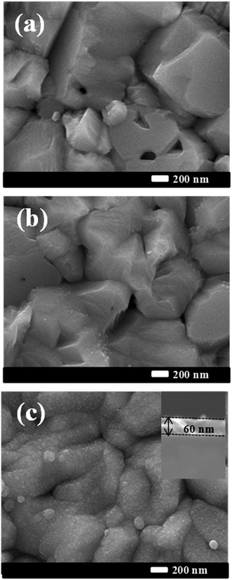 | ||
| Fig. 1 FE-SEM surface images of the bare CIGS absorber (a) CIGS after Cd-treatment (b) CIGS after the deposition of the CdS buffer layer (c). | ||
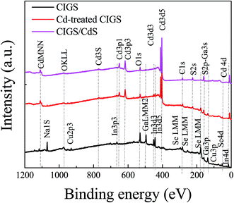 | ||
| Fig. 2 XPS survey spectra of bare CIGS, CIGS after Cd-treatment and deposition of CdS. For the Cd-treated sample, elements (In, Ga, and Se) from absorbers were detected along with Cd and S. | ||
The UV-Vis transmission spectra of the buffer layers grown on soda lime glass (SLG) are shown in Fig. 3(a). The CdS layer deposited for 2 min showed quite higher transmittance than the CdS reference layer. The transmission of CdS and CdS/Zn(O,S) films below 500 nm was reduced sharply, whereas Zn(O,S) and Cd-treated/Zn(O,S) showed higher transmission up to 400 nm due to the larger band gap of Zn(O,S). The higher transmission of Zn(O,S) and Cd-treated/Zn(O,S) in the blue wavelength region could enhance the current density of the device. Fig. 3(b) shows the plot of (αhν)2versus hν for the buffer layers, where the band gap is drawn by extrapolating the linear region of the curves to the X-axis. For band gap estimation, we used the equation αhν = C(hν − Eg)n where α is the absorption coefficient, C is a constant, and hν is the photon energy.25Eg is the bandgap energy, and n is a constant that takes a value of 2 for a direct transition and 0.5 for an indirect transition. The estimated band gaps of CdS, CdS/Zn(O,S), Zn(O,S) and Cd-treated/Zn(O,S) films were found to be 2.4 eV, 2.6 eV, 3.02 eV and 2.9 eV, respectively. Zn(O,S) and CdS showed band gaps very close to those of earlier reports.26,27 We found that the band gap of Cd-treated/Zn(O,S) was a little bit reduced from that of Zn(O,S), but the transmittance of the Cd-treated/Zn(O,S) above the optical band gap was almost the same as that of Zn(O,S). The XPS analysis of Zn(O,S) showed the ratio of S/(S + O) = 0.21, which was oxygen rich Zn(O,S). We also checked the crystal structure of Zn(O,S) by XRD. For XRD measurements, we prepared thick films (0.5 μm) for pure ZnS, pure ZnO and co-sputtered Zn(O,S). Pure ZnS has a zinc-blende structure with (111) preferential orientation at 2θ ∼ 28.5° whereas ZnO showed a wurtzite structure with dominant (002) orientation at 2θ ∼ 34° (Fig. S1†). Our oxygen rich Zn(O,S) film exhibits a wurtzite structure with dominant (002) orientation at 2θ ∼ 33° which is in close agreement with previously reported Zn(O,S) films,28 where the co-sputtered film showed a dominant peak at 2θ ∼ 32°. The Raman spectra of the ZnO film, which was measured with a UV excitation wavelength λ = 355 nm, showed a dominant peak at 582 cm−1 (A1(LO) mode) (Fig. S1†), while the ZnS film showed a dominant peak at 351 cm−1. The co-sputtered Zn(O,S) showed a main peak at 568 cm−1. Our Raman results are also similar to the previous results.29 From the XRD and Raman results, it is confirmed that the well-alloyed Zn(O,S) is formed by co-sputtering of ZnS and ZnO.
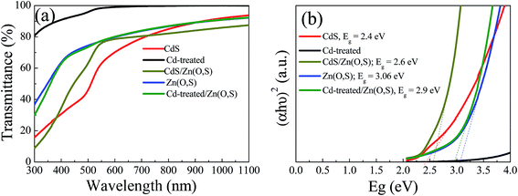 | ||
| Fig. 3 Transmittance spectra of CdS, Zn(O,S), CdS/Zn(O,S), and Cd-treated/Zn(O,S) (a) and band gaps of the respective films (b). | ||
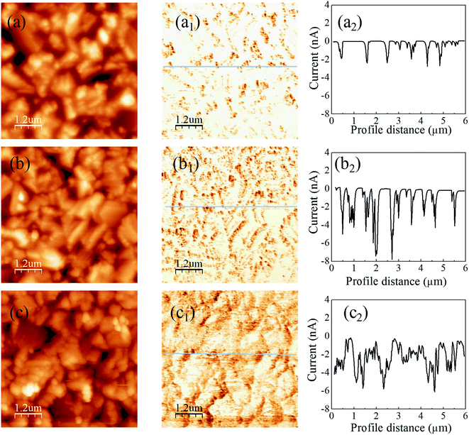
Fig. 4 shows the C-AFM images of the CIGS absorbers with different buffers, where the samples are prepared with the structure of glass/Mo/CIGS/buffer/i-ZnO and the buffers are Zn(O,S), Cd-treated/Zn(O,S) and CdS. The topography images of all samples are found to be similar. However, photocurrents that correspond to the dark region in the current mapping images reflect buffer-dependent characteristics. The photocurrent is generated by light illumination on the cantilever from the AFM laser diode (λ = ∼650 nm). For the sputtered Zn(O,S) on CIGS, the photocurrent is observed to be flowed through only some selected grain boundaries and it is zero in the grain interiors as seen in Fig. 4(a2). The dark region for the photocurrent path is increased in the Cd-treated/ZnS buffer sample (Fig. 4(b2)). The photo-current path regions are mostly enhanced for the CdS buffered absorber, which is shown in Fig. 4(c2). Fig. 4(c2) shows that photocurrents flow through almost all the area of the CdS buffered CIGS. To make it much clearer, we plot line profiles along the lines in the current mapping images. The current line profiles of the Zn(O,S) sample show low photocurrents (∼2 nA), whereas higher photocurrents (∼6 nA) are seen for the Cd-treated/Zn(O,S) and CdS samples. This result implies that the junction quality was the worst for the sputtered Zn(O,S) sample whereas simple Cd-treatment can cure the junction quality to achieve higher current collection. We believe that the low quality of Zn(O,S) buffered CIGS results from the plasma damage of the CIGS absorber layer during the Zn(O,S) sputtering, even though we applied low rf-power for the sputtering. By the Cd-treatment a very thin CdS layer is formed, by which some defects of the absorber are cured and the absorber layer is protected from plasma damage during the co-sputtering of Zn(O,S). To do a double check of this issue, we carried out TRPL measurements (shown in Fig. S4†) with the same samples as for the C-AFM. Here, the lifetime was extracted by using biexponential fitting of the decay curve.30 The average lifetime of charge carriers of the Zn(O,S) buffer sample is observed to be 0.93 ns. The lower lifetime of carriers is responsible for the low VOC of the solar cell device. The Cd-treated/Zn(O,S) sample shows an improved lifetime (1.16 ns) even though it is still lower than the carrier lifetime of the CdS sample (1.69 ns). The lifetime can be varied between ∼100 ns and ∼1 ns depending on the CIGS quality and measurement temperature;30,31 for example, it was measured to be ∼5 ns for CIGS showing a PCE of ∼15%.31 It was reported that the lifetime could be decreased from 250 ns to ∼1 ns by the air exposure of 1 day.32 Our samples were measured at room temperature and were exposed to air for a long time before the TRPL measurements. Hence, considering these facts, our lifetime results are acceptable.
For a higher PCE solar cell with single Zn(O,S) buffer, a preliminary study on the effect of sputtering conditions of Zn(O,S) on the solar cell efficiency is necessary. We varied the rf powers for the co-sputtering of ZnO and ZnS, and examined its effect on the cell efficiency. The device properties and J–V curves are summarized in Table S1 and in Fig. S3,† respectively. When we applied higher rf sputtering powers to deposit buffer, we usually observed a lower open circuit voltage (VOC) which could be due to the created defect states from the plasma damage. The possible plasma damage comes from the bombardment of high-energy negative oxygen ions and neutral particles during the sputtering process. The defect states induced by plasma-damage can act as charge recombination centers on the surface of the absorber layers. Therefore, lower rf power for the deposition of Zn-based buffer is desirable. However, even at the low rf power the Zn-based buffer solar cell showed quite lower efficiency than the CdS reference solar cell. This result implied that the interface between the absorber and buffer was carefully formed to improve the PCE. And this leads to Cd-treatment on the CIGS absorber prior to Zn(O,S) i.e., forming a double buffer layer of Cd-treated/Zn(O,S). The rf powers used to deposit the window (i-ZnO) and transparent conducting oxide (AZO/TCO) also have an influence on the performance of the completed solar cell.33 In our case, we used 40 W and 120 W rf powers to deposit i-ZnO and ITO for all fabricated solar cells, which is optimized to minimize some sputtering damage on the fabricated pn junction interface and to achieve higher ITO conductivity.
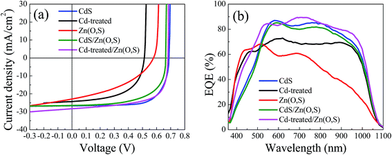
We fabricated CIGS solar cells with various buffers including Cd-treated/Zn(O,S). Fig. 5 shows the J–V curves and EQE curves of the fabricated solar cells, and Table 1 summarizes the device parameters. The solar cell with Cd-treated/Zn(O,S) showed good performance. Comparing the VOC values, the open circuit voltage (VOC) of the Cd-treated/Zn(O,S) solar cell was almost the same as that of the CdS buffered solar cell, whereas the current density (JSC) was the highest among them. The single Zn(O,S) buffered cell showed lower VOC (∼0.57 V), while the CdS reference cell showed a VOC of ∼0.69 V, which is slightly lower than that of the previously reported CdS reference cell. We believe that the difference of VOC among CdS reference cells is determined by the difference of the CIGS quality. Our CIGS films are exposed to air to somewhat extended time. The solar cells with a double buffer of CdS/Zn(O,S) and Cd-treated/Zn(O,S) showed a VOC of ∼0.66 V and ∼0.68 V, respectively. It is noted that the solar cell fabricated using the Cd-treated absorber without the Zn(O,S) buffer layer showed the lowest VOC. This result implies that the Cd-treated CIGS absorber was also damaged during the rf sputtering of i-ZnO and ITO, and furthermore, that the solar cell was not stable and easily degraded after a few days. The short circuit current density (JSC) for the single Zn(O,S) buffered solar cell is the lowest which is also due to the plasma damage during the sputtering of Zn(O,S). In addition, the larger conduction band off-set (CBO) between the absorber and buffer layers can be the cause of the low JSC. The highest JSC of the Cd-treated/Zn(O,S) could be attributed to the suitable CBO between the absorber and buffer layers and higher utilization of blue wavelength photons, which are seen from the higher FF and higher EQE values in the EQE curve. Thus, the device with Cd-treated/Zn(O,S) could show similar photovoltaic performance to the CdS reference solar cell. The PCE of the Cd-treated/Zn(O,S) cell (η = 12.69%) is comparable with that of the reference CdS cell (η = 13.06%). Fig. 5(b) shows the EQE curves of these devices in the wavelength region from 360 nm to 1180 nm. Solar cells with single Zn(O,S) and Cd-treated/Zn(O,S) show higher values of EQE in the short wavelength region (300–550 nm) compared to single CdS and double buffer CdS/Zn(O,S). The transition edges in the curve were observed to be ∼400 nm for ZnO and ∼510 nm for CdS and the double buffered solar cell, which corresponded to their estimated band gaps (Fig. S2†). The first derivative of the EQE with respect to wavelength is presented in Fig. S2,† where the band gaps of the CdS and CdS/Zn(O,S) are found to be ∼2.42 eV. For single Zn(O,S) buffer, the peak around ∼405 nm (∼3.06 eV) could be overlapped with the ZnO peak. These results are well matched with band gaps estimated from UV-Vis spectroscopy measurements. The CdS reference solar cell showed higher EQE than the double buffered CdS/Zn(O,S) one and as a consequence slightly higher JSC. EQE measurements showed much enhanced EQE in the entire wavelength for the Cd-treated/Zn(O,S) buffered solar cell, which enabled higher JSC.
| Device | V OC (V) | J SC (mA cm−2) | FF (%) | η (%) | R sh (Ω cm2) | R s (Ω cm2) |
|---|---|---|---|---|---|---|
| CdS | 0.69 | 26.67 | 71.27 | 13.06 | 757.57 | 3.87 |
| Cd-treated | 0.52 | 24.28 | 57 | 7.09 | 137.9 | 3.81 |
| Zn(O,S) | 0.58 | 22.05 | 44.83 | 5.73 | 70.49 | 7.7 |
| CdS/Zn(O,S) | 0.66 | 26.49 | 62.88 | 11.06 | 240.1 | 3.82 |
| Cd-treated/Zn(O,S) | 0.68 | 28.3 | 65.87 | 12.69 | 159.35 | 1.29 |
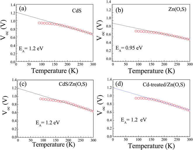
We measured the J–V characteristics of the solar cells in the temperature range of (300–90 K). The temperature dependence of the open circuit voltage (VOC) is shown in Fig. 6. We can draw important information on the dominant recombination by calculating the activation energy (EA) using the following formula.34
 | (1) |
The J–V result with different illumination lights for each buffer is shown in Fig. 7. No J–V distortions were observed for all types of solar cells at 300 K whereas a slight red-kink was noticed at 200 K for Zn(O,S). There is an electron barrier in the conduction band which is the sum of band bending potentials in the absorber, buffer and window layer. The crossover of dark and white J–V curves was observed only for Zn(O,S) at 200 K, which might be due to the electrical barrier associated with interfacial layers. The conduction band discontinuities between the absorber and buffer layers impede the thermionic emission current which results in the kink. The photogenerated electrons in the absorber should overcome the energy barrier by thermionic emission to be collected as the photocurrent. For the Zn(O,S) case, the magnitude of JSC was also observed to be decreased severely for 660 nm and 480 nm pass filter illumination cases, which is further evidence for the existence of the higher energy barrier at the pn junction interface, resulting in a kink and lower FF. These results are due to the deteriorated pn junction, which also originates from sputtering damage at the pn junction interface during the Zn(O,S) deposition. Thus, the damage is much reduced by adding Cd-treatment for the Cd-treated/Zn(O,S) solar cell, which shows an improved FF of J–V curves at low temperature as shown in Fig. 7d1.
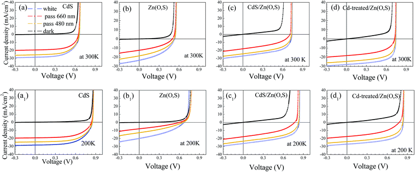 | ||
| Fig. 7 J–V curves of the fabricated solar cells with white, dark and filtered light illumination (pass 660 nm, 480 nm) measured at 300 K and 200 K. | ||
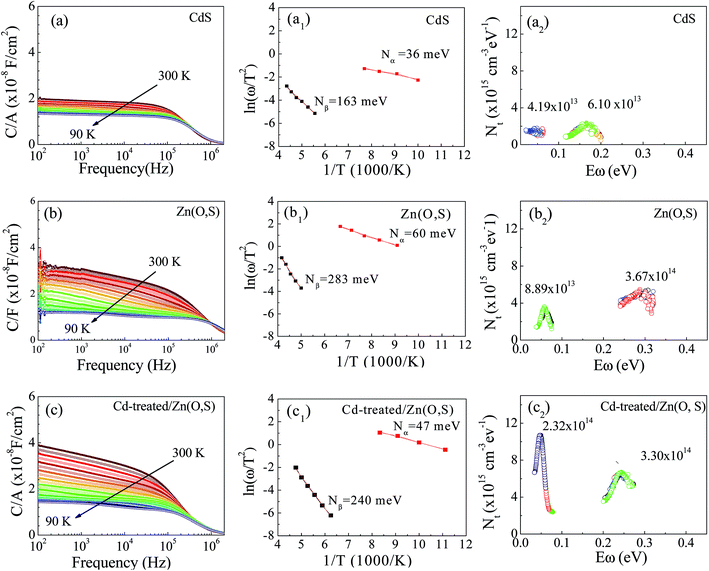
We performed AS measurements of the CdS reference solar cell, Zn(O,S) and Cd-treated/Zn(O,S) buffered solar cells. Fig. 8(a–c) represent C–f–T spectra of those cells at temperatures from 90 K to 300 K. The spectrum shows a capacitance step which indicates the defect level involved in the device. Fig. 8(a1–c1) show the Arrhenius plot which is fitted using the relationship of the inflection frequency ωo, the pre-exponential factor ϑo and the energy level of defects inside the band gap EA as given below.37,38
 | (2) |
The estimated values of EA from the linear plots show that all devices exhibit two trap levels derived from the higher and lower temperature regions, which are denoted as Nα and Nβ, respectively. The activation energy at 36 meV of the CdS reference solar cell is denoted as Nα, which is generally assigned to the shallow acceptors in CIGS originating from VCu.39 The trap levels with activation energies of 47 meV and 60 meV are Nα type defects for the Cd-treated/Zn(O,S) and Zn(O,S), respectively. There is no common consensus about the origin of Nα spectra. It is assigned to interfacial defects,40 bulk defects in CIGS,41 VSe42 and structural defects (In,Ga)Cu.43,44 The activation energies in the range of 50–200 meV are considered to be due to VSe donor states at the CIGS absorber surface having continuous energy distribution.40,42 Therefore, the defect signal of the reference solar cell at 163 meV could have originated from the VSe donor states at the CIGS absorber surface. The deep defect levels of Zn(O,S) and Cd-treated/Zn(O,S) were found to be 283 meV and 240 meV. These estimated energy values are found to be close to the InCu(0/+) and InCu(+/2+) level (240 meV and 350 meV).43 Different defect levels were observed for different buffer layers which are a consequence of inter-diffusion of elements in the absorber layer. The interfacial defects were also found to be buffer dependent. Moreover, the defect distribution in the absorber layer can be calculated by the following equation,41,42
 | (3) |
3. Conclusion
We fabricated CIGS solar cells with Zn(O,S), CdS, CdS/Zn(O,S) and Cd-treated/Zn(O,S) buffer layers. In the Cd-treated/Zn(O,S) buffer, 10–20 nm thick CdS was formed, which was much reduced from 60–80 nm for the reference CdS buffer. The lower VOC of the solar cell with Zn(O,S) in comparison with the CdS buffered solar cell could be compensated by applying CdS/Zn(O,S) double buffer and Cd-treated/Zn(O,S) buffer. Simple Cd-treatment was able (1) to reduce surface defects, (2) to protect the absorber from plasma damage during Zn(O,S) sputtering, and (3) to form improved CBO between the absorber and Zn(O,S). The transmittances of Cd-treated/Zn(O,S) were similar to those of Zn(O,S), which became beneficial for larger charge collection in the blue region than the CdS buffer layer, resulting in higher JSC. The Cd-treatment showed an improved FF in J–V curves at low temperatures as well as room temperature, which is also attributed to reduced damage at the pn junction interface during the Zn(O,S) sputtering. Thus, the Cd-treated/Zn(O,S) buffered solar cell showed 12.69% cell efficiency compared to the CdS-buffered standard cell with 13.06% cell efficiency. We believe that the Cd-reduced solar cell can be a significant achievement for environmentally friendly PV technology.4. Experimental section
The CdS buffer was deposited by using the CBD process according to the standard recipe45 where the CBD solution was composed of CdSO4 (0.0015 M) and thiourea (0.075 M) as Cd and S sources with the complexing agent NH4OH. For normal CdS, the CBD deposition time was 12 min whereas for Cd-treatment the deposition time was reduced to 2 min with remaining all parameters being constant. The Zn(O,S) buffer layer was deposited by co-sputtering of ZnO and ZnS at 160 °C substrate temperature. We varied the applied rf powers to the ZnO and ZnS target for tuning the elemental composition of S/(S + O) and used relatively low rf powers to minimize plasma damage because we found low PCE with higher rf powers.For the fabrication of solar cells, the co-evaporated CIGS film was used as the absorber layer. Briefly, the CIGS absorber layer was deposited by a three-stage process adopting the co-evaporation of In, Ga, Cu and Se. In the first stage, an approximately ∼1 μm thick (In,Ga)2Se3 precursor was deposited by co-evaporation of In, Ga, and Se at the substrate temperature of 350 °C. Then, Cu and Se were evaporated to form Cu-rich Cu(In,Ga)Se2 films (i.e., the second stage) at 550 °C. Finally, In, Ga, and Se were again added into the films to convert the Cu-rich Cu(In,Ga)Se2 film to the Cu-poor Cu(In,Ga)Se2 film at 550 °C (i.e., the third stage). The final compositions of the film were adjusted to Cu/(In + Ga) = 0.9 and Ga/(In + Ga) = 0.35, which were determined by EDS. The details of the device fabrication are available in our previous study.46 The CdS film was deposited by CBD as the buffer layer and annealed in air at 200 °C after deposition (for the reference cell). Zn(O,S) and hybrid type of buffer layers, Cd-treated/Zn(O,S) and CdS/Zn(O,S), were also deposited as buffer layers. After buffer layer deposition, i-ZnO (∼50 nm) and ITO (∼150 nm) were deposited by rf sputtering (40 W for i-ZnO, 120 W for ITO) subsequently. The fabrication process for window layers was the same as our previous report.47,48 The solar cells thus fabricated were scribed with a knife to obtain an effective area of ∼0.2 cm2.
The surface morphologies of bare CIGS and CdS deposited on CIGS were characterized by field emission scanning electron microscopy (FE-SEM) (JEOL JSM-7001F). The structural properties of the Zn(O,S) film were studied by X-ray diffraction (XRD) with a high resolution XRD machine (Rigaku, Smart LAB) equipped with a Cu-Kα source (λ = 1.5412 Å). Furthermore, a Raman spectrometer (Horiba, LabRAM HR800) was used to investigate the crystal structure of Zn(O,S) with an excitation laser of λ = 355 nm. Conductive atomic force microscope (C-AFM) measurements were performed in ambient air using a commercial AFM (Nanofocus, My-Scope). The same C-AFM samples were also characterized by using a time-resolved photoluminescence spectrometer (PicoQuanta, FluoTime 300 and MicroTime 100). For TRPL, a 633 nm laser with a 20 MHz repetition rate was used as an excitation source and a thermoelectric cooled NIR PMT (Hamamatsu H12397-75) was used to detect the decayed PL signal. The transmittance spectra of the films were measured by using an ultraviolet-visible (UV-Vis) spectrometer (Shimadzu UV-1600 (UV-16011pc)) to estimate their optical band gaps. X-ray photoelectron spectroscopy (XPS) was performed by using a PHI 5000 Versa Probe II. The current density–voltage (J–V) curve of the CIGS solar cell was obtained by using a source meter (Keithley 2400) under AM 1.5G filtered illumination of a 1000 W m−2 Xe lamp (Abet Technology), which was calibrated with the Si reference cell. The J–V characteristics were studied in the temperature range (300 K to 90 K) under dark, white and filtered light illumination. The external quantum efficiency (EQE) was measured by using a Xe light source and a monochromator combined with a light chopper and a lock-in amplifier (McScience Inc.). Admittance spectroscopy (AS) was performed to analyze the defects in the solar cells using a LCR meter (E4980A, Agilent) which probes from 20 Hz to 2 MHz in the temperature range of 300–90 K. All C–f scans were carried out at an ac voltage of 30 mV under the dark conditions. The same LCR meter was used to measure the capacitance–voltage (C–V) profile.
Conflicts of interest
There are no conflicts to declare.Acknowledgements
This work was supported by the National Research Foundation of Korea (NRF) funded by the Korean Government (NRF-2014R1A2A1A11053109, NRF-2016M1A2A2937010, and 2017R1A2B2006223).References
- P. Jackson, R. Wuerz, D. Hariskos, E. Lotter, W. Witte and M. Powalla, Phys. Status Solidi RRL, 2016, 10, 583–586 CrossRef CAS.
- W. Witte, S. Spiering and D. Hariskos, Vak. Forsch. Prax., 2014, 26, 23–27 CrossRef CAS.
- J. Kessler, K. O. Velthaus, M. Ruck, R. Laichinger, H. W. Schock, D. Lincot, R. Ortega and J. Vedel, 6th International Photovoltaic Solar Energy Conference, New Delhi, 1992, p. 1005 Search PubMed.
- L. Kronik, L. Burstein, M. Leibovitch, Y. Shapira, D. Gal, E. Moons, J. Beier, G. Hodes, D. Cahen, D. Hariskos, R. Klenk and H. W. Schock, Appl. Phys. Lett., 1995, 67, 1405–1407 CrossRef CAS.
- D. Abou-Ras, G. Kostorz, A. Romeo, D. Rudmann and A. N. Tiwari, Thin Solid Films, 2005, 480–481, 118–123 CrossRef CAS.
- R. L. Garris, L. M. Mansfield, B. Egaas and K. Ramanathan, IEEE J. Photovoltaics, 2017, 7, 281–285 CrossRef.
- J. M. Doña and J. Herrero, J. Electrochem. Soc., 1997, 144, 4091–4098 CrossRef.
- M. A. Contreras, T. Nakada, M. Hongo, A. O. Pudov and J. R. Sites, Proceedings of the 3rd World Conference on Photovoltaic Energy Conversion, Osaka, Japan, 2003, pp. 570–573 Search PubMed.
- D. Hariskos, R. Menner, P. Jackson, S. Paetel, W. Witte, W. Wischmann, M. Powalla, L. Burkert, T. Kolb, M. Oertel, B. Dimmler and B. Fuchs, Prog. Photovoltaics Res. Appl., 2012, 20, 534–542 CrossRef CAS.
- T. Kobayashi, Z. Jehl, L. Kao and T. Nakada, Proceedings of the 28th European Photovoltaic Solar Energy Conference, 2013, pp. 2199–2202 Search PubMed.
- R. Klenk, A. Steigert, T. Rissom, D. Greiner, C. A. Kaufmann, T. Unold and M. C. Lux-Steiner, Prog. Photovoltaics Res. Appl., 2013, 22, 161–165 CrossRef.
- S. Song, D. B. Khadka, S. Y. Kim, J. H. Kim, J. Gwak, J. H. Yun and K. Yoon, Curr. Appl Phys., 2014, 14, S17–S22 CrossRef.
- M. Powalla, W. Witte, P. Jackson, S. Paetel, E. Lotter, R. Wuerz, F. Kessler, C. Tschamber, W. Hempel, D. Hariskos, R. Menner, A. Bauer, S. Spiering, E. Ahlswede, T. M. Friedlmeier, D. Blazquez-Sanchez, I. Klugius and W. Wischmann, IEEE J. Photovoltaics, 2014, 4, 440–446 CrossRef.
- A. Hultqvist, C. Platzer-Bjorkman, T. Torndahl, M. Ruth and M. Edoff, Proceedings of the 22nd European Photovoltaic Solar Energy Conference, Milan, Italy, 2007, pp. 2381–2384 Search PubMed.
- J. Lindahl, U. Zimmermann, P. Szaniawski, T. Torndahl, A. Hultqvist, P. Salome, C. Platzer-Bjorkman and M. Edoff, IEEE J. Photovoltaics, 2013, 3, 1100–1105 CrossRef.
- T. Nakada and M. Mizutani, Proc. 28th IEEE Photovoltaic Specialist Conference, Anchorage, 2000, pp. 529–534 Search PubMed.
- K. Kushiya and O. Yamase, Jpn. J. Appl. Phys., 2000, 39, 2577–2582 CrossRef CAS.
- T. Nakada, T. Kobayashi, T. Kumazawa and H. Yamaguchi, IEEE J. Photovoltaics, 2013, 3, 461–466 CrossRef.
- M. T. Winkler, W. Wang, O. Gunawan, H. J. Hovel, T. K. Todorov and D. B. Mitzi, Energy Environ. Sci., 2014, 7, 1029–1036 Search PubMed.
- K. Orgassa, U. Rau, Q. Nguyen, H. W. Schock and J. H. Werner, Prog. Photovoltaics Res. Appl., 2002, 10, 457–463 CrossRef CAS.
- K. Sun, C. Yan, F. Liu, J. Huang, F. Zhou, J. A. Stride, M. Green and X. Hao, Adv. Energy Mater., 2016, 6, 1600046 CrossRef.
- J. Kim, H. Hiroi, T. K. Todorov, O. Gunawan, M. Kuwahara, T. Gokmen, D. Nair, M. Hopstaken, B. Shin, Y. S. Lee, W. Wang, H. Sugimoto and D. B. Mitzi, Adv. Mater., 2014, 26, 7427–7431 CrossRef CAS PubMed.
- D. H. Shin, L. Larina, K. H. Yoon and B. T. Ahn, Curr. Appl Phys., 2010, 10, 5142–5145 Search PubMed.
- M. A. Contreras, M. J. Romero, B. To, F. Hasoon, R. Noufi, S. Ward and K. Ramanathan, Thin Solid Films, 2002, 403–404, 204–211 CrossRef CAS.
- I. V. Pankove, Optical Processes in Semiconductors, Dover Inc., New York, 1975 Search PubMed.
- F. Lisco, P. M. Kaminski, A. Abbas, K. Bass, J. W. Bowers, G. Claudio, M. Losurdo and J. M. Walls, Thin Solid Films, 2015, 582, 323–327 CrossRef CAS.
- B. K. Meyer, A. Polity, B. Farangis, Y. He, D. Hasselkamp, T. Kramer and C. Wang, Appl. Phys. Lett., 2004, 85, 4929–4931 CrossRef CAS.
- M. Jaquez, K. M. Yu, M. Ting, M. Hettick, J. F. Sanchez-Royo, M. Welna, A. Javey, O. D. Dubon and W. Walukiewicz, J. Appl. Phys., 2015, 118, 2157021–2157027 CrossRef.
- M. Guc, M. Neuschitzer, D. Hariskos, A. Bauer, W. Witte, W. Hempel, L. CalvoBarrio, P. Pistor, A. Perez-Rodriguezad and V. Izquierdo-Rocaa, RSC Adv., 2016, 6, 24536–24542 RSC.
- I. L. Repins, W. K. Metzger, C. L. Perkins and J. V. Li, IEEE Trans. Electron Devices, 2010, 57, 2957–2963 CrossRef CAS.
- T. Gokmen, O. Gunawan, T. K. Todorov and D. B. Mitzi, Appl. Phys. Lett., 2013, 103, 103506 CrossRef.
- W. K. Metzger, I. L. Repins and M. A. Contreras, Appl. Phys. Lett., 2008, 93, 022110 CrossRef.
- D. H. Shin, J. H. Kim, Y. M. Shin, K. H. Yoon, E. A. Al-Ammar and B. T. Ahn, Prog. Photovoltaics Res. Appl., 2013, 21, 217–225 CrossRef CAS.
- V. Nadenau, U. Rau, A. Jasenek and H. W. Schock, J. Appl. Phys., 2000, 87, 584–593 CrossRef CAS.
- D. A. R. Barkhouse, O. Gunawan, T. K. Todorov and D. B. Mitzi, Prog. Photovoltaics Res. Appl., 2012, 20, 6–11 CrossRef CAS.
- T. K. Todorov, J. Tang, S. Bag, O. Gunawan, T. Gokmen, Y. Zhu and D. B. Mitzi, Adv. Energy Mater., 2013, 3, 34–38 CrossRef CAS.
- T. Walter, R. Herberholz, C. Muller and H. W. Schock, J. Appl. Phys., 1996, 80, 4411–4420 CrossRef CAS.
- H. S. Duan, W. Yang, B. Bob, C. J. Hsu, B. Lei and Y. Yang, Adv. Funct. Mater., 2013, 23, 1466–1471 CrossRef CAS.
- J. Vidal, S. Botti, P. Olsson, J. F. Guillemoles and L. Reining, Phys. Rev. Lett., 2010, 104, 56401 CrossRef PubMed.
- R. Herberholz, M. Igalson and H. W. Schock, J. Appl. Phys., 1998, 83, 318 CrossRef CAS.
- J. T. Heath, J. D. Cohen and W. N. Shafarman, J. Appl. Phys., 2004, 95, 1000 CrossRef CAS.
- T. Sakurai, N. Ishida, S. Ishizuka, M. M. Islam, A. Kasai, K. Matsubara, K. Sakurai, A. Yamada, K. Akimoto and S. Niki, Thin Solid Films, 2008, 516, 7036 CrossRef CAS.
- M. Igalson and M. Edoff, Thin Solid Films, 2005, 480, 322 CrossRef.
- Q. Cao, O. Gunawan, M. Copel, K. B. Reuter, S. J. Chey, V. R. Deline and D. B. Mitzi, Adv. Energy Mater., 2011, 1, 845–853 CrossRef CAS.
- K. Ramanathan, M. A. Contreras, C. L. Perkins, S. Asher, F. S. Hasoon, J. Keane, D. Young, M. Romero, W. Metzger, R. Noufi, J. Ward and A. Duda, Prog. Photovoltaics Res. Appl., 2003, 11, 225–230 CrossRef CAS.
- K. H. Kim, K. H. Yoon, J. H. Yun and B. T. Ahn, Electrochem. Solid-State Lett., 2006, 9, 382–385 CrossRef.
- D. B. Khadka, S. Y. Kim and J. H. Kim, J. Phys. Chem. C, 2016, 120, 4251–4258 CAS.
- T. R. Rana and J. H. Kim, Curr. Appl Phys., 2016, 16, 1666–1673 CrossRef.
Footnote |
| † Electronic supplementary information (ESI) available. See DOI: 10.1039/c7se00348j |
| This journal is © The Royal Society of Chemistry 2017 |

