
Band structure of the EuO/Si interface: justification for silicon spintronics†
L. L.
Lev
ab,
D. V.
Averyanov
b,
A. M.
Tokmachev
b,
F.
Bisti
a,
V. A.
Rogalev
a,
V. N.
Strocov
a and
V. G.
Storchak
*b
aSwiss Light Source, Paul Scherrer Institute, CH-5232 Villigen, Switzerland
bNational Research Centre “Kurchatov Institute”, Kurchatov Sq. 1, Moscow, 123182, Russia. E-mail: mussr@triumf.ca
First published on 23rd November 2016
Abstract
Semiconductor spintronics provides a framework for hybrid devices combining logic, communication and storage, circumventing limitations of the current electronics, especially with respect to the energy efficiency. Enormous efforts have been invested worldwide into the development of spintronics based on Si, the mainstream semiconductor platform. Notwithstanding remarkable pace, Si spintronics still experiences a technological bottleneck – creation of significant spin polarization in nonmagnetic Si. An emerging approach based on direct electrical spin injection from a ferromagnetic semiconductor – EuO being the prime choice – avoids problems inherent to metallic injectors. The functionality of the EuO/Si spin contact is controlled by the interface band alignment. To be competitive with charge electronics, the EuO/Si interface should exhibit a band offset which falls within the 0.5–2 eV range. We employ a soft-X-ray ARPES technique, using synchrotron radiation with photon energies around 1 keV, to probe the electronic structure of the buried EuO/Si interface with momentum resolution and chemical specificity. The band structure reveals a conduction band offset of 1.0 eV attesting the technological potential of the EuO/Si system.
Introduction
Scaling of conventional electronics faces formidable obstacles due to fundamental limits of information processing in different areas.1 The management of power consumption and heat generation is probably the main challenge. Spintronics, among other emerging technologies, addresses this issue by employing spin degrees of freedom. Metallic spintronic devices provide efficient data storage2 but transistor action requires semiconductors.3 In particular, Si spintronics4,5 is especially appealing due to the dominant role of Si in the modern electronics. As Si is non-magnetic, it requires creation of spin-polarized carriers in the system. Direct spin injection from a ferromagnetic (FM) metal into Si is ineffective due to the well-known impedance mismatch problem.6 Insulating tunnel barriers between an FM metal and silicon promote spin injection into bulk Si7,8 and Si nanotubes.9 Alternatives based on hot electrons,10 thermal11 and acoustic12 spin injection, and spin pumping13 are also available. However, spin injection characteristics sufficient for technological applications are yet to be demonstrated. Perhaps the solution is in the choice of a material integrated with Si and the quality of the integration itself: even FM tunnel contacts can be dramatically improved by replacing the material of the barrier14 or by advances in the growth procedure.15The impedance mismatch problem can be alleviated by using half-metallic injectors.16 However, the most straightforward approach is based on electrical injection of spins into Si from an FM semiconductor17 as it allows us to achieve the impedance match (e.g., by doping). Europium monoxide EuO is considered the best candidate for such a heterostructure due to its unique combination of the physical and technological properties. First, it is compatible with silicon: EuO is a binary compound with a rock-salt structure thermodynamically stable in contact with silicon;18 the band gap of EuO (1.1 eV) matches that of Si thus assisting the impedance match.19 Secondly, the remarkable bulk properties of EuO – a colossal magnetoresistivity of about 6 orders of magnitude in 2 T, a metal–insulator transition accompanied by up to 15 orders of magnitude change in resistivity, very strong magneto-optic effects, etc. – open ways for multi-functional devices. Thirdly, the magnetic properties of EuO can be tuned by doping,20,21 strain22 or optical pumping.23 Finally, EuO is a magnetically homogeneous on the nanoscale24 source of almost 100% spin-polarized electrons (due to its enormous exchange splitting 2ΔEex ∼ 0.6 eV)25 inviting spin-filter applications.26
These remarkable properties prompt numerous attempts to integrate EuO with different substrates27–30 as well as computational studies of the electronic structure of EuO21,31 and magnetic effects coming from interfacing EuO with other materials.32–34 However, direct epitaxial integration of EuO with Si turns out to be a notoriously difficult technological problem35–37 not only because of the significant lattice mismatch of 5.6%. Integration of crystalline oxides with Si is always challenging38 but the EuO synthesis is aggravated by interfacial chemistry: formation of higher oxides Eu3O4 and Eu2O3 as well as reactions of both Eu and oxygen with the substrate, in particular, leading to the formation of EuSi2.39 As a result, a layer of side products separates EuO and Si36,37 preventing the formation of the direct spin contact necessary for spintronics applications.
Recently, we proposed a new template for the growth of EuO (and other oxides) on Si suppressing unwanted chemistry at the interface and leading to direct epitaxial integration of the semiconductors.40,41 Moreover, analytical electron microscopy reveals that the interface engineering ensures an atomically sharp EuO/Si interface.42 Due to these advances in the growth methodology a clean direct EuO/Si interface free of any intermediate layer becomes available for studies of its functionality for spintronics applications.
The band structure at the interface (band bending and the resulting band offset) is the most important characteristic for the intended carrier injection. The band offset is often thought to be largely determined by work functions of the individual materials. If correct, it would mean that the conduction band of EuO is more than 2 eV higher in energy than that of Si.43 However, such estimates are often well off the mark,44 especially when ionic and covalent solids are interfaced. Unfortunately, at the moment there is no general theory of the energy lineups at semiconductor interfaces. The fundamental difficulty is the long range of the Coulomb interaction putting the positions of energy levels even deep in the bulk in strong dependence of the charge distribution at the interface.45,46 Numerous recent attempts to employ modern computational methods are mainly applied to lattice-matched systems with a known atomic structure (see, for example ref. 47 and 48). The basic problems of the EuO/Si system – (a) an unknown atomic structure of the interface and (b) a significant lattice mismatch leading to structural relaxation extending up to 5 monolayers40,49 – severely aggravate model calculations.
Angle-resolved photoemission spectroscopy (ARPES) is a direct technique to study the electronic structure of the surface layer with resolution in electron momentum k. ARPES has been previously used to probe the electronic structure of pristine EuO50 and Gd-doped EuO.51,52 The measurements reveal the Eu 4f band and the origin of the magnetism of EuO,50 the appearance of newly occupied states in the spectrum near the Fermi level EF due to Gd doping,51 as well as the evolution of the electronic structure through the FM metal–insulator transition.52 However, the electronic structure of the EuO/substrate interface – a major ingredient of a spintronic device – has not been addressed so far due to an extremely small probing depth of the conventional ARPES with photon energies hν around 100 eV employed in ref. 50–52. The EuO/Si interface is deeply buried within the grown structure due to a finite EuO film thickness and an additional thickness of the unavoidable capping layer protecting EuO from the atmosphere. Thus, the problem is highly challenging for ARPES.
Here we present the first study of the buried EuO/Si interface with soft-X-ray (SX) ARPES techniques employing synchrotron radiation with hν around 1 keV. The experiment hinges on a successful synthesis of ultrathin (5 monolayers) EuO films epitaxially integrated with Si and protected by a minimal (15–20 Å) capping layer of SiOx. Remarkably, the use of soft X-rays clearly exposes the bulk band dispersion of the substrate through about 30 Å of the combined EuO and SiOx overlayer. In combination with the energy position of the Eu2+ levels determined with resonant photoexcitation, it allows for a detailed study of the EuO and Si bands at the interface. Fortunately, in sharp contrast to simple estimates based on work functions of isolated EuO and Si, the experimental band alignment is highly encouraging for Si spintronics, suggesting that efficient injection of spin-polarized carriers from EuO into Si may be viable.
Results and discussion
The choice of ARPES techniques capable of assessing the buried interface is of paramount importance. Traditional ARPES employs the vacuum-ultraviolet (VUV) region making it an extremely surface sensitive probe: the probing depth characterized by the electron inelastic mean free path λ is only several Å.53 To avoid the measurement of surface-associated artifacts in situ sample transfer between the growth and analysis chambers is preferable. However, the vacuum coupling is technically difficult and the procedure precludes macroscopic characterization of the film before the measurement. An ex situ VUV-ARPES study of the EuO/Si system would require surface cleaning such as ion sputtering inevitably destroying the interface.The only reliable way to enhance the bulk and buried interface sensitivity is to utilize higher photon energies, where λ grows as [photoelectron kinetic energy]3/4. Higher energies bring further benefits: the uncertainty principle suggests that smearing in surface-perpendicular projection of k54 would decrease as 1/λ; a high kinetic energy of photoelectrons ensures that the final state can be approximated as a free electron.55 Although successful hard X-ray (HX-) ARPES studies in the multi-keV range (boosting λ up to 100 Å) have been reported for a number of materials55,56 the method is probably not advisable for the study of the EuO/Si system. First, the energy resolution gradually deteriorates with the increase of the photon energies. In the limit of high energy creation and annihilation of phonons can smear out the k specification of the final state.57 Moreover, in the multi-keV range the photoelectron momentum is not negligible and recoil effects become significant, especially for lighter atoms. Finally, the applications of HX-ARPES are much impeded by progressive reduction of the valence band (VB) cross-section.58 All these taken into account, SX-ARPES in the hν range around 1 keV seems to be the golden mean between VUV- and HX-ARPES for studies of the buried EuO/Si interface and similar systems. Moreover, monitoring of the resonance enhancement of valence states at the L- and M-absorption edges in this energy range enables the determination of the element-specific band structure. However, the problem requires pushing SX-ARPES to the limits of its energy resolution and probing depth. As for the sample prerequisites, the limitations of SX-ARPES set up severe restrictions on the film thickness. Thus, a fine balance between requirements stemming from the growth and ARPES methodologies is to be found. Preparation of the samples and the SX-ARPES setup are described in the Experimental section.
First, we have to establish that the SX-ARPES probing depth is sufficient to gain access to the EuO/Si interface and the Si substrate. The conclusion can be drawn from the photoemission (PE) response of the Si 2p core levels. Fig. 1 shows the angle-integrated PE spectrum measured at hν = 1300 eV. Being sensitive to the chemical state of Si atoms, this spectrum shows the characteristic 2p3/2–2p1/2 spin–orbit split doublet at the electron binding energies Eb = −98.7 and −99.5 eV identifying neutral Si atoms in the Si substrate, and a broad hump around Eb = −103.5 eV identifying positively charged Si ions in different oxygen environments in the non-stoichiometric SiOx capping layer (see, for example, ref. 59). The observation of a signal from Si0 is remarkable evidence that our SX-ARPES probing depth is sufficient to penetrate through the SiOx capping and reach the EuO/Si interface and the Si substrate. Moreover, a quantitative analysis of the relative integral intensities of the peaks (see the ESI†) has shown that within a practical sensitivity limit of 2% the probing depth extends as much as about 60 Å into the Si substrate.
 | ||
| Fig. 1 Si 2p core level spectrum measured at hν = 1300 eV. The doublet at higher Eb comes from neutral Si atoms of the substrate, while the broad peak at smaller Eb originates from positively charged Si ions of the capping layer. | ||
The next step is to get information on the EuO spin injector layer. First, we used X-ray absorption spectroscopy (XAS) with its large probing depth and elemental and chemical state specificity, allowing for discrimination of Eu ions with different oxidation numbers. The XAS spectrum at the Eu 3d5/2 absorption edge (Fig. 2a) reveals a dominant peak identified as Eu2+.60 It determines the prevailing stoichiometry of the EuO film, where most of EuO is intact and not oxidized by air. The Eu2+ peak is accompanied by smaller ones which can be identified as Eu3+.60 A small admixture of Eu3+ is not surprising since the amorphous capping layer is intentionally made extremely thin to enable the SX-ARPES study, with the side effect being the presence of a certain fraction of spatial regions with insufficient protection of EuO.
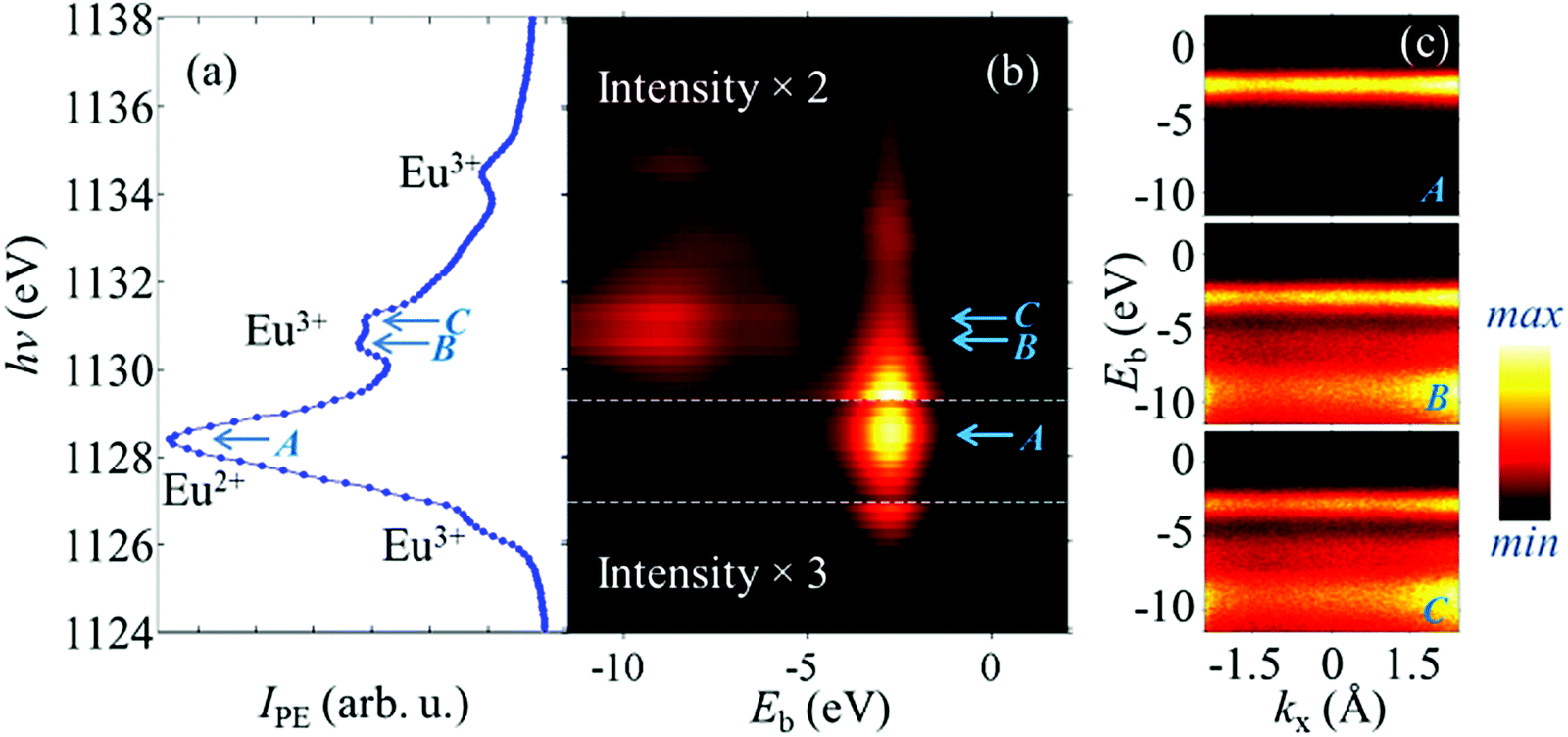 | ||
| Fig. 2 Resonant SX-ARPES at the Eu 3d5/2 edge. (a) XAS spectrum showing peaks corresponding to different oxidation states of Eu ions. (b) Angle-integrated IPE map showing the resonating Eu valence states. The map is split into three parts with different amplification of IPE. (c) Angle-resolved PE images at the main XAS peaks corresponding to hν values (A) 1128.4 eV, (B) 1130.6 eV and (C) 1131.0 eV. | ||
Furthermore, we probed the valence band region of the EuO layer with the element and chemical state specific resonant PE61,62 to get detailed information on Eu contributions in different oxidation states. Fig. 2b shows a resonant PE map of angle-integrated IPE(Eb,hν) measured through the VB region under variation of hν across the Eu 3d5/2 absorption edge. Tuning hν to different peaks of the XAS spectrum resonantly enhances the PE signal from Eu ions with the corresponding oxidation state, allowing thus chemical state resolution of the VB. In particular, the XAS peak at ∼1128.5 eV, corresponding to Eu2+ ions, manifests itself as a strong IPE(Eb,hν) resonant peak at Eb around −2.7 eV. Weaker XAS peaks, corresponding to Eu3+ ions discussed above, manifest themselves as weaker peaks in the Eb region from −12 to −6 eV. Fig. 2c shows angle-resolved PE images IPE(Eb,kx) measured at the Eu2+ and two strongest Eu3+ resonances. A narrow band centered at around −2.7 eV is the Eu2+ derived 7F0–7F6 multiplet. We do not detect any notable dispersion of Eu2+ or Eu3+ states, in accord with the highly localized character of Eu 4f electrons. Possible extremely weak dispersion effects near the top of the Eu2+ multiplet, caused by the admixture of delocalized O 2p orbitals and reported in the previous VUV-ARPES study,50 would be completely suppressed in our data because of a vanishing photoexcitation cross-section of O 2p compared to Eu 4f, especially at the Eu 3d resonance. The narrow energy width of the Eu2+ peak (Fig. 2c) certifies that charging effects in the thin EuO film are negligible. Indeed, spatial inhomogeneity of the charging over the sample would inevitably lead to spatially inhomogeneous energy level shifts which in turn would cause PE line broadening.
In our hν range around 1100 eV, photoelectrons from the VB region have Ek sufficiently high to escape into vacuum through the SiOx and EuO layers and bring spectroscopic information about the Si substrate. With the bulk lattice parameters of Si, tuning hν to 1120 eV brings kz (corrected for the X-ray photon momentum63) to the Γ-point of its 3D bulk Brillouin zone. Fig. 3a shows the resulting raw PE image IPE(Eb,kx) recorded at ky = 0, which corresponds therefore to the ΓKX direction. The image is dominated by Eu2+ and Eu3+ structures, and intense non-dispersive background arising mostly from the amorphous SiOx layer and photoelectrons from the Si substrate which smear their k-definition due to quasielastic scattering in the amorphous SiOx layer during their escape to vacuum. We can, however, discern sharp dispersions on top of the background. This spectral component can be enhanced by subtracting the non-dispersive one, shown in Fig. 3d, which is determined by integration of the IPE(Eb,kx) image over the intercepted kx interval. The enhanced E(k) in Fig. 3g immediately identifies the textbook light-hole and heavy-hole bands of bulk Si along ΓKX informed by photoelectrons penetrating through the SiOx and EuO layers. Detuning hν from 1120 eV results in a downward dispersion of the observed bands (not shown here for brevity) confirming the Γ-point location of our kz. Furthermore, Fig. 3b, e, h and c, f, i show similar results acquired at the same hν = 1120 eV (and thus kz in the Γ-point) but with different sample tilt angles (and thus different ky). They reflect the evolution of E(k) along off-symmetry directions parallel to ΓKX. We note that the sharpness of the observed Si bands rules out any significant space charge effects in our n-doped Si substrate. The response of the Si substrate can also be illustrated by maps of IPE(kx,ky) measured under continuous variation of the sample tilt (see the ESI†).
 | ||
| Fig. 3 Bands of bulk Si as spectroscopic fingerprints of the Si substrate. (a–c) PE images recorded at hν = 1120 eV for different sample tilts corresponding to ky = 0 (ΓKX direction), ky = 0.574 Å−1 and ky = 1.027 Å−1, respectively. (d–f) Angle-integrated spectra (a–c), respectively. (g–i) PE images (a–c) after corrections suppressing the non-dispersive contribution, respectively. | ||
Concluding our analysis of the SX-ARPES experimental data, we note that the observation of the coherent band structure signal from the Si substrate buried under a 30 Å overlayer of EuO and SiOx is a remarkable example of the probing capability of this technique.64 The standard X-ray photoelectron spectroscopy is hardly suitable in our case of the complex SiOx/EuO/Si film because, as apparent from Fig. 3d, e and f, the angle integration completely erodes the dispersive Si signal. Most important, however, fixed hν of laboratory X-ray sources permits neither resonant PE to determine the VB chemical composition, nor tuning kz required for navigation in the 3D k-space of the Si substrate.
Analysis of our results in Fig. 3g allows us to determine the main quantitative result of this work, the band offset at the EuO/Si interface critical for the spin injecting functionality of the EuO/Si spin contact. Fig. 4a shows the energy distribution curve (EDC) extracted from the image in Fig. 3g along kx = 0 and corresponding to the Γ-point of the bulk Brillouin zone. The two peaks in this EDC correspond to the VB maximum (VBM) of EuO and that of Si. Their energy difference estimates the band offset ΔEV between the two VBMs. However, in our case its estimate on the EuO side is aggravated by a multiplet structure of the Eu2+ derived 4f band forming the VBM. To determine the energy position of the upper 7F0 level, we fitted the experimental Eu2+ peak with a sequence of (experimental resolution limited) Gaussians, describing the 7F0–7F6 levels with their weights equal to 2J + 1 (J = 0–6) and the width and energy separation treated as fitting parameters. This fit placed the 7F0 multiplet level at −2.0 eV. The difference between this level and the VBM of Si positioned at −1.2 eV yields ΔEV ∼ 0.8 eV, as indicated in the band diagram shown in Fig. 4b. We emphasize that this exact result can only be achieved by combining the resonant and k-selective abilities of SX-ARPES, both requiring synchrotron radiation sources with tunable hν.
 | ||
| Fig. 4 (a) Experimental EDC extracted from Fig. 3a (hν = 1120 eV) corresponding to the Γ-point in Si. The two peaks are the VBM of EuO (7F0–7F6 multiplet) and that of Si. Indicated is their offset ΔEV = 0.8 eV. (b) Band diagram at the EuO/Si interface. It shows that the conduction band offset ΔEC between EuO in the FM state and Si is 1.0 eV. | ||
Injection of spins at the EuO/Si interface is expected to proceed from the conduction band (CB) of electron-doped EuO into that of Si. Although the corresponding CB offset ΔEC is not directly accessed by ARPES, in our case of a contact between paramagnetic EuO and Si it is unlikely to differ significantly from our ΔEV ∼ 0.8 eV because the experimentally established optical bandgaps of EuO in the paramagnetic state and Si are virtually the same (1.1 eV).65 Furthermore, electron doping of EuO either by oxygen deficiency or by trivalent rare-earth ions on the level of a few percent does not much affect the bandgap. In practice, spin injection requires ferromagnetic EuO where the exchange splitting of the CB minimum reduces the band gap to ∼0.9 eV65 and therefore increases ΔEC to ∼1.0 eV, as shown in Fig. 4b.
The determined value of ΔEC makes the EuO/Si interfaces a prospective system for silicon spintronics. The characteristic range of optimal supply voltage makes a rather narrow window: transistors cannot operate efficiently, on the one hand, at low supply voltage due to circuit reliability and noise issues and, on the other hand, at high voltage because the integrated circuit power consumption depends quadratically on the supply voltage. Therefore, supply voltage in electronic devices has been steadily decreasing for many years, but has recently stabilized at 0.5–2 V.1 Quite remarkably, the determined band offset of the EuO/Si spin contact structure falls within this optimal range. Although this fact turns out to be very encouraging, one inevitably confronts real problems in utilizing EuO as a spin injector in silicon spintronics. First, the EuO/Si interface should be free of any alien magnetic layer. In particular, uncontrolled inclusion of oxides, silicates or silicides which separate EuO and Si36,37 is highly detrimental for spin injection. Fortunately, recent advances in coupling EuO and Si ensure a chemically clean atomically abrupt EuO/Si interface free of any traces of unwanted magnetism.42 Second, spintronic applications assume effective spin injection into silicon at room temperature while EuO is ferromagnetic only up to 70 K. Although its ferromagnetism can be extended to higher temperatures, for example by doping,20,21 at the moment this route still has a gap of about 100 K with room temperature. Luckily, recent breakthroughs in utilizing proximity effects in EuS/FM metal heterostructures66,67 may indicate a viable route for a room temperature spin injection within the EuO/Si system. Finally, effective spin injection still requires its demonstration via electrical transport experiments.
Conclusions
In summary, we have explored the band structure of buried EuO/Si spin contacts. Our study used a novel synchrotron radiation based technique of SX-ARPES with hν around 1 keV, which offers a combination of an enhanced probing depth, selectivity in 3D electron momentum space, and elemental and chemical state specificity achieved through resonant photoexcitation. The EuO/Si contacts, tailored to match the probing depth of SX-ARPES, were grown with a 13 Å thick EuO layer and capped with a 17 Å thick SiOx layer. The electronic structure characteristic most critical for the spin injection functionality of the EuO/Si interface, the ΔEC band offset, is evaluated as 1.0 eV. Remarkably, this value falls within the optimal supply voltage range of modern electronic devices. This is a non-trivial result as estimates based on the work functions of isolated EuO and Si suggest the reverse order of the bands of EuO and Si with a band offset exceeding 2 eV. The current work thus suggests the application of EuO as a prospective spin injector into silicon.Experimental
Synthesis
The growth of ultrathin films of EuO is exceptionally difficult: standard approaches lead to layers of alien side product phases with thicknesses exceeding the required thickness of the EuO layer.36,37 Moreover, annealing procedures may lead to intermixing at the interface. Therefore, we employ a meticulously tailored growth scheme based on principles developed in ref. 40–42. The films are grown in a Riber Compact 12 system for molecular beam epitaxy of oxides. The substrates are n-Si (001) wafers with miscut angles not exceeding 0.5°. Doped n-Si is used to eliminate charging effects in the subsequent photoemission experiments. The natural surface oxide is removed by heating to reveal the standard 2 × 1 reconstruction of the clean Si(001) surface, monitored in situ with reflection high-energy electron diffraction (RHEED). This surface is highly reactive and requires protection before the oxide growth.The standard approach is to develop a submonolayer surface silicide.49 In practice, the saturated surface strontium silicide SrSi2 with 1 × 2 reconstruction is used (in the case of the EuO growth the isomorphous surface silicide EuSi2 is more appropriate). Regretfully, such protection is not sufficient for the growth of EuO directly on Si.37,40 Therefore, we employ another Eu surface silicide phase with a higher Eu content, seen as 1 × 5 reconstruction on RHEED images.40 It is formed on the Si surface exposed to a flux of Eu (4N) at 660 °C. One should take into account that the type and structure of the surface silicide used for protection may affect the interface band alignment68 although structural studies suggest oxidation of M–Si bonds and incorporation of the interfacial metal layer into the oxide system.69 EuO films are grown on the protected surface at a temperature of 340 ± 10 °C, an oxygen (6N) pressure of 6 × 10⁻⁹ Torr and a temperature of 500 ± 10 °C of the Eu effusion cell. The thickness of the films is limited to 5 monolayers – the minimum required for the lattice mismatch relaxation in the film.40,49 The FM transition temperature of these extremely ultrathin films is shifted to 10 K (measured by SQUID) due to enormous relaxation of the EuO lattice constant from 5.14 Å to 5.43 Å of the Si substrate. The film needs a capping layer because EuO reacts with atmospheric O2 and H2O. The routinely used protection by amorphous Eu2O340,41 is not suitable because it prevents control of the thickness of the EuO film and a large amount of Eu3+ hinders interpretation of the ARPES spectra. Therefore, we employ a capping layer of amorphous SiOx with a thickness of about 20 Å. Our experience based on X-ray diffraction and transmission electron microscopy studies is that the SiOx layer of such a thickness is sufficient for protection of the most part of the film but due to possible unevenness of the capping layer some regions of the EuO top surface may become oxidized to Eu2O3. Fortunately, this is not an obstacle for an SX-ARPES study of the band structure at the buried EuO/Si interface.
SX-ARPES
The general scheme of our SX-ARPES experiment on the SiOx/EuO/Si structures is presented in Fig. 5a. Monochromatic X-rays produced by the synchrotron eject photoelectrons from the SiOx, EuO and Si layers. The photoelectron analyzer detects their intensity distribution IPE(Ek,θ) as a function of the photoelectron kinetic energy Ek and emission angle θ which render into the binding energy Eb and momentum k of these electrons back in the valence band of the sample to yield its band structure E(k) as the electron binding energy Eb depending on momentum k. | ||
| Fig. 5 (a) A sketch of the SX-ARPES study of the EuO/Si interface. (b) Orientation of the experimental setup k-axes with respect to the Brillouin zone of Si. | ||
Our experiments have been carried out at the SX-ARPES endstation63 of the ADRESS beamline70 at the Swiss Light Source (Paul Scherrer Institute, Switzerland). We used p-polarization of incident X-rays. The experimental geometry63 with the slit of the photoelectron analyzer PHOIBOS-150 oriented along the incident beam sets the orientation of k-axes relative to the Brillouin zone of Si and EuO both of which have the fcc crystal structure as shown in Fig. 5b: the projection kx is directly measured through the emission angle along the analyzer slit, ky is varied by tilt rotation of the sample, and kz through hν. The experiments are carried out at the lowest available temperature of 12 K to quench thermal effects detrimental to the coherent k-resolved spectral component at high photoelectron energies.57 On the other hand, this temperature is above TC of our ultrathin film samples. The combined (beamline and analyzer) energy resolution was ∼0.2–0.25 eV. The position of EF was monitored by measurements at Au foil in electrical contact with the sample. No photon flux dependent charging effects were detected due to the small thickness of the film and n-doping of the Si substrate. The resonant SX-ARPES studies were complemented by X-ray absorption spectra measurements carried out in the total electron yield.
Acknowledgements
This work was partially supported by NRC “Kurchatov Institute”, Russian Foundation for Basic Research through grants 16-07-00204 and 16-29-03027, Russian Science Foundation through grant 14-19-00662, and Swiss National Science Foundation through project 200021_146890. We thank D. V. Vyalikh and M. B. Tsetlin for discussions, T. Schmitt for beamline support, and A. L. Vasiliev and A. N. Taldenkov for sample characterization.Notes and references
- I. L. Markov, Nature, 2014, 512, 147 CrossRef CAS PubMed
.
- A. Fert, Rev. Mod. Phys., 2008, 80, 1517 CrossRef CAS
- D. D. Awschalom and M. E. Flatté, Nat. Phys., 2007, 3, 153 CrossRef CAS
- R. Jansen, Nat. Mater., 2012, 11, 400 CrossRef CAS PubMed
- V. Sverdlov and S. Selberherr, Phys. Rep., 2015, 585, 1 CrossRef CAS
- G. Schmidt, D. Ferrand, L. W. Molenkamp, A. T. Filip and B. J. van Wees, Phys. Rev. B: Condens. Matter Mater. Phys., 2000, 62, R4790 CrossRef CAS
- B. T. Jonker, G. Kioseoglou, A. T. Hanbicki, C. H. Li and P. E. Thompson, Nat. Phys., 2007, 3, 542 CrossRef CAS
- S. P. Dash, S. Sharma, R. S. Patel, M. P. de Jong and R. Jansen, Nature, 2009, 462, 491 CrossRef CAS PubMed
- O. M. J. van't Erve, A. L. Friedman, C. H. Li, J. T. Robinson, J. Connell, L. J. Lauhon and B. T. Jonker, Nat. Commun., 2015, 6, 7541 CrossRef PubMed
- I. Appelbaum, B. Huang and D. J. Monsma, Nature, 2007, 447, 295 CrossRef CAS PubMed
- J. C. Le Breton, S. Sharma, H. Saito, S. Yuasa and R. Jansen, Nature, 2011, 475, 82 CrossRef CAS PubMed
- K. Uchida, H. Adachi, T. An, T. Ota, M. Toda, B. Hillebrands, S. Maekawa and E. Saitoh, Nat. Mater., 2011, 10, 737 CrossRef CAS PubMed
- E. Shikoh, K. Ando, K. Kubo, E. Saitoh, T. Shinjo and M. Shiraishi, Phys. Rev. Lett., 2013, 110, 127201 CrossRef PubMed
- O. M. J. van't Erve, A. L. Friedman, E. Cobas, C. H. Li, J. T. Robinson and B. T. Jonker, Nat. Nanotechnol., 2012, 7, 737 CrossRef PubMed
- A. Dankert, R. S. Dulal and S. P. Dash, Sci. Rep., 2013, 3, 3196 Search PubMed
- R. Farshchi and M. Ramsteiner, J. Appl. Phys., 2013, 113, 191101 CrossRef
- Y. Ohno, D. K. Young, B. Beschoten, F. Matsukura, H. Ohno and D. D. Awschalom, Nature, 1999, 402, 790 CrossRef CAS
- K. J. Hubbard and D. G. Schlom, J. Mater. Res., 1996, 11, 2757 CrossRef CAS
- C. Caspers, A. Gloskovskii, M. Gorgoi, C. Besson, M. Luysberg, K. Z. Rushchanskii, M. Ležaić, C. S. Fadley, W. Drube and M. Müller, Sci. Rep., 2016, 6, 22912 CrossRef CAS PubMed
- T. Mairoser, F. Loder, A. Melville, D. G. Schlom and A. Schmehl, Phys. Rev. B: Condens. Matter Mater. Phys., 2013, 87, 014416 CrossRef
- N. Jutong, U. Eckern, Th. Mairoser and U. Schwingenschlögl, Sci. Rep., 2015, 5, 8038 CrossRef CAS PubMed
- N. J. C. Ingle and I. S. Elfimov, Phys. Rev. B: Condens. Matter Mater. Phys., 2008, 77, 121202(R) CrossRef
- M. Matsubara, A. Schroer, A. Schmehl, A. Melville, C. Becher, M. Trujillo-Martinez, D. G. Schlom, J. Mannhart, J. Kroha and M. Fiebig, Nat. Commun., 2015, 6, 6724 CrossRef CAS PubMed
- V. G. Storchak, D. G. Eshchenko, E. Morenzoni, N. Ingle, W. Heiss, Th. Schwarzl, G. Springholz, R. L. Kallaher and S. von Molnár, Phys. Rev. B: Condens. Matter Mater. Phys., 2010, 81, 153201 CrossRef
- P. G. Steeneken, L. H. Tjeng, I. Elfimov, G. A. Sawatzky, G. Ghiringhelli, N. B. Brookes and D.-J. Huang, Phys. Rev. Lett., 2002, 88, 047201 CrossRef CAS PubMed
- G.-X. Miao and J. S. Moodera, Phys. Chem. Chem. Phys., 2015, 17, 751 RSC
- A. Schmehl, V. Vaithyanathan, A. Herrnberger, S. Thiel, Ch. Richter, M. Liberati, T. Heeg, M. Röckerath, L. F. Kourkoutis, S. Mühlbauer, P. Böni, D. A. Muller, Y. Barash, J. Schubert, Y. Idzerda, J. Mannhart and D. G. Schlom, Nat. Mater., 2007, 6, 882 CrossRef CAS PubMed
- R. Sutarto, S. G. Altendorf, B. Coloru, M. Moretti Sala, T. Haupricht, C. F. Chang, Z. Hu, C. Schüßler-Langeheine, N. Hollmann, H. Kierspel, H. H. Hsieh, H.-J. Lin, C. T. Chen and L. H. Tjeng, Phys. Rev. B: Condens. Matter Mater. Phys., 2009, 79, 205318 CrossRef
- S. Cao, P. Liu, J. Tang, H. Lu, C.-W. Bark, S. Ryu, C. B. Eom, A. Gruverman and P. A. Dowben, Appl. Phys. Lett., 2013, 102, 172402 CrossRef
- Th. Mairoser, J. A. Mundy, A. Melville, D. Hodash, P. Cueva, R. Held, A. Glavic, J. Schubert, D. A. Muller, D. G. Schlom and A. Schmehl, Nat. Commun., 2015, 6, 7716 CrossRef CAS PubMed
- A. M. Tokmachev, O. E. Parfenov and V. G. Storchak, Phys. Chem. Chem. Phys., 2014, 16, 18513 RSC
- H. Zhang, J. Wang, G. Xu, Y. Xu and S.-C. Zhang, Phys. Rev. Lett., 2014, 112, 096804 CrossRef PubMed
- Q. Zhang, S. A. Yang, W. Mi, Y. Cheng and U. Schwingenschlögl, Adv. Mater., 2016, 28, 959 CrossRef CAS PubMed
- Y. Song and G. Dai, Appl. Phys. Lett., 2015, 106, 223104 CrossRef
- J. N. Beukers, J. E. Kleibeuker, G. Koster, D. H. A. Blank, G. Rijnders, H. Hilgenkamp and A. Brinkman, Thin Solid Films, 2010, 518, 5173 CrossRef CAS
- C. Caspers, S. Flade, M. Gorgoi, A. Gloskovskii, W. Drube, C. M. Schneider and M. Müller, J. Appl. Phys., 2013, 113, 17C505 CrossRef
- J. A. Mundy, D. Hodash, A. Melville, R. Held, Th. Mairoser, D. A. Muller, L. F. Kourkoutis, A. Schmehl and D. G. Schlom, Appl. Phys. Lett., 2014, 104, 091601 CrossRef
- J. W. Reiner, A. M. Kolpak, Y. Segal, K. F. Garrity, S. Ismail-Beigi, C. H. Ahn and F. J. Walker, Adv. Mater., 2010, 22, 2919 CrossRef CAS PubMed
- D. V. Averyanov, A. M. Tokmachev, C. G. Karateeva, I. A. Karateev, E. F. Lobanovich, G. V. Prutskov, O. E. Parfenov, A. N. Taldenkov, A. L. Vasiliev and V. G. Storchak, Sci. Rep., 2016, 6, 25980 CrossRef CAS PubMed
- D. V. Averyanov, Y. G. Sadofyev, A. M. Tokmachev, A. E. Primenko, I. A. Likhachev and V. G. Storchak, ACS Appl. Mater. Interfaces, 2015, 7, 6146 CAS
- D. V. Averyanov, A. M. Tokmachev, I. A. Likhachev, E. F. Lobanovich, O. E. Parfenov, E. M. Pashaev, Y. G. Sadofyev, I. A. Subbotin, S. N. Yakunin and V. G. Storchak, Nanotechnology, 2016, 27, 045703 CrossRef PubMed
- D. V. Averyanov, Ch. G. Karateeva, I. A. Karateev, A. M. Tokmachev, A. L. Vasiliev, S. I. Zolotarev, I. A. Likhachev and V. G. Storchak, Sci. Rep., 2016, 6, 22841 CrossRef CAS PubMed
- D. E. Eastman, Phys. Rev. B: Condens. Matter Mater. Phys., 1973, 8, 6027 CrossRef CAS
- H. Kroemer, Rev. Mod. Phys., 2001, 73, 783 CrossRef CAS
- C. G. Van de Walle and R. M. Martin, Phys. Rev. B: Condens. Matter Mater. Phys., 1987, 35, 8154 CrossRef CAS
- A. Franciosi and C. G. Van de Walle, Surf. Sci. Rep., 1996, 25, 1 CrossRef CAS
- R. T. Tung and L. Kronik, Phys. Rev. B: Condens. Matter Mater. Phys., 2016, 94, 075310 CrossRef
- Y. Hinuma, A. Grüneis, G. Kresse and F. Oba, Phys. Rev. B: Condens. Matter Mater. Phys., 2014, 90, 155405 CrossRef
- R. A. McKee, F. J. Walker and M. F. Chisholm, Phys. Rev. Lett., 1998, 81, 3014 CrossRef CAS
- H. Miyazaki, T. Ito, H. J. Im, S. Yagi, M. Kato, K. Soda and S. Kimura, Phys. Rev. Lett., 2009, 102, 227203 CrossRef CAS PubMed
- J. A. C. Santana, J. M. An, N. Wu, K. D. Belashchenko, X. Wang, P. Liu, J. Tang, Y. Losovyj, I. N. Yakovkin and P. A. Dowben, Phys. Rev. B: Condens. Matter Mater. Phys., 2012, 85, 014406 CrossRef
- D. E. Shai, A. J. Melville, J. W. Harter, E. J. Monkman, D. W. Shen, A. Schmehl, D. G. Schlom and K. M. Shen, Phys. Rev. Lett., 2012, 108, 267003 CrossRef CAS PubMed
- C. J. Powell, A. Jablonski, I. S. Tilinin, S. Tanuma and D. R. Penn, J. Electron Spectrosc. Relat. Phenom., 1999, 98–99, 1 CrossRef CAS
- V. N. Strocov, J. Electron Spectrosc. Relat. Phenom., 2003, 130, 65 CrossRef CAS
- A. X. Gray, C. Papp, S. Ueda, B. Balke, Y. Yamashita, L. Plucinski, J. Minár, J. Braun, E. R. Ylvisaker, C. M. Schneider, W. E. Pickett, H. Ebert, K. Kobayashi and C. S. Fadley, Nat. Mater., 2011, 10, 759 CrossRef CAS PubMed
- A. X. Gray, J. Minár, S. Ueda, P. R. Stone, Y. Yamashita, J. Fujii, J. Braun, L. Plucinski, C. M. Schneider, G. Panaccione, H. Ebert, O. D. Dubon, K. Kobayashi and C. S. Fadley, Nat. Mater., 2012, 11, 957 CrossRef CAS PubMed
- J. Braun, J. Minár, S. Mankovsky, V. N. Strocov, N. B. Brookes, L. Plucinski, C. M. Schneider, C. S. Fadley and H. Ebert, Phys. Rev. B: Condens. Matter Mater. Phys., 2013, 88, 205409 CrossRef
- J. J. Yeh and I. Lindau, At. Data Nucl. Data Tables, 1985, 32, 1 CrossRef CAS
- Z. H. Lu, J. P. McCaffrey, B. Brar, G. D. Wilk, R. M. Wallace, L. C. Feldman and S. P. Tay, Appl. Phys. Lett., 1997, 71, 2764 CrossRef CAS
- K. Yamamoto, K. Horiba, M. Taguchi, M. Matsunami, N. Kamakura, A. Chainani, Y. Takata, K. Mimura, M. Shiga, H. Wada, Y. Senba, H. Ohashi and S. Shin, Phys. Rev. B: Condens. Matter Mater. Phys., 2005, 72, 161101(R) CrossRef
- S. L. Molodtsov, M. Richter, S. Danzenbächer, S. Weiling, L. Steinbeck and C. Laubschat, Phys. Rev. Lett., 1997, 78, 142 CrossRef CAS
- M. Kobayashi, I. Muneta, Y. Takeda, Y. Harada, A. Fujimori, J. Krempaský, T. Schmitt, S. Ohya, M. Tanaka, M. Oshima and V. N. Strocov, Phys. Rev. B: Condens. Matter Mater. Phys., 2014, 89, 205204 CrossRef
- V. N. Strocov, X. Wang, M. Shi, M. Kobayashi, J. Krempasky, C. Hess, T. Schmitt and L. Patthey, J. Synchrotron Radiat., 2014, 21, 32 CrossRef CAS PubMed
- M. Kobayashi, I. Muneta, Th. Schmitt, L. Patthey, S. Ohya, M. Tanaka, M. Oshima and V. N. Strocov, Appl. Phys. Lett., 2012, 101, 242103 Search PubMed
- J. Schoenes and P. Wachter, Phys. Rev. B: Condens. Matter Mater. Phys., 1974, 9, 3097 CrossRef CAS
- S. D. Pappas, P. Poulopoulos, B. Lewitz, A. Straub, A. Goschew, V. Kapaklis, F. Wilhelm, A. Rogalev and P. Fumagalli, Sci. Rep., 2013, 3, 1333 CAS
- P. Poulopoulos, A. Goschew, V. Kapaklis, M. Wolff, A. Delimitis, F. Wilhelm, A. Rogalev, S. D. Pappas, A. Straub and P. Fumagalli, Appl. Phys. Lett., 2014, 104, 112411 CrossRef
- R. A. McKee, F. J. Walker, M. B. Nardelli, W. A. Shelton and G. M. Stocks, Science, 2003, 300, 1726 CrossRef CAS PubMed
- Y. Segal, J. W. Reiner, A. M. Kolpak, Z. Zhang, S. Ismail-Beigi, C. H. Ahn and F. J. Walker, Phys. Rev. Lett., 2009, 102, 116101 CrossRef CAS PubMed
- V. N. Strocov, T. Schmitt, U. Flechsig, T. Schmidt, A. Imhof, Q. Chen, J. Raabe, R. Betemps, D. Zimoch, J. Krempasky, X. Wang, M. Grioni, A. Piazzalunga and L. Patthey, J. Synchrotron Radiat., 2010, 17, 631 CrossRef CAS PubMed
Footnote |
| † Electronic supplementary information (ESI) available: Estimates of the Si probing depth in a sample of EuO on Si capped with SiOx. Maps of IPE(kx,ky) at different Eb and a video showing their continuous evolution with Eb. See DOI: 10.1039/c6tc03737b |
| This journal is © The Royal Society of Chemistry 2017 |