
Electronic transitions of the transparent delafossite-type CuGa1−xCrxO2 system: first-principles calculations and temperature-dependent spectral experiments
Junyong
Wang
,
Peng
Zhang
,
Qinglin
Deng
,
Kai
Jiang
,
Jinzhong
Zhang
,
Zhigao
Hu
* and
Junhao
Chu
Technical Center for Multifunctional Magneto-Optical Spectroscopy (ECNU), Shanghai Department of Electronic Engineering, East China Normal University, Shanghai 200241, China. E-mail: zghu@ee.ecnu.edu.cn; Fax: +86-21-54345119; Tel: +86-21-54345150
First published on 29th November 2016
Abstract
The structure and optical properties of the CuGa1−xCrxO2 (CGCOx) system with 0 ≤ x ≤ 1 have been investigated by combining theoretical calculations and optical experiments. Density functional theory within the generalized gradient approximation (GGA) was utilized to calculate the electronic structure of the CGCOx system. It reveals strong hybridization between the 3d states of the transition metal ions and 2p states of the O element, which has an important effect on the electronic transitions of CGCOx materials. Moreover, to confirm the theoretical results, CGCOx films with different Cr compositions were deposited via a sol–gel method and the optical properties were measured directly by temperature dependent UV-Vis transmittance and infrared reflectance spectroscopy. The frequency of two acoustic modes (Eu and A2u) gradually increases, whereas the values of the electronic band gap decrease linearly with increasing Cr composition, which can be attributed to the stronger Cr–O covalent interaction. Remarkably, an additional direct electronic band gap has been observed for the CuGa0.75Cr0.25O2 film, which shows an abnormal behavior in a low temperature region. It can be assigned to the p–d electron hybridization at the top of the valence band. These results show that the first-principles calculations agree well with the experimental data and can be used to explain the microscopic origin of the interband transitions for CGCOx films. The present work further improves the potential applications of delafossite-type oxides in the field of optoelectronic devices.
1 Introduction
Transparent conductive oxides (TCOs), which combine advantageous properties such as optical transparency and electrical conductivity, are widely used in optoelectronic fields, such as detectors, flat panel displays and solar cells.1–3 It is hoped that such transparent conductive oxides may be used in the fabrication of functional p–n junctions, making a variety of transparent electronic devices possible. However, the currently available TCOs, such as In2O3:Sn,4 TiO2,5 and ZnO:Al,6 are mostly n-type semiconductors. Different from these n-type TCOs, p-type TCOs are more elusive and desirable. A series of relevant theoretical and experimental results suggest that reproducible p-type bulk doping is difficult to implement,7,8 which can be attributed to the large electronegativity of oxygen. The valence-band edge of wide-band-gap oxides is strongly dominated by O ion states. Moreover, oxidizing oxygen is not easily realized using chemical methods, which makes the introduction of positive holes into these bands more difficult.9 These limitations become an obstacle for TCO fields and stimulate the development of p-type TCOs.Effective transport of positive holes requires disperse electronic states at the top of the valence band. Coincidentally, Cu and Ag, which have complete low-binding-energy d shells, can lead to a more disperse band state. It is attributed to the suitable covalent states, which are generated from coupling d shells states with the electronic states of oxygen. The most common p-type oxide based on Cu is Cu2O but the band gap is too small to serve as a TCO. Therefore, Hosono and co-workers came up with a general principle to design Cu(I) p-type TCOs, based on reduced dimensionality in the interaction between adjacent Cu(I) sites compared to Cu2O. The first compound developed in this way was the delafossite oxide CuAlO2,10 later followed by CuGaO2.11 The hybridization of Cu 3d states in close energy proximity with O 2p energy levels increases the energy of the valence band maximum (VBM) and delocalizes the hole state to form an intrinsic p-type semiconductor.12 The CuMO2 delafossite family, where M = Al, Ga, In or Cr, etc., is attracting more attention for the stable and prototype p-type wide band. In the delafossite structure, each Cu atom is linearly coordinated between two oxygen atoms, forming O–Cu–O dumbbells parallel to the c-axis. Oxygens in these O–Cu–O units are also coordinated to three M atoms and M-centered octahedra form MO2 layers, which lie parallel to the ab plane. The excellent optical and electronic properties can be attributed to the O–Cu–O–M interactions. A. B. Bocarsly et al. have reported that the p-type CuRhO2 and CuFeO2 could be excellent photocathodes for water and CO2 reduction, respectively.13,14 Furthermore, Mg-doping has a significant impact on the conductivity and photoelectrochemical activity of CuFeO2. Hence, one can optimize the material and device performances by substitution of the host cation, which has been the focus of recent research.
Recently, CuGaO2 and CuCrO2 have received great attention due to their tolerable transparency and conductivity, which are important for the photocatalyst and hole transport layer in photovoltaic devices.15–17 CuCrO2 sol–gel film electrodes, which have an obvious photoelectrochemical behavior, have been prepared on conducting glass.18 The performances of CuGaO2 based p-type dye-sensitized solar cells were improved by Mg-doping.19 The sol–gel derived CGCOx films have been shown to possess a relatively high transmittance and the values of the direct band gap decrease with increasing x.20 Therefore, a CGCOx system should be fabricated to achieve better properties for wider applications. Moreover, numerous computational studies have also been carried out to investigate the optical and electronic properties of CuGaO2 and CuCrO2. For CuCrO2, the effects of Cu vacancy and the Mg dopant on the band structure have been investigated using density functional theory with different exchange functionals.12,21 It was found that the mixing of Cr 3d states with O 2p states in the valence band produces shallower transition levels for the Cu-based holes. The electronic and optical properties of CuGaO2 have been calculated.22,23 They indicate that CuGaO2 has an indirect band gap and that the near-Fermi level is occupied by Cu 3d and O 2p. Note that CuCrO2 has a lower synthesis temperature of about 600 °C when using the sol–gel method. Therefore, the CGCOx system can be prepared at a relative low temperature via Cr-doping. In addition, the delafossite structure can be maintained by Cr–Ga substitution for the similar ionic radii of Cr and Ga. Furthermore, in order to further optimize the delafossite material or device performances, the properties of the CGCOx system should be further researched. However, few studies about the influence of the chemical composition on the electronic and optical properties of the CGCOx system have been carried out. The nature of electronic transitions is still not well understood and needs to be examined carefully and systematically by means of first-principles calculations and the corresponding experiments. By exploring these physical mechanisms, one can more reasonably regulate the performance of CGCOx-based optoelectronic devices.
In this study, first-principles calculations were performed to investigate the influence of the chemical composition on the electronic transitions of the CuGa1−xCrxO2 (0 ≤ x ≤ 1) system. Moreover, the CGCOx films were deposited using a sol–gel method and the phonon vibration was investigated using infrared reflectance spectroscopy. Finally, the optical band gap of the CGCOx films was systematically studied using transmission spectroscopy in the temperature region 10–300 K. This study shows that the electronic structure and optical properties of the films were significantly affected by the covalent interaction of Cr 3d–O 2p–Cu 3d, which can be well conformed by the theoretical pictures.
2 Theoretical and experimental section
2.1 Computational details
Delafossite CuMO2 TCOs crystallize in either a hexagonal (space group P63/mmc) or a rhombohedral (space group R![[3 with combining macron]](https://www.rsc.org/images/entities/char_0033_0304.gif) m) structure. The energy difference between the two structure can be negligible.24 Therefore, hexagonal unit cells of CuGaO2, CuGa0.5Cr0.5O2 and CuCrO2 were modeled to save the computing resources. The electronic structure and density of states (DOS) were calculated by means of the DFT based on the generalized gradient approximation (GGA) using the Perdew–Burke–Ernzerhof (PBE) functional.25 The integrals over the Brillouin zone (BZ) were approximated by using a 10 × 10 × 2 Monkhorst–Pack k-point mesh. An energy cutoff of 500 eV for the plane-wave expansion of the projector-augmented wave (PAW) was used. Both cell parameters and atomic coordinates were optimized until the residual forces on each atom were less than 0.01 eV Å−1.
m) structure. The energy difference between the two structure can be negligible.24 Therefore, hexagonal unit cells of CuGaO2, CuGa0.5Cr0.5O2 and CuCrO2 were modeled to save the computing resources. The electronic structure and density of states (DOS) were calculated by means of the DFT based on the generalized gradient approximation (GGA) using the Perdew–Burke–Ernzerhof (PBE) functional.25 The integrals over the Brillouin zone (BZ) were approximated by using a 10 × 10 × 2 Monkhorst–Pack k-point mesh. An energy cutoff of 500 eV for the plane-wave expansion of the projector-augmented wave (PAW) was used. Both cell parameters and atomic coordinates were optimized until the residual forces on each atom were less than 0.01 eV Å−1.
2.2 Fabrication of CGCOx films
CuGa1−xCrxO2 (CGCOx, x = 0, 0.25, 0.5, 0.75 and 1, or in short, CGCO0, CGCO0.25, CGCO0.5, CGCO0.75, CGCO1, respectively) films were directly deposited on (001) sapphire substrates using a modified sol–gel method. The raw materials gallium nitrate [Ga(NO3)3·5.97H2O, 99.9%], chromium nitrate [Cr(NO3)3·9H2O, 99%] and copper acetate [Cu(CH3COO)2·H2O, 99%] were mixed in stoichiometric amounts. Anhydrous ethanol (C2H6O, 99.7%) and ethylene glycol (C2H6O2, 99%) were used as solvents. Ethanolamine (C2H7NO, 99%) was used as a chelating agent. All of the chemical reagents used in this experiment were purchased from commercial sources and were of analytical grade without any further purification. After the CGCOx precursor solutions became stable and homogeneous by magnetic stirring, they were adjusted to 0.2 mol L−1 and filtered by using a 0.22 mm pore size filter. Prior to deposition, the substrates were cleaned with acetone and ethanol in an ultrasonic bath sequentially, and then dried in a pure nitrogen stream. The films were deposited via spin coating onto the sapphire substrates at a speed of 4000 rpm for 20 s. Each layer of the films was preheated at 320 °C for 300 s in air to evaporate the organics. The above process was repeated several times to obtain the desired thickness. Next, the films were annealed at 800 °C for 30 min in a N2 flow to crystallize them via a rapid thermal annealing procedure.2.3 Characterization methods
The crystalline structure of the CGCOx films was analyzed by using a glancing angle X-ray diffractometer (XRD, D/MAX-2550V, Rigaku Co.). The surface morphology and cross-sectional images of all the films were examined using atomic force microscopy (AFM: Digital Instruments Icon, Bruker) and scanning electron microscopy (SEM: Philips XL30FEG). X-ray photoelectron spectroscopy (XPS) measurements were carried out on a RBD upgraded PHI-5000C ESCA system (Perkin-Elmer) with Mg-Kα radiation (hν = 1253.6 eV) to investigate the valence states. The infrared reflectance spectra were recorded by using a Bruker Vertex 80 V FTIR spectrometer equipped with a specular reflectance setup. The spectra were measured in the wavenumber range 50–1000 cm−1 with a resolution of 4 cm−1. The transmittance spectra at 10–300 K were measured by using a double beam ultraviolet-infrared spectrophotometer (Perkin Elmer UV/Vis Lambda 950) in the wavenumber range 190–2650 nm with a spectral resolution of 2 nm. The samples were mounted on a cold stage of an optical cryostat (Janis SHI-4-1) and thus cooled to 5 K.3 Results and discussion
3.1 Electronic structure calculations
The calculated band structure and DOS for CuGaO2 and CuCrO2 are shown in Fig. 1. As shown in Fig. 1(a), the conduction-band minimum (CBM) is at Γ and the valence-band maximum (VBM) is found at the H point for the CuGaO2 structure, which agrees well with the previous calculations.24 This indicates that CuGaO2 is an indirect band gap material. It has been found that direct Γ–Γ, M–M and A–A transitions are forbidden in the delafossite structure with absorptions only occurring at the L, H and K points. The calculated band gap at the L point is 3.67 eV, which is similar to the experimental direct optical gap of the CuGaO2 film. As for the DOS, it can be clearly seen that the top of the valence band and the bottom of the conduction band consist of mainly O and Cu states with a more Cu character, respectively. The DOS from Cu is dominated by 3d states between −4 and −2 eV indicating a degree of covalent bonding with oxygen. The strong hybridization is at the origin of the covalent bonding in CuGaO2. The hybridized Cu d and O p antibonding states of the valence-band edge are the main reason for the relatively higher mobility of holes in Cu(I)-based oxides than in other oxides.26 For the Ga element, a long band tail at the bottom of the conduction band and the states around 6 eV above the Fermi level are attributed to the unoccupied Ga s band. The Ga d band is occupied, which is situated at a much higher binding energy below the Fermi level. Therefore, the direct electronic transition is mainly attributed to the Cu and O orbitals.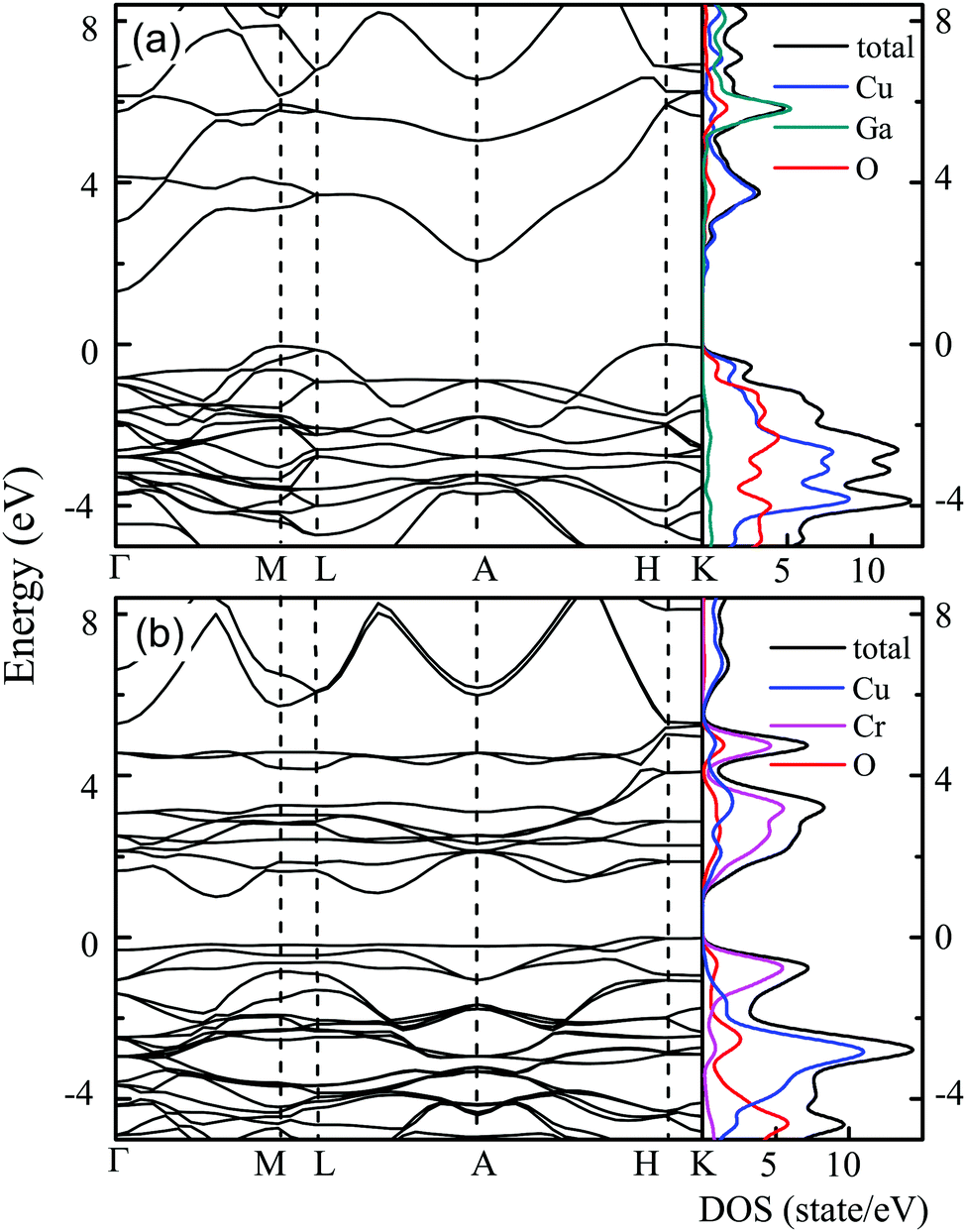 | ||
| Fig. 1 Calculated electronic band structure and density of states for (a) CuGaO2 and (b) CuCrO2. | ||
In Fig. 1(b), the band structure for CuCrO2 is visibly different to that for CuGaO2. The band structure also exhibits an indirect band gap, whereas the direct gap is found near M in the direction of Γ. The qualitative positions of the fundamental transition are in good agreement with the consequence reported by David O. Scanlon et al.,12 who also used a hexagonal polymorph and GGA to simulate the case of CuCrO2. For CuCrO2, there is an experimentally demonstrated redshift in the optical absorption relative to the CuGaO2 structure.20 From further research into the electronic densities of states, the reason for the extended band structure feature for CuCrO2 becomes apparent. The DOS of CuCrO2 suggests a significant number of states at the Fermi level, which are dominated by Cr orbitals. The Cr states and the Cu states can be hybridized with each other via O states in the CuCrO2 structure.21,27 In addition, the Cu states from −2 to −4 eV for CuGaO2 are less pronounced and present a higher main peak located at −3 eV for CuCrO2. The VBM is dominated by the Cr states, whereas the more dispersed Cu states are pushed to lower energies relative to the VBM, leading to a flat valence band. Similarly, the bottom of the conduction band is predominantly contributed by the Cr states both with some Cu and O states, causing the flattening of the CBM.
Fig. 2 shows the band structure of CuGa0.5Cr0.5O2 for both α-spin and β-spin, respectively. Obviously, the band structure for the α-spin channel has a strong resemblance to that for CuCrO2 in Fig. 1(b). However, the band gap for the β-spin is also nearly the same as that for CuGaO2 in Fig. 1(a). This phenomenon can be found in the (Fe/Cr)2O3 system, which can be ascribed to the strong localization of the Cr states.28 Moreover, the calculated band gap is indirect and the value is unchanged from the CuGaO2 structure. However, the CBM for both spins is located at Γ, no longer near M for the CuCrO2 structure. The VBM is present just off H along H–A and the VBM for the α-spin is higher than that for the β-spin. This variation indicates that the valence band level position can be raised by Cr-doping, thus decreasing the optical transition energy.
 | ||
| Fig. 2 Calculated electronic band structure of CuGa0.5Cr0.5O2 for (a) α-spin and (b) β-spin. | ||
The PDOSs of the CuGa0.5Cr0.5O2 structure for both α-spin and β-spin components are shown in Fig. 3. Based on the introduction of Cr into the Ga lattice sites in alternating ab layers, the oxygen atoms are divided into two categories: O1 and O2. The O1 pattern is located between Cu and Ga, while the O2 one makes a connection with Cu and Cr. Interestingly, the O1 2p state in Fig. 3(e) is similar to the DOS of O for the CuGaO2 structure. From Fig. 3(f), a lager shoulder at −0.5 eV for the α-spin component is increased due to the O2–Cr interaction. Beyond that, the O2 2p state is spin polarized, which is affected by the formed stable bond with spin polarized Cr ions. It demonstrates that the local O coordination environment is only dependent on the peculiarity of the directly contacted atoms. Moreover, the Cr3+ (3d3) ionic charge state has a multiple-electron energy-level structure. The approximately octahedral crystal field can reduce orbital degeneracy and split three d electrons into the occupied t2g state and the empty eg state.29,30 As a consequence, three occupied single electron Cr 3d states migrate to the top of the valence band, as shown in Fig. 3(d). The unoccupied α-spin Cr 3d states, eg, constitute the conduction band bottom, whereas the β-spin band states, t2g, migrate to the high energy of the conduction band.22,31 This effect is assigned to the ferromagnetic ground state.32
 | ||
| Fig. 3 The electronic density of states for CuGa0.5Cr0.5O2. (a) Total PDOS, (b) Cu 3d, (c) Ga 4s, (d) Cr 3d, (e) and (f) O 2p. | ||
Moreover, copper (Cu) contributes less to the top of the valence band compared to the CuGaO2 structure. On the contrary, oxygen O2 in particular, occupies more states in the CBM and VBM. The Ga atoms are unable to produce this effect. The difference in chemical bonding between CuGaO2 and CuCrO2 is responsible for the significant deviation of the band structure and density of states. For CGCOx, the longer Cr–O bonds generate strain on the lattice. A stronger covalent interaction between Cr 3d and O 2p and an indirect Cr 3d–Cu 3d hybridized interaction occur.33 Hence, the partial charge from O2 shifts to Cr and the charge transfer from O2 to Cu decreases. Beyond that, the Cr 3d states dominate at the top of the valence band and the bottom of the conduction band is enhanced significantly with increasing Cr composition. This results in a weakening of the Cu 3d + O 2p → Cu 3dz2 + 4s transition. Moreover, the states in the Cu–O–Cr–O–Cu linkages should be mixed effectively by heavy doping, which further moves the valence band upwards and the conduction band downwards, thus resulting in a lower optical band gap.
3.2 Structure and surface analysis
Fig. 4(a) shows the XRD patterns of the CGCOx films with different Cr concentrations. All samples were measured using a glancing angle configuration to eliminate the contribution of the substrate. It can be found that all films are polycrystalline with a stronger (012) diffraction peak, which locates at about 36.4°. Furthermore, the intensity of (012) peaks enhanced with the increase in the Ga constituent. Besides the strong feature, several other weaker diffraction peaks (006), (104), (105), (110) were observed. Note that the variation trend of the (006) peak with composition x is abnormal, which may be attributed to the polycrystalline growth. Taking the standard XRD pattern of CuGaO2 (JCPDS card No. 41-0255) into consideration, all of the films show a pure rhombohedral phase structure. No impurity phase is observed in the films except for the CGCO0 film, indicating that the Cr atoms have been successfully incorporated into the CGCOx host lattice. Fig. 4(b) shows the supercell of the CGCOx rhombohedral structure. Note that each Cu atom is linearly coordinated between two oxygen atoms, forming O–Cu–O dumbbells along the c axis, which agrees well with the main peak of the XRD patterns.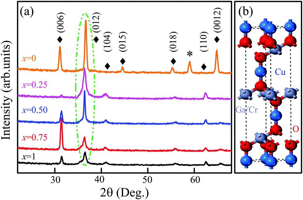 | ||
| Fig. 4 (a) XRD patterns of the CGCOx films grown on (001) sapphire substrates. The symbol (*) indicates the observed trace of the sapphire substrate. (b) The rhombohedral unit cell of the delafossite structure. | ||
Fig. 5(a) and (e) show the three-dimensional AFM images of the CGCO0.25 and CGCO1 films, respectively. The film grains are closely gathered and densely arranged, which indicates that all the films exhibit nanocrystalline growth. The root-mean-square (RMS) surface roughness is estimated to be 6.39, 4.56, 6.73, 12.8, and 16.7 nm for the Cr concentration at x = 0, 0.25, 0.5, 0.75, and 1, respectively. It can be seen that the RMS surface roughness decreased first, and increased with increasing Cr-composition. The grain size change shows a similar variation trend, which is attributed to the effect induced by Cr-substitution. It indicates that the crystal quality was increased by light doping, whereas the heavy doping resulted in more crystal defects. Scanning electron microscopy (SEM) is another common technique for investigating the morphology of the films. Cross-sectional SEM can be applied to measure the thickness of the films. The plane-view SEM images of the CGCOx films are shown in Fig. 5(b)–(d), (f) and (g), respectively. Note that the grain size is homogeneous and varied with the change in Cr-composition. The particle gaps decreased first, and increased with increasing Cr-composition. In addition, the CGCO0.25 film has the smallest gaps, which agrees well with the RMS surface roughness. The remarkable variation in surface morphology can affect the optical and electrical properties, such as lattice vibrations and electronic transitions. In the cross-sectional image, an obvious interface between the film and sapphire substrate can be observed and the thickness of the CGCO0.25 film is about 240 ± 10 nm.
 | ||
| Fig. 5 Three-dimensional AFM images of (a) CGCO0.25 and (e) CGCO1 films. Note that the different scale heights are given in the pictures and the measured area is 1 × 1 μm2. The plane-view SEM images of (b) CGCO0, (c) CGCO0.25, (d) CGCO0.5, (f) CGCO0.75 and (g) CGCO1 films. The picture (h) shows the cross-sectional image of the CGCO0.25 film. Note that the same scale is given in the picture. | ||
3.3 Chemical bond and valence states
In order to understand the molecular structure, chemical bond and valence states of the CGCOx films, XPS and infrared reflectance spectra were obtained. The IR spectra of the CGCOx films recorded at room temperature are shown in Fig. 6. As we know, the primitive rhombohedral unit cell of delafossite compounds contains four atoms, giving rise to 12 normal modes.34,35 Group-theoretical analysis decomposes a general mode at the Brillouin zone center Γ as = A1g + Eg + 3A2u + 3Eu. Eu and A2u symmetries are infrared active and include acoustic modes, in which both oxygens must move in the phase.36 In Fig. 6(a), the observed infrared active modes near 502 cm−1 and 733 cm−1 of the CGCO1 film can be inferred to the E↑u and A↑2u vibrations, respectively. For the CGCO0 film, the A↑2u mode is found clearly at 655 cm−1. The E↑u mode around 500 cm−1 is too weak to be discovered, which agrees well with previous studies.36 The displacement patterns of the E↑u and A↑2u at the Brillouin zone center are shown in the inset of Fig. 6(a). It is no wonder that the vibration is related to the O–Cu–O–M units. | ||
| Fig. 6 (a) Infrared reflectance spectra of the CGCOx films at room temperature. The dashed lines show the vibration trend of the phonon modes. (b) An enlarged reflectance spectra region between 485 and 545 cm−1. (c) IR spectra of the CGCO films in the range of 636–800 cm−1. | ||
Interestingly, the intensity of the E↑u peaks for the CGCOx films becomes stronger with increasing x, as shown in Fig. 6(b). However, the peak position is almost unchanged. For the A↑2u phonon mode the peak position shifts from 655 cm−1 to 733 cm−1 obviously [Fig. 6(c)]. The O–Cu–O bond is seriously affected by the substitution of Ga with Cr, which can be ascribed to the lower Cr mass and stiffer Cr–O bonds. The double degenerate E mode expresses movement in the perpendicular direction relative to the c-axis. However, the A mode describes the vibration in the direction of the O–Cu–O bonds along the hexagonal c-axis. Therefore, the E↑u mode frequency increment is not as pronounced as that of the A↑2u mode.37 This indicates that a structural transition stimulated by Cr-doping would not modify the octahedral environment of the Ga atoms. Nevertheless, the element Cu may reduce the site symmetry for the Cr–O–Cu–O units.
As an example, Fig. 7(a) displays the overall core level XPS survey spectra of the CGCO0.5 film. The intense peaks of Cu 2p, Cr 2p, Ga 3d and O 1s can be observed. The C 1s peak at 284.6 eV is used as an internal standard to correct the binding energy position of other elements. Fig. 7(b–e) show the Lorentzian–Gaussian dividing peak analysis of the Cu 2p, O 1s, Cr 2p and Ga 3d peaks, respectively. In Fig. 7(b), the 1/2 and 3/2 spin–orbit doublet components of the Cu 2p photoelectron are found to be located at about 952.4 eV and 932.2 eV for the CGCO0.5 film, respectively.34 Note that there is no shake-up line of Cu 2p3/2 in the spectra. This indicates that the valence of the Cu ions is +1 in the present CGCOx films. The O 1s peak is deconvoluted into two individual peaks [Fig. 7(c)]. The lower binding energy peak located at about 530 eV is attributed to the lattice oxygen, whereas the higher binding energy peak positioned at about 532 eV should be attributed to the surface adsorbed hydroxyl oxygen. In Fig. 7(d), the Cr 2p peaks at binding energies of 576.9 and 586.8 eV for the CGCO1 film can be assigned to Cr 2p3/2 and Cr 2p1/2 peaks, respectively. The Ga 3d peaks at binding energies of 20.6 eV (Ga 3d5/2) and 22.7 eV (Ga 3d3/2) for the CGCO0 film can be found in Fig. 7(e). The XPS data suggest that both Cr and Ga ions possess +3 valence states.
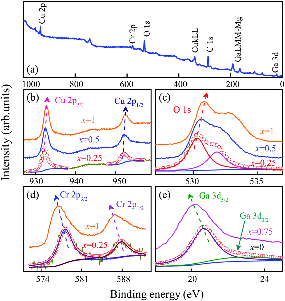 | ||
| Fig. 7 (a) Overall core level XPS spectra of the CGCO0.5 film. XPS spectra of the Cu 2p (b), O 1s (c), Cr 2p (d) and Ga 3d (e) regions for the CCGOx films. Note that the dotted lines represent the nonlinear fitting results. | ||
It is well known that the binding energy is closely related to the chemical environment of the atoms. The combination of different element types and quantities will change the binding energy of inner shell electrons. It can be seen that the peak positions of Cu 2p and O 1s show a blueshift, whereas the peak positions of Cr 2p and Ga 3d show a redshift with increasing Cr composition. This means that the microstructure of the CGCOx film can be changed by Cr-substitution, which is attributed to the hybridization of Cr 3d states with O 2p energy levels. This indicates that an indirect Cr–Cu interaction is modified by the Cu–O–Cr bond, which agrees well with the above theoretical calculations. Moreover, the Cu–O and Ga–O bonds for CGCOx structures can be affected by the shorter Cr–O bond. The Ga–O distance becomes longer, whereas the Cu–O (Cr) length decreases. Therefore, the binding energy of Cu 2p and O 1s is enhanced, while the Ga 3d related core levels are decreased by Cr-doping.
3.4 Optical transitions
Fig. 8(a) shows the transmittance spectra for the CGCOx films at room temperature. It can be clearly seen that each film has a relatively high optical transmittance in the visible range. Note that the CGCO1 film has a mild absorption edge, whereas the CGCO0 film has the steepest absorption edge, which can be attributed to the introduction of the Cr element. The absorption edge for the CGCOx films shows a redshift trend with increasing Cr composition, which is assigned to the hybridization of Cr 3d states and O 2p states from the first-principles calculations. However, an abnormal absorption edge appears for the CGCO0.25 film. This indicates that there are two electronic transitions in this region. The transmittance spectra of the CGCO0.25 film at different temperatures are plotted in Fig. 8(b). The enlarged transmittance spectra from 10 K to 300 K for the CGCO0.25 and CGCO0.5 films near the absorption edge are shown in Fig. 8(c) and (d), respectively. Anomalously, the absorption edge for the CGCO0.25 film shows a blueshift trend with increasing temperature at low temperatures and the largest absorption edge appears at about 125 K. However, the absorption edge for the CGCO0.5 film shows a redshift trend with increasing temperature, which is also found in other films (not shown).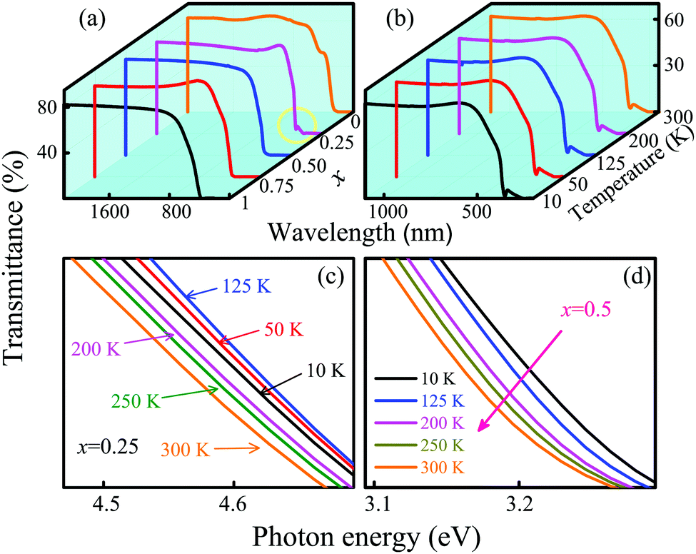 | ||
| Fig. 8 (a) Transmittance spectra of the CGCOx films at room temperature. The yellow circle shows an abnormal absorption. (b) Transmittance spectra of the CGCO0.25 film at different temperatures. An enlarged spectral region near the absorption edge for CGCO0.25 (c), and CGCO0.5 (d) at different temperatures. | ||
In order to understand the temperature dependence of the band-gap behavior in detail, the optical band gap energies were investigated. The optical band gap, named EOBG, is deduced by Tauc's relationship (αhν)n = A(hν − EOBG). The EOBG can be estimated by an intercept of the (αhν)n plot.38α denotes the absorption coefficient, which can be obtained using the relationship: α = −ln(T)/d. T, d and A are the transmittance of the films, the thickness and a constant, respectively. The exponent n determines the type of optical transitions, with n = 2 for a direct band gap (EdirOBG) and 1/2 for an indirect band gap (EindirOBG) transition, respectively.
For the CGCO0.5 film, the EdirOBG can be estimated to be 3.20 eV at 10 K and 3.13 eV at 300 K, while the EindirOBG is 2.86 eV and 2.79 eV, respectively [Fig. 9(a) and (b)]. In Fig. 1, it can be seen that both Cu 3d and O 2p states contribute to the upper part of the valence band and the bottom of the conduction band for CuGaO2. In particular, the CBM is mainly dominated by the Cu 3dz2 and 4s characters.12,24 However, it can be found that the near-Fermi-level structure is primarily dominated by Cr 3d states in the structure which has both Cu and Cr elements, as shown in Fig. 3. Thus, the direct electronic transition of the CGCO0.5 film can be ascribed to the excitation of the 3d → 3d transition, which is attributed to the covalent interaction between Cr 3d and O 2p orbitals.22 It is worth noting that the optical band gap shows a redshift with increasing temperature for both direct and indirect electronic transitions, which is attributed to the lattice thermal expansion and the electron–phonon interaction.39 The distance between the lattices gradually increases with temperature and the lattice wave frequency changes with the crystal volume.40,41 Moreover, the valence band bottom represents an upward movement as the electrons of the semiconductor are energized, resulting in the modification of the electronic band structure.
 | ||
| Fig. 9 (a) Plots of (αhν)2vs. the photon energy for the estimation of direct optical band gap energies from the CGCO0.5 film. The inset shows the electronic transition diagram. (b) Plots of (αhν)1/2vs. the photon energy for the estimation of indirect band gap energies from the CGCO0.5 film. (c) An enlarged region for the indirect band gap. | ||
Next we turn our attention to the abnormal absorption edge of the CGCO0.25 film. The characteristic is only observed for 0 < x ≤ 0.3 and the absorption becomes weaker with the increasing composition of Cr. To investigate the origin of this extraordinary phenomenon, the temperature dependence of the EdirOBG for the CGCO0.25 film has been plotted in Fig. 10(a). It is worth noting that there are two interband transitions, named Eg1 and Eg2, respectively. The Eg1 transition corresponds to the strong absorption and can be estimated to be 3.31 eV at 300 K, which is slightly higher than the EdirOBG of the CGCO0.5 film. As shown in Fig. 8(a), the strong absorption for CGCOx films can be modified by Cr doping, which indicates that the strong absorption corresponds to the essential optical feature. Therefore, the Eg1 energy band is attributed to the 3d → 3d transition from the valence-band maximum (VBM) to the conduction-band minimum (CBM) after introducing the Cr element [Fig. 10(c)].42,43 In Fig. 10(d), the Eg1 band gap shows a redshift trend with increasing temperature. However, it can be observed that the band gap energy decreases with temperature in the low temperature region, whereas the variation is much less than that from 150 K to 300 K from Fig. 10(e), which can be attributed to the lattice thermal expansion. With increasing temperature, the interatomic distance along the direction of the propagation can be changed by the longitudinal phonons and the lattice thermal expansion becomes stronger.40 Note that these mechanisms become increasingly important with the temperature, in order to increase the variation rate of the band gap.
 | ||
| Fig. 10 (a) Plots of (αhν)2vs. the photon energy for the determinations of direct optical band gap energies from the CGCO0.25 film. (b) Temperature dependence of the Eg2 energy band. (c) Electronic transitions diagram for the CGCO0.25 film. (d) An enlarged region for the Eg1 transition. (e) Temperature dependence of the Eg1 energy band. | ||
The Eg2 transition can be ascribed to the absorption edge region. At room temperature, the energy band Eg2 at about 3.61 eV can be found, which agrees well with the band gap of CGCO0 in the previous reports.44 Note that the band structure of delafossites will be modified by M-site alloying, while the essential optical features remain unchanged for light doping. The retention of the direct band gap for CGCO0 after alloying can be expected based on similar findings in the predicted band structure CuGa1−xFexO2.45 Therefore, the Eg2 transition may be ascribed to the dipole-allowed Cu 3d + O 2p → Cu 3dz2 + 4s transition [Fig. 10(c)],22,46 which corresponds to the L–L transition in Fig. 1(a).
More remarkably, the Eg2 energy band shows a non-monotonic trend with increasing temperature [Fig. 10(b)]. The minimum band-gap energy appears at the highest temperature of 300 K, whereas the maximum energy appears at about 125 K, instead of the lowest temperature of 10 K. This anomalous temperature behavior was also observed in other materials with monovalent Cu or Ag cations, such as Cu(Cr/Mg)O2 and AgGaSe2.41,47 All these materials possess a maximum gap energy at a relatively low temperature. Note that the anomalous temperature variation in the low temperature region is related to p–d electron hybridization.48 The p–d hybridization will be further enhanced by the occupied Cr 3d states interacting covalently with the neighboring O 2p states, which makes the abnormal phenomenon much clearer.49 Extraordinarily, the Eg2 energy band can become weaker by increasing the Cr doping composition, which is attributed to the stronger interaction Cr 3d–O 2p–Cu 3d.41 Measurements at low temperatures using crystals with pairwise replacement of isotopes would help to separate the individual effects of the various atoms on the zero-temperature gap renormalization.
4 Conclusion
In summary, the electronic structure of the CGCOx system was investigated theoretically using first-principles calculations and temperature-dependent transmittance spectroscopy for the first time. It can be found that the relevant electronic transitions calculated using the exchange–correlation potential of the GGA type in the PBE version agree well with the experimental data for the CGCOx films. Replacing Ga with Cr results in the appearance of Cr 3d states. The Cr–O interaction indirectly changes the Cu–O bonds, which causes an increase in the density of 3d states at the top of the valence band and the bottom of the conduction band. In addition, the vibration frequency of infrared active phonon modes and the binding energy of Cu 2p and O 1s increase with Cr composition due to the lower Cr mass and stiffer Cr–O bonds. Moreover, the abnormal absorption in CGCO0.25 is attributed to the Cu 3d + O 2p → Cu 3dz2 + 4s transition. The non-monotonic trend of the Eg2 transition in the low temperature region is attributed to the covalent interaction Cr 3d–O 2p–Cu 3d and should become weaker with more Cr-doping. Remarkably, the spin–orbit interactions of the Cr3+ ions in an octahedral environment increase the density of states at the CBM and VBM for CGCOx (0 < x ≤ 1). Therefore, the optical absorption edge is dominated by the excitation of the 3d → 3d transition. This can bring out the overlap of 3d states, thus increasing the mobility of p-type charge carriers.Acknowledgements
This work was financially supported by the Major State Basic Research Development Program of China (Grant No. 2013CB922300), the Natural and Science Foundation of China (Grant No. 11374097, 61376129 and 61504156), the Projects of Science and Technology Commission of Shanghai Municipality (Grant No. 15JC1401600 and 14XD1401500), and the Program for Professor of Special Appointment (Eastern Scholar) at Shanghai Institutions of Higher Learning.References
- C. T. Liu, Y. C. Wang, R. X. Dong, C. C. Wang, K. C. Huang, R. Vittal, K. C. Ho and J. J. Lin, J. Mater. Chem., 2012, 22, 25311–25315 RSC.
- J. Y. Kim, J. H. Jeon and M. K. Kwon, ACS Appl. Mater. Interfaces, 2015, 7, 7945–7950 CAS.
- A. C. Tamboli, M. F. A. M. van Hest, M. A. Steiner, S. Essig, E. E. Perl, A. G. Norman, N. Bosco and P. Stradins, Appl. Phys. Lett., 2015, 106, 263904 CrossRef.
- Y. M. Kim, W. J. Lee, D. R. Jung, J. M. Kim, S. H. Nam, H. C. Kim and B. W. Park, Appl. Phys. Lett., 2010, 96, 171902 CrossRef.
- W. J. Ong, L. L. Tan, S. P. Chai, S. T. Yonga and A. R. Mohamed, Nanoscale, 2014, 6, 1946–2008 RSC.
- C. Tong, J. Y. Yun, Y. J. Chen, D. X. Ji, Q. Q. Gan and W. A. Anderson, ACS Appl. Mater. Interfaces, 2016, 8, 3985–3991 CAS.
- A. Kudo, H. Yanagi, H. Hosono and H. Kawazoe, Appl. Phys. Lett., 1998, 73, 220–222 CrossRef CAS.
- J. Roberston, R. Gillen and F. Villuendas, Phys. Rev. B: Condens. Matter Mater. Phys., 2012, 85, 125306 CrossRef.
- S. Sheng, G. Fang, C. Li, S. Xu and X. Zhao, Phys. Status Solidi A, 2006, 203, 1891–1900 CrossRef CAS.
- H. Kawazoe, M. Yasukawa, H. Hyodo, M. Kurita, H. Yanagi and H. Hosono, Nature, 1997, 389, 939 CrossRef CAS.
- K. Ueda, T. Hase, H. Yanagi, H. Kawazoe, H. Hosono, H. Ohta, M. Orita and M. Hirano, J. Appl. Phys., 2001, 89, 1790–1793 CrossRef CAS.
- D. O. Scanlon and G. W. Watson, J. Mater. Chem., 2011, 21, 3655–3663 RSC.
- J. Gu, Y. Yan, J. W. Krizan, Q. D. Gibson, Z. M. Detweiler, R. J. Cava and A. B. Bocarsly, J. Am. Chem. Soc., 2014, 136, 830–833 CrossRef CAS PubMed.
- J. Gu, A. Wuttig, J. W. Krizan, Y. Hu, Z. M. Detweiler, R. J. Cava and A. B. Bocarsly, J. Phys. Chem. C, 2013, 117, 12415–12422 CAS.
- Z. Xu, D. H. Xiong, H. Wang, W. J. Zhang, X. W. Zeng, L. Q. Ming, W. Chen, X. B. Xu, J. Cui, M. K. Wang, S. Powar, U. Bach and Y. B. Cheng, J. Mater. Chem. A, 2014, 2, 2968–2976 CAS.
- J. Wang, V. Ibarra, D. Barrera, L. Xu, Y. J. Lee and J. W. P. Hsu, J. Phys. Chem. Lett., 2015, 6, 1071–1075 CrossRef CAS PubMed.
- J. Wang, Y. J. Lee and J. W. P. Hsu, J. Mater. Chem. C, 2016, 4, 3607–3613 RSC.
- A. K. D. Garc, T. L. Villarreal and R. Gomez, J. Mater. Chem. A, 2015, 3, 19683–19687 Search PubMed.
- A. Renaud, L. Cario, P. Deniard, E. Gautron, X. Rocquefelte, Y. Pellegrin, E. Blart, F. Odobel and S. Jobic, J. Phys. Chem. C, 2014, 118, 54–59 CAS.
- M. J. Han, K. Jiang, J. Z. Zhang, W. L. Yu, Y. W. Li, Z. G. Hu and J. H. Chu, J. Mater. Chem., 2012, 22, 18463–18470 RSC.
- T. Yokobori, M. Okawa, K. Konishi, R. Takei, K. Katayama, S. Oozono, T. Shinmura, T. Okuda, H. Wadati, E. Sakai, K. Ono, H. Kumigashira, M. Oshima, T. Sugiyama, E. Ikenaga, N. Hamada and T. Saitoh, Phys. Rev. B: Condens. Matter Mater. Phys., 2013, 87, 195124 CrossRef.
- R. Gillen and J. Robertson, Phys. Rev. B: Condens. Matter Mater. Phys., 2011, 84, 035125 CrossRef.
- I. Suzuki, H. Nagatani, M. Kita, Y. Iguchi, C. Sato, H. Yanagi, N. Ohashi and T. Omata, Inorg. Chem., 2016, 55, 7610–7616 CrossRef CAS PubMed.
- M. N. Huda, Y. Yan, A. Walsh, S. H. Wei and M. M. Al-Jassim, Phys. Rev. B: Condens. Matter Mater. Phys., 2009, 82, 035205 CrossRef.
- J. P. Perdew, K. Burke and M. Ernzerhof, Phys. Rev. Lett., 1996, 77, 3865–3868 CrossRef CAS PubMed.
- A. Buljan, M. Llunell, E. Ruiz and P. Alemany, Chem. Mater., 2001, 13, 338–344 CrossRef CAS.
- D. O. Scanlon, A. Walsh, B. J. Morgan and G. W. Watson, Phys. Rev. B: Condens. Matter Mater. Phys., 2009, 79, 035101 CrossRef.
- M. N. Huda, A. Walsh, Y. F. Yan, S. H. Wei and M. M. Al-Jassim, J. Appl. Phys., 2010, 107, 123712 CrossRef.
- D. L. Wood, J. Ferguson, K. Knox and J. F. Dillon Jr., J. Chem. Phys., 1963, 39, 890–898 CrossRef CAS.
- M. Schmidt, Z. Wang, Ch. Kant, F. Mayr, S. Toth, A. T. M. N. Islam, B. Lake, V. Tsurkan, A. Loidl and J. Deisenhofer, Phys. Rev. B: Condens. Matter Mater. Phys., 2013, 87, 224424 CrossRef.
- H. Hiraga, T. Makino, T. Fukumura, H. M. Weng and M. Kawasaki, Phys. Rev. B: Condens. Matter Mater. Phys., 2011, 84, 041411 CrossRef.
- S. Blugel, M. Weinert and P. H. Dederichs, Phys. Rev. Lett., 1988, 60, 1077–1080 CrossRef PubMed.
- D. Shin, J. S. Foord, R. G. Egdell and A. Walsh, J. Appl. Phys., 2012, 112, 113718 CrossRef.
- S. P. Pavunny, A. Kumar and R. S. Katiyar, J. Appl. Phys., 2010, 107, 013522 CrossRef.
- X. R. Li, J. Y. Wang, J. Z. Zhang, Y. W. Li, Z. G. Hu and J. H. Chu, RSC Adv., 2016, 6, 27136–27142 RSC.
- J. P. Porres, A. Segura, E. Martnez, A. M. Saitta, A. Polian, J. C. Chervin and B. Canny, Phys. Rev. B: Condens. Matter Mater. Phys., 2005, 72, 064301 CrossRef.
- J. P. Porres, D. M. Garca, A. Segura, P. R. Hernandez, A. Muñoz, J. C. Chervin, N. Garro and D. Kim, Phys. Rev. B: Condens. Matter Mater. Phys., 2006, 74, 184301 CrossRef.
- J. Tauc, R. Gigorovici and A. Vancu, Phys. Status Solidi, 1966, 15, 627–637 CrossRef CAS.
- M. Cardona and M. L. W. Thewalt, Rev. Mod. Phys., 2005, 77, 1173–1223 CrossRef CAS.
- S. Biernacki, U. Scherz and B. K. Meyer, Phys. Rev. B: Condens. Matter Mater. Phys., 1994, 49, 4501–4510 CrossRef CAS.
- J. Bhosale, A. K. Ramdas, A. Burger, A. Muñoz, A. H. Romero, M. Cardona, R. Lauck and R. K. Kremer, Phys. Rev. B: Condens. Matter Mater. Phys., 2012, 86, 195208 CrossRef.
- W. T. Lim, L. Stafford, P. W. Sadik, D. P. Norton, S. J. Pearton, Y. L. Wang and F. Ren, Appl. Phys. Lett., 2007, 90, 142101 CrossRef.
- D. O. Scanlon, K. G. Godinho, B. J. Morgan and G. W. Watson, J. Chem. Phys., 2010, 132, 024707 CrossRef PubMed.
- S. Gilliland, J. P. Porres, A. Segura, A. Muñoz, P. R. Hernañdez, D. Kim, M. S. Lee and T. Y. Kim, Phys. Status Solidi B, 2007, 244, 309–314 CrossRef CAS.
- J. W. Lekse, M. K. Underwood, J. P. Lewis and C. Matranga, J. Phys. Chem. C, 2012, 116, 1865–1872 CAS.
- X. L. Nie, S. H. Wei and S. B. Zhang, Phys. Rev. Lett., 2002, 88, 066405 CrossRef PubMed.
- J. Serrano, Ch. Schweitzer, C. T. Lin, K. Reimann, M. Cardona and D. Fröhlich, Phys. Rev. B: Condens. Matter Mater. Phys., 2002, 65, 125110 CrossRef.
- S. Levcenco, S. Doka, V. Tezlevan, D. F. Marron, L. Kulyuk, T. S. Niedrig, M. Ch. L. Steinerb and E. Arushanov, Physica B, 2010, 405, 3547–3550 CrossRef CAS.
- X. R. Li, M. J. Han, X. L. Zhang, C. Shan, Z. G. Hu, Z. Q. Zhu and J. H. Chu, Phys. Rev. B: Condens. Matter Mater. Phys., 2014, 90, 035308 CrossRef.
| This journal is © The Royal Society of Chemistry 2017 |