
Solution-processed electron-only tandem polymer light-emitting diodes for broad wavelength light emission†
Sung Hwan
Cho
a,
Eui Hyuk
Kim
a,
Beomjin
Jeong
a,
Ju Han
Lee
a,
Giyoung
Song
a,
Ihn
Hwang
a,
Himchan
Cho
b,
Kang Lib
Kim
a,
Seunggun
Yu
a,
Richard Hahnkee
Kim
a,
Seung Won
Lee
a,
Tae-Woo
Lee
b and
Cheolmin
Park
*a
aDepartment of Materials Science and Engineering, Yonsei University, Seoul 120-749, Republic of Korea. E-mail: cmpark@yonsei.ac.kr
bDepartment of Materials Science and Engineering, Pohang University of Science and Technology (POSTECH), Pohang 790-784, Republic of Korea
First published on 21st November 2016
Abstract
Polymer light-emitting diodes (PLEDs) have been of great interest for flexible mobile displays and large area solid-state lighting due to the possibility of achieving low production costs using solution processes combined with various printing technologies. Although monochromatic operation of PLEDs with high luminous efficiency and device stability has been achieved using numerous strategies, the development of color-tunable PLEDs capable of emitting a broad range of light upon the application of external stimuli still remains challenging. Here, we present a solution-processed broad range color-tunable tandem PLED of inverted and regular light emitting units (LEUs) stacked in series sharing a floating polymer electrode as a charge injection layer between two LEUs. Fine and broad wavelength color control from pure blue to pure orange is achieved when an AC field is applied with different positive-to-negative polarity heights in our tandem PLED. Our AC-driven tandem PLEDs offer a facile route to color-tunable polymer EL devices with a maximum current efficiency (CE) and luminance of 2.5 cd A−1 and 1300 cd m−2 for blue emission under DC reverse and 6.7 cd A−1 and 6000 cd m−2 for orange emission under DC forward as well as 3.1 cd A−1 and 6000 cd m−2 for white emission under AC, respectively.
Introduction
Polymer light-emitting diodes (PLEDs) have attracted considerable interest for flexible mobile displays and large-area solid-state lighting since they can be produced inexpensively using solution processes combined with various printing technologies.1,2 Although monochromic operation of PLEDs with high luminous efficiency and device stability has been achieved using numerous strategies,3–18 the development of color-tunable PLEDs capable of emitting a broad range of light in response to external stimuli remains a challenge. The majority of previous studies attempting to address this challenge have involved the development of color-tunable organic light-emitting diodes (OLEDs) having small-molecule-based layers. These studies can be categorized into two main approaches: (1) color-tunable single OLEDs19–25 and (2) color-tunable tandem OLEDs, wherein individually operating color units are stacked with each other.26–30 The color of single OLEDs has been controlled on the basis of the shift of the emission peak, which is dependent upon the applied voltage. This peak-position shift arises as a function of voltage because of the efficient energy transfer from the host to the dopant luminescent material,19 the control of the relative brightness of the host and dopant materials,20 and the shift of the recombination zone using blocking layers21,22 in multiple emission layers. Color tuning has been achieved via control of the voltage polarity direction between the top and bottom electrodes.23–25 Furthermore, color-tunable single PLEDs have also been developed using similar principles.31–34 These types of devices, however, show a limited tuning range, which hardly covers the full emission spectrum of pure red, green, and blue.An alternative route for facile color control is based on tandem OLEDs, which have allowed fine color control over a broad range of emission wavelengths.26–30 A tandem OLED having two stacked regular device units sharing a thin and transparent Ag/Au electrode has been developed; this three-terminal device exhibits excellent color tunability, depending upon the positive-to-negative voltage ratio in its alternating current (AC) voltage input.29 In addition, an AC-driven electron-only tandem OLED in which two regular and inverted units are stacked in series with a thin transition metal oxide film as a field-induced charge injection layer inserted between the two units has been demonstrated.30 In spite of the usefulness of a tandem architecture for the broad wavelength emission control, only a few tandem PLEDs have been reported with solution-processed constituent layers.
Here, we demonstrate broad wavelength color-tunable tandem PLEDs based on an AC-driven device architecture of vertically stacked inverted and regular light-emitting units (LEUs). All 7 constituent layers except the top and bottom electrodes of our tandem PLED were fabricated by spin-coating, including the hole- and electron-transport, emission, and highly conductive PEDOT:PSS charge injection layers. Fine and broad wavelength color control from pure blue to pure orange was achieved when an AC field was applied with different positive-to-negative polarity heights in our tandem PLED consisting of an inverted and a regular unit with a blue and an orange light-emitting layer, respectively. Color control from pure blue to pure red was also readily achieved when the orange-emitting layer was replaced by a red-emitting layer. With the optimization of the fabrication and device operation conditions, our AC-driven tandem PLEDs with PEDOT:PSS charge injection layers offer a facile route for color-tunable polymer EL devices with a maximum current efficiency (CE) and luminance of 2.5 cd A−1 and 1300 cd m−2 for blue emission under DC reverse and 6.7 cd A−1 and 6000 cd m−2 for orange emission under DC forward and 3.1 cd A−1 and 6000 cd m−2 for white emission under AC, respectively.
Experimental
Materials
A blue poly(spirobifluorene)-based copolymer (product SPB-02T), a red poly(spirobifluorene)-based copolymer (product SPR-001), and super orange (product PDO-134) were purchased from Merck Co. AI4083 PEDOT:PSS (Clevios P VP AI4083) was modified by mixing equal ratios of isopropyl alcohol with 0.6 wt% Zonyl surfactant (FS-300 fluorosurfactant from Aldrich) for promoting the wetting of an emission layer.35 High-conductivity PEDOT:PSS (Clevios PH1000) was also modified by mixing with 6 wt% of dimethyl sulfoxide (DMSO)36 and 0.5 wt% Zonyl surfactant12,35 with respect to PEDOT:PSS. All other materials were purchased from Aldrich and were used as received.Fabrication of tandem PLEDs
The device architecture of tandem PLEDs is illustrated in Fig. 1a. First, the ITO substrate (80 nm, 30 Ω cm−2) was sequentially cleaned twice with acetone and 2-propanol for 15 min each and then with UV light for 15 min. Zinc acetylacetonate hydrate (Zn(acac)2, Sigma-Aldrich) was dissolved in anhydrous ethanol (25 mg mL−1) and stirred at 50 °C for 24 h.7,12 A ZnO precursor solution filtered through a PTFE filter (0.45 μm) was spin-coated onto cleaned ITO-coated glass, followed by thermal annealing in air at 120 °C for 30 s, leading to the formation of a 10 nm-thick ZnO film. Subsequently, 0.4 wt% PEI dissolved in 2-methoxyethanol was spin-coated onto the ZnO film and the approximately 10 nm-thick PEI film was annealed at 100 °C for 10 min in air.6–8,12 For layer deposition, the bottom blue-emissive film was prepared by spin-coating a solution dissolved in toluene (1.2 wt%) onto PEI/ZnO layers. The AI4083 layer was then spin-coated from the modified solution, as previously described.35 After an annealing process at 120 °C for 5 min, the f-PH1000 layer was spin-coated from a modified PH1000 solution, and then annealed at 120 °C for 5 min. For the top LEU deposition process, a modified AI4083 layer was spin-coated and then annealed at 120 °C for 5 min, and the top orange emissive films were deposited by spin-coating solutions dissolved in toluene (0.5 wt%) onto the modified AI4083 layer. Afterward, a LiF/Al layer (1 and 120 nm) was deposited under a pressure of 10−6 mbar. The devices were encapsulated in glass with a moisture getter film (Dynic HD-071313W-48) using UV-curable epoxy resin (Nagase XNR5570) in a glove box and the size of the active area was 0.4 cm2.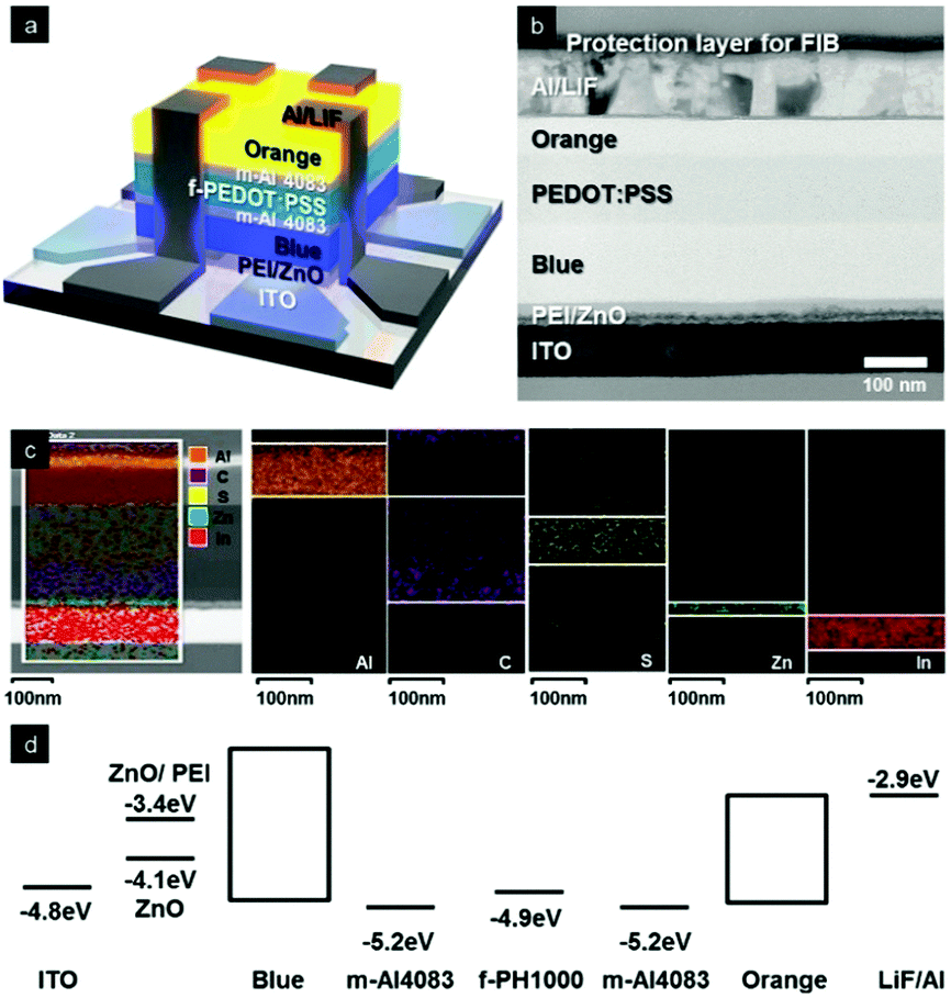 | ||
| Fig. 1 (a) Schematic of a broad-range wavelength-tunable tandem PLED. (b) High-resolution cross-sectional TEM image of the tandem PLED. Scale bar is 100 nm. (c) TEM-EDX measurements with multivariate statistical analysis of characteristic atomic elements of the constituent layers. Scale bar is 100 nm. (d) The energy levels of the color-tunable tandem PLED device. | ||
Characterization
The surface of the constituent layers was analyzed using tapping-mode AFM (Nanoscope Iva, Digital Instruments) with height and phase contrast. The multi-layered tandem PLED structures were analyzed using a focused-ion-beam transmission electron microscope (FIBTEM) (JIB-4601F, JEOL) and a spherical aberration correction scanning transmission electron microscope (STEM) (JEOL JEM-ARM 200F). The time-of-flight secondary ion mass spectrometry (ToF-SIMS) depth profile was analyzed using a TOF SIMS5 instrument (ION-TOF GmbH, Munster, Germany) with a 30 keV Bi1+ beam for analysis and a 0.5 keV Cs+ beam for sputtering. The examined area was 100 × 100 μm2. The optical absorption was obtained from a Perkin-Elmer Lambda 750 UV-Vis spectrophotometer. The luminance and EL spectra of devices were obtained using a spectroradiometer (Konica CS 2000). The current–voltage–luminance (I–V–L) characteristics of the devices were measured with a multichannel precision power analyzer under AC (ZIMMER Electronics Systems LMG 500) and with a source measurement unit under DC (Keithley 2400) coupled with the spectroradiometer. All measurements were performed in a dark box under ambient conditions in air.Results and discussion
We fabricated a blue-to-orange color-tunable tandem PLED with vertically stacked multi-layers of ITO/zinc oxide (ZnO)/polyethyleneimine (PEI)/BLUE/modified-AI4083 PEDOT:PSS (hereafter denoted as m-AI4083)/high-conductivity PH1000 PEDOT:PSS/m-AI4083/ORANGE/LiF/Al from bottom to top. Our electron-only tandem PLED includes a bottom inverted LEU stacked with a top regular LEU sharing a common floating PEDOT:PSS electrode (hereafter denoted as f-PH1000), as illustrated in Fig. 1a. ZnO/PEI and LiF were used as electron injection layers from ITO to blue and Al to orange, respectively, whereas m-AI4083 layers treated with the Zonyl surfactant35 on both sides of f-PH1000 were used as hole injection layers from f-PH1000 to bottom blue and top orange layers (Fig. 1d). A PEI layer was introduced to reduce the injection barrier between ZnO and blue because of its strong dipole moment.6–8 The multi-layers of our tandem PLED developed by successive spin-coating processes were evidenced by cross-sectional high-resolution transmission electron microscopy (TEM) images collected simultaneously with two-dimensional energy-dispersive X-ray spectrometry (2D EDX) measurements, as shown in Fig. 1b and c. The bright-field TEM results in Fig. 1b clearly show an approximately 10 nm-thick ZnO layer followed by the ∼10 nm PEI, ∼100 nm blue, ∼90 nm PEDOT:PSS, and ∼50 nm orange layers and the LiF/Al top electrode. 2D EDX maps of specific atomic elements of the constituent layers (Fig. 1c) confirm the formation of the discrete layers. In particular, m-AI4083/f-PH1000/m-AI4083 PEDOT:PSS layers have sharp interfaces without mixing between active and PEDOT:PSS layers and effectively protect the underlying bottom LEU from the solvents used for fabricating the top LEU (ESI,† Fig. S1).The surface morphology of each layer was also analyzed upon fabrication by atomic force microscopy (AFM); the results show that all of the layers exhibit very low root-mean-squared (RMS) roughness, which indicates that no damage occurred during the successive spin-coating of layers as shown in Fig. 2a–h.10,11 To confirm the minimal damage to the blue emitting layer underneath m-AI4083/f-PH1000/m-AI4083 upon deposition of the orange emitting layer spin-coated from a solution in toluene, we on purpose spread toluene on a m-AI4083/f-PH1000/m-AI4083/blue emitting layer and examined the optical properties of the blue emitting layer. UV-vis absorption results in Fig. 2i show that intensities of UV-vis absorption were not significantly altered after rinsing in toluene, which indicates that m-AI4083/f-PH1000/m-AI4083 trilayers are sufficiently resistive to toluene, giving rise to the successful protection of the underlying blue emitting layer.
 | ||
| Fig. 2 (a) The surface morphology of each layer of a tandem PLED analyzed by AFM indicated very low RMS roughness of (a) ITO (1.839 nm), (b) ZnO (2.061 nm), (c) PEI (1.322 nm), (d) blue (0.658 nm), (e) AI4083 (1.168 nm), (f) PH1000 (3.275 nm), (g) AI4083 (1.822 nm), and (h) orange (1.333 nm). The height scale is 30 nm and scale bar is 50 nm. (i) UV-vis absorption spectra of the pristine and toluene rinsed structures consisting of vertically stacked multi-layers of ITO/zinc oxide (ZnO)/polyethyleneimine (PEI)/BLUE/m-AI4083/high-conductivity PH1000 PEDOT:PSS/m-AI4083. | ||
In order to further confirm the discrete multi-layer stacking with negligible intermixing of the constituent layers in our tandem PLED, we analyzed the depth profile using ToF-SIMS (ESI,† Fig. S2). We monitored Al−, C−, S−, ZnO− and In− ion signals corresponding to the Al top electrode, emissive materials, PEDOT:PSS, ZnO and the ITO bottom electrode, respectively. The results show an Al− signal from the Al electrode followed by C− signals which represent three sharp peak intensities from the blue emissive layer, PEDOT:PSS layer and orange emissive layer. The signal intensity of the S− ion was also observed from the PEDOT:PSS charge injection layer, followed by a carbon signal for the blue emissive layer. Finally, ZnO− and In− signals were observed, arising from ZnO and ITO layers. The discrete ion signals in the mass spectra from ToF-SIMS indicate that damage or intermixing rarely occurred during the successive spin-coating of the multi-layers.
The operation mechanism of our tandem PLEDs is schematically depicted in Fig. 3. When a direct current (DC) forward bias is applied to the top Al and bottom ITO electrodes (the first scheme in Fig. 3a), electrons are injected from the top electrode to the orange layer; simultaneously, field-induced holes are injected from the highly conductive f-PH1000 to the orange layer. The excitons subsequently formed in the upper emissive layer recombine radiatively, giving rise to light emission from the top LEU. No light is emitted from the bottom inverted LEU because of the high hole-injection barrier between the ZnO/PEI and a blue fluorescent polymer layer and the high electron-injection barrier between a blue fluorescent polymer layer and the m-AI4083 layer (Fig. 1d).6,7 In contrast, under reverse DC bias, the bottom inverted LEU emits light because of the facile injection of electrons from ITO to ZnO/PEI, whereas no emission occurs from the top LEU, as shown in Fig. 3b. The application of an AC field with sequentially alternating voltage polarity to our tandem PLED can thus be a useful method to operate both LEUs alternately; moreover, at a sufficiently high frequency, two lights from the LEUs are efficiently mixed with each other, as schematically shown in Fig. 3c. More importantly, because the brightness of an LEU increases with the applied voltage, the application of an AC field with different polarity heights of positive and negative voltages allows for further control of the maximum wavelength of a mixed emission light from the peak wavelength of an emission layer of the top LEU to that of the bottom LEU, giving rise to a broad-wavelength-tunable tandem PLED.
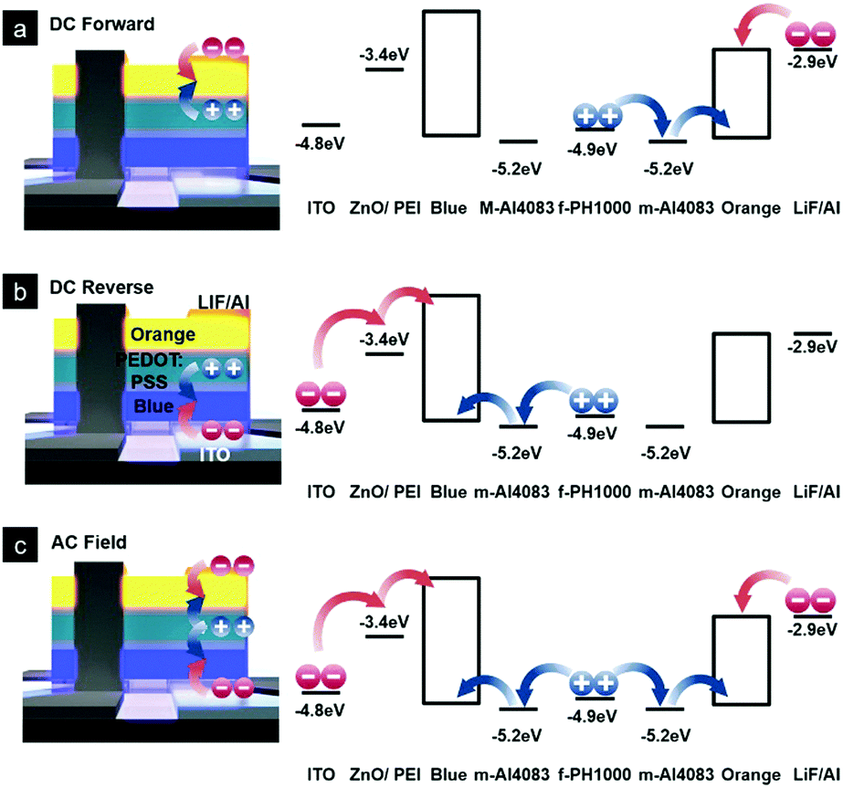 | ||
| Fig. 3 The operation mechanism of top orange and bottom blue tandem PLEDs coupled with energy-level alignment under (a) DC forward, (b) DC reverse and (c) AC fields. | ||
Either blue or orange light was successfully radiated at reverse or forward DC bias, respectively, as evidenced in Fig. 4a. When an AC field with a frequency of 500 Hz was applied, our tandem PLED emitted white light arising from the color mixing of blue and orange, as shown in the EL spectrum in Fig. 4a. The Commission Internationale de l'Enclairage (CIE) coordinates of the device further confirm the effective control of emission color by the application of DC and AC fields; the coordinates are (0.1647, 0.2659), (0.5121, 0.4850), and (0.3256, 0.3809) for reverse DC, forward DC, and AC fields, respectively, which correspond to typical blue, orange, and white emission, as shown in Fig. 4b. The photographs on the right hand side of Fig. 4b clearly show blue, orange and white light emission of a tandem PLED developed with reverse DC, forward DC, and AC fields, respectively.
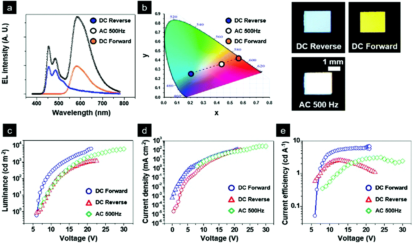 | ||
| Fig. 4 (a) EL spectra and (b) CIE coordinates of a tandem PLED with top orange and bottom blue LEUs under reverse DC, forward DC, and AC biases. Photographs of the device taken under DC and AC fields are also shown on the right hand side. Scale bar is 1mm. (c) Luminance versus voltage characteristics (L–V), (d) current density versus voltage characteristics (J–V), and (e) CE versus voltage characteristics of a tandem PLED with top orange and bottom blue LEUs under reverse and forward DC and AC biases. | ||
The detailed light-emitting performance of our tandem PLED was investigated in terms of luminance (L), current density (J), and CE as a function of applied voltage under reverse and forward DC biases as well as under an applied AC field; the results are shown in Fig. 4c–e, respectively. Under both DC and AC biases, the device exhibited similar luminance versus voltage (L–V) behavior, as shown in Fig. 4c. The maximum brightness of the device was approximately 6000 cd m−2 at 30 V and 500 Hz; we obtained a similar brightness under a forward DC bias, even at a lower voltage of 21 V. The bottom LEU may show its performance worse than that of the top LEU because of the higher electron injection barrier of the bottom LEU from ITO for the DC reverse bias than that of the top LEU from LiF/Al for the DC forward bias. However, it is not easy to clearly observe the effect of the injection barrier mentioned above in our tandem device which has two emission layers with different light emission efficiencies.
A single regular PLED device composed of ITO/AI4083/Orange/LiF/Al and a single inverted PLED device composed of ITO/ZnO/PEI/Blue/m-AI4083/Al were also investigated for comparison in terms of luminance (L), current density (J), and CE versus DC reverse voltages (ESI,† Fig. S3). A single orange regular PLED device has 60![[thin space (1/6-em)]](https://www.rsc.org/images/entities/char_2009.gif) 000 cd m−2 and 8 cd A−1 of maximum brightness and current efficiency, whereas a single blue inverted PLED device has 2500 cd m−2 and 2.8 cd A−1 of maximum brightness and current efficiency. The current density results shown in Fig. 4d indicate that the top LEU has higher current density at forward DC than that of bottom LEU at reverse DC. This result has similar current density tendency of single regular and inverted PLED devices. As expected, the AC-driven tandem PLED exhibits current density versus voltage (J–V) behavior that is intermediate between the behaviors of the two DC-driven devices. At below threshold voltage, the tandem PLED showed low leakage current under reverse and forward DC bias. A device operated under AC may be more stable than one under DC due to reduced charge accumulation in the interface. It is noted that a single regular PLED device composed of ITO/AI4083/Orange/LiF/Al showed the breakdown voltage under AC bias higher than that under DC bias.
000 cd m−2 and 8 cd A−1 of maximum brightness and current efficiency, whereas a single blue inverted PLED device has 2500 cd m−2 and 2.8 cd A−1 of maximum brightness and current efficiency. The current density results shown in Fig. 4d indicate that the top LEU has higher current density at forward DC than that of bottom LEU at reverse DC. This result has similar current density tendency of single regular and inverted PLED devices. As expected, the AC-driven tandem PLED exhibits current density versus voltage (J–V) behavior that is intermediate between the behaviors of the two DC-driven devices. At below threshold voltage, the tandem PLED showed low leakage current under reverse and forward DC bias. A device operated under AC may be more stable than one under DC due to reduced charge accumulation in the interface. It is noted that a single regular PLED device composed of ITO/AI4083/Orange/LiF/Al showed the breakdown voltage under AC bias higher than that under DC bias.
The top LEU under forward DC bias exhibits a maximum CE of approximately 6.7 cd A−1, whereas the bottom LEU under reverse DC bias and the device operated under AC bias exhibit maximum CEs of approximately 2.5 and 3.1 cd A−1, respectively, as shown in Fig. 4e. We also obtained power efficiency of our tandem PLEDs with a maximum power efficiency of 1.3, 1.1 and 0.6 lm W−1 under DC forward, reverse and AC biases, respectively (ESI,† Fig. S4). Our results are considerable in particular considering that a recent electron-only color-tunable OLED with 14 vacuum deposited constituent layers exhibited its maximum CE and brightness of approximately 2 cd A−1 and 1300 cd m−2, respectively.30Table 1 summarizes the bias-dependent performance of our tandem PLED, along with the detailed device parameters.
| Voltage polarity | V on | CRI | V [V] at 100/1000/6000 cd m−2 | Current efficiency (cd A−1) at 100/1000/6000 cd m−2 | Maximum CE (cd A−1) |
|---|---|---|---|---|---|
| Forward bias | 6.5 | 78 | 9/13.5/20.7 V | 3.1/5.4/6.7 cd A−1 | 6.7 cd A−1 At 6100 cd m−1 |
| Reverse bias | 7 | 33 | 12/20.5/NA V | 2.5/1.4/NA cd A−1 | 2.5 cd A−1 At 150 cd m−2 |
| AC bias | 6.5 | 47 | 12/17/30 V | 0.96/2.2/2.4 cd A−1 | 3.1 cd A−1 At 3400 cd m−1 |
We also examined the AC-frequency-dependent device performance; the results in Fig. 5a show that our device is insensitive to frequency in the range from 100 to 1000 Hz. Above 1 kHz, however, the tandem PLED became frequency-dependent and the luminance drastically decreased with the frequency in the range from 1 kHz to 1000 kHz. The electron injection from top and bottom electrodes upon application of the AC field was limited due to too fast polarity switching at high frequency, giving rise to the low luminescence. The capacitance change of a tandem PLED as a function of applied voltage supports our claim as shown in Fig. 5b. The capacitance value of our tandem PLED measured at the frequency below 1 kHz decreases smoothly as the applied voltage increases. At higher voltage and at 500 Hz, for instance, the capacitance even became negative. The negative capacitance behavior at a low frequency has been reported previously for PLEDs, attributed to efficient carrier injection from the electrode to the emissive layer.37,38 As noted, at a frequency above 1 kHz, a tandem PLED shows the capacitance independent of the applied voltage, which indicates that the carrier injection was hampered by emissive layers, due to limited carrier mobility under a fast bias polarity switching speed. We confirmed that the negative capacitance in a low frequency regime was also observed in a conventional regular device (ESI,† Fig. S5).
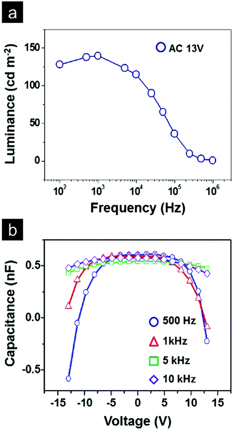 | ||
| Fig. 5 (a) Luminance versus frequency characteristics of the tandem PLEDs at AC ±13 V. (b) Capacitance versus voltage characteristics of the blue/orange tandem PLED as a function of frequency. | ||
To investigate the field induced charge injection mechanism from f-PH1000 to LEUs without external circuit connection, we fabricated a capacitor type PLED with an insulating SiO2 layer. The device consists of ITO/SiO2/f-PH1000PEDOT:PSS/m-AI4083/ORANGE/LiF/Al from bottom to top, as shown in Fig. 6a. The proposed energy level of the device in Fig. 6b indicates that electrons from the LiF/Al electrode can be easily injected into the emission layer while holes cannot be injected from ITO into the emission layer due to the 200 nm thick SiO2 insulator inserted between an emitting layer and the ITO electrode. In this situation, the plenty of internal excess charges in the conductive f-PEDOT:PSS layer can allow for facile hole injection induced by the electric field into the emission layer, giving rise to light emission upon recombination of excitons. As expected, the device was turned on when both DC and AC were applied. Luminance (cd m−2) as a function of voltage (V) of the PLED with a SiO2 insulator was very similar to that of a PLED without an insulator (a regular PLED device) as shown in Fig. 6c. The maximum brightness of the device was approximately 20000 cd m−2 under both AC and DC biases. Interestingly, in spite of a 200 nm thick insulator, the device shows its current density 3 times lower than that of a regular PLED without an insulator as shown in Fig. 6d (ESI,† Fig. S3). The results clearly demonstrate that the f-PH1000 electrode is able to effectively inject charges (holes) into an emission layer. The device exhibits the maximum CE of approximately 10 cd A−1 at 10000 cd m−2 under DC and approximately 8 cd A−1 at 10000 cd m−2 under AC bias, respectively, as shown in Fig. 6e. A regular PLED without an insulator is shown in Fig. 6d. It should be noted that no light was emitted from a device with an insulator when the f-PH1000 electrode was removed, which implies that our f-PH1000 electrode between an insulator and an active layer successfully acts as a field induced charge injection layer. The results also suggest that a f-PH1000 electrode in our color-tunable tandem PLED efficiently allows for the field induced hole injection into an emission layer under either an AC or a DC field.
 | ||
| Fig. 6 (a) Schematic of a capacitor type PLED with an insulator. (b) The energy level diagram of the capacitor type PLED. (c) Luminance versus voltage characteristics (L–V), (d) current density versus voltage characteristics (J–V), and (e) CE versus voltage characteristics of the capacitor type PLED under forward DC as well as AC biases. | ||
The dynamic switching response of the tandem PLED was investigated as an applied voltage train to confirm that both top and bottom LEUs function properly over time. The time-resolved current density (mA cm−2) versus the applied voltage (V) measurement of the tandem PLED in Fig. 7a indicates that as the AC ΔV of the symmetric voltage train with the same positive (forward) and negative (reverse) values increases, the corresponding current densities with positive and negative values gradually increase; this result indicates that the top and bottom LEUs accordingly respond at the voltage bias. Under an AC field with a sufficiently high voltage of ±20 V, the ON current density value of each LEU was well maintained over time (ESI,† Fig. S6). An inverted or a regular PLED, however, functions only at reverse or forward voltage bias, respectively. For instance, an inverted PLED with a blue-emission layer exhibited only current density at a negative voltage bias, whereas no current was detected at positive voltage inputs, as shown in Fig. 7b. A constant current density was observed only at each input of +10 V of AC ΔV of ±10 V (ESI,† Fig. S7).
 | ||
| Fig. 7 Time-resolved current density of (a) a tandem PLED with top orange and bottom blue LEUs and (b) an inverted PLED with a blue-emission layer as a function of the AC ΔV inputs with symmetric positive and negative voltages. (c) Time-resolved EL of the tandem PLED at different frequencies (top). EL signals at 460 and 580 nm were monitored for top orange and bottom blue LEUs repeatedly with an AC ΔV input of ±14 V; time-resolved EL signals of an inverted PLED with a blue-emission layer as a function of frequency with an AC ΔV input of ±10 V are shown in the bottom. | ||
Time-resolved electroluminescence (EL) experiments as a function of frequency also support the independent operation of both LEUs of tandem PLEDs at positive and negative voltage biases, as shown in Fig. 7c and Fig. S8a–d (ESI†). In tandem PLEDs, orange-light emission was observed upon the application of a positive voltage, whereas blue emission occurred when a negative voltage was applied. Notably, however, an inverted PLED functions only at a negative polarity at all frequencies, resulting in light flickering, especially at frequencies lower than 50 Hz39–41 (ESI,† Fig. S7).
In contrast, light emission from our tandem PLED under both voltage polarities allowed the device to remain ON upon successive voltage trains, which can avoid light flickering, even at very low frequencies. By carefully adjusting the relative height of the positive and negative voltages used to control the emission intensity of orange and blue light, respectively, we substantially reduced flickering over a wide frequency range from 1 Hz to 1 kHz (ESI,† Fig. S8). The voltage-polarity-dependent light emission of the top and bottom LEUs as well as the effective color mixing of the two emitting lights under an AC field in our tandem PLED provide a facile route for controlling the position of the maximum wavelength of emitted light at frequencies greater than approximately 50 Hz AC frequency which is fast enough for the human eye not to distinguish the blue and orange emissions from bottom and top LEUs, respectively29 due to fast polarity change (cf. demonstration in the ESI,† Movie S1).
We achieved fine color tuning from pure blue to pure orange in our tandem PLED by varying the voltage heights of positive and negative polarities of the AC field, as shown in Fig. 8a. Five EL spectra with different wavelengths at the maximum intensity were representatively demonstrated at different positive/negative AC voltage heights ranging from +2/−16 to +16/−6 at the AC frequency of 100 Hz. A broader color tuning from pure blue to pure red was also demonstrated with a tandem PLED composed of an inverted blue LEU stacked with a regular red LEU; the results clearly show that the EL spectra with different wavelengths at the maximum intensity were obtained by controlling the AC voltage height of the positive and negative inputs, as shown in Fig. 8b (ESI,† Fig. S9). The fractions of either blue or orange color determined by comparing the maximum peak intensity with respect to that of each pure color were linearly controlled by adjusting the heights of both positive and negative AC voltages, as shown in Fig. 8c. A similar linear variation of either blue or red color was also demonstrated in a tandem PLED with blue- and red-emission layers in Fig. 8d. These results suggest that fine-tuning of a mixed color can be readily achieved by simply adjusting the two voltage values of the AC inputs. To demonstrate the finer color tuning capability of our tandem PLED, we applied more subdivided AC voltage inputs; the results, reported in Fig. 8e (see also ESI,† Fig. S10 and S11), show that broad wavelength color control is indeed achievable.
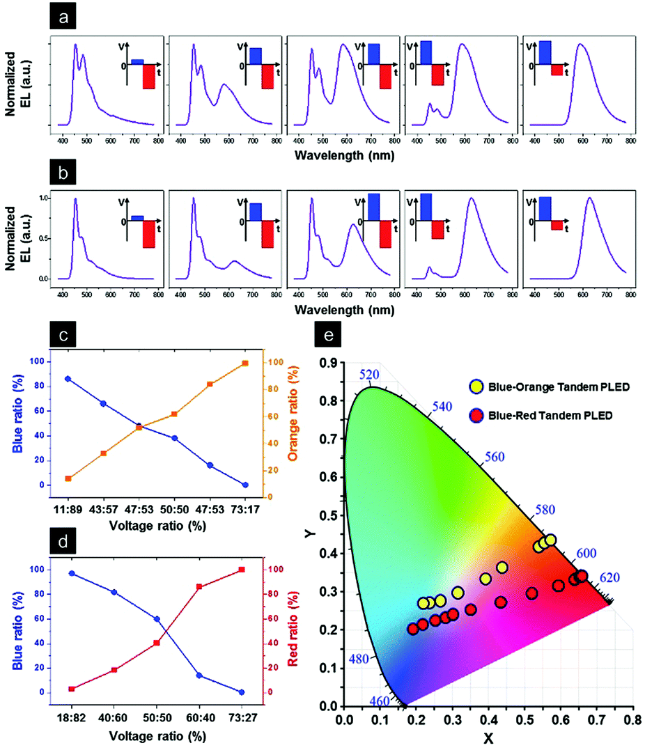 | ||
| Fig. 8 (a) EL spectra of a tandem PLED with bottom blue and top orange LEUs operated under an AC bias with asymmetric positive and negative voltage heights of +2:−16 V, +12:−16 V, +14:−16 V, +16:−14 V, and +16:−6 V. (b) EL spectra of a tandem PLED with top red and bottom blue LEUs operated under an AC bias with asymmetric positive and negative voltage heights of +4:−18 V, +12:−18 V, +18:−18 V, +18:−12 V, and +18:−6 V. A plot of the intensity fractions of (c) blue/orange and (d) blue/red in normalized EL spectra of bottom blue/top orange and bottom blue/top red tandem PLEDs operated at different AC biases. (e) CIE coordinates corresponding to the EL spectra of the top orange/bottom blue and top red-bottom blue tandem PLEDs under 8 and 12 AC voltage forms with different positive and negative heights at the AC frequency of 100 Hz. | ||
Conclusions
In summary, we developed a solution-processed electron-only tandem PLED wherein a regular LEU was stacked on an inverted LEU with a field-induced PEDOT:PSS charge injection layer. Independent operation of the top and bottom LEUs was achieved at reverse and forward DC biases, respectively. An AC field applied to the device allowed for repetitive turn-on of the top and bottom LEUs at the corresponding voltage bias, thereby reducing the flickering frequently observed with such devices under AC operation. The frequency dependent luminance of our tandem PLED further elucidated the operation principle of the device. Furthermore, by adjusting the positive and negative input voltage heights of the AC field in a tandem PLED with different top and bottom emission layers, we achieved facile and fine color tuning via efficient mixing of the top and bottom emission colors. This work clearly demonstrates that broad wavelength color-tunable PLEDs were realized from pure blue to pure red under novel AC operation. Our device platform based on solution processes offers a simple but robust route for low-cost and broad range color tunable displays.Acknowledgements
This research was supported by DAPA, ADD and the third stage of the Brain Korea 21 Plus project in 2014 and by a grant from the National Research Foundation of Korea (NRF), funded by Korean government (MEST) (No. 2014R1A2A1A01005046).Notes and references
- J. H. Burroughes, D. D. C. Bradley, A. R. Brown, R. N. Marks, K. Mackay, R. H. Friend, P. L. Burns and A. B. Holmes, Nature, 1990, 347, 539–541 CrossRef CAS.
- S. Shin, M. Yang, L. J. Guo and H. Youn, Small, 2013, 9, 4036–4044 CrossRef CAS PubMed.
- R. H. Friend, R. W. Gymer, A. B. Holmes, J. H. Burroughes, R. N. Marks, C. Taliani, D. D. C. Bradley, D. A. Dos Santos, J. L. Bredas, M. Lögdlund and W. R. Salaneck, Nature, 1999, 397, 121–128 CrossRef CAS.
- M. T. Bernius, M. Inbasekaran, J. O'Brien and W. S. Wu, Adv. Mater., 2000, 12, 1737–1750 CrossRef CAS.
- H. Nakanotani, T. Higuchi, T. Furukawa, K. Masui, K. Morimoto, M. Numata, H. Tanaka, Y. Sagara, T. Yasuda and C. Adachi, Nat. Commun., 2014, 5, 4016 CAS.
- Y.-H. Kim, T.-H. Han, H. Cho, S.-Y. Min, C.-L. Lee and T.-W. Lee, Adv. Funct. Mater., 2014, 24, 3808–3814 CrossRef CAS.
- S. Hofle, A. Schienle, C. Bernhard, M. Bruns, U. Lemmer and A. Colsmann, Adv. Mater., 2014, 26, 2750–2754 CrossRef PubMed.
- Y. Zhou, C. F-Hernandez, J. Shim, J. Meyer, A. J. Giordano, H. Li, P. Winget, T. Papadopoulos, H. Cheun, J. Kim, M. Fenoll, A. Dindar, W. Haske, E. Najafabadi, T. M. Khan, H. Sojoudi, S. Barlow, S. Graham, J. Brédas, S. R. Marder, A. Kahn and B. Kippelen, Science, 2012, 336, 327–332 CrossRef CAS PubMed.
- T. Chiba, Y.-J. Pu, H. Sasabe, J. Kido and Y. Yang, J. Mater. Chem., 2012, 22, 22769–22773 RSC.
- Y.-J. Pu, T. Chiba, K. Ideta, S. Takahashi, N. Aizawa, T. Hikichi and J. Kido, Adv. Mater., 2015, 27, 1327–1332 CrossRef CAS PubMed.
- T. Chiba, Y.-J. Pu and J. Kido, Adv. Mater., 2015, 27, 4681–4687 CrossRef CAS PubMed.
- S. Höfle, A. Schienle, C. Bernhard, M. Bruns, U. Lemmer and A. Colsmann, Adv. Mater., 2014, 26, 5155–5159 CrossRef PubMed.
- S. Höfle, C. Bernhard, M. Bruns, C. Kübel, T. Scherer, U. Lemmer and A. Colsmann, ACS Appl. Mater. Interfaces, 2015, 7, 8132–8137 Search PubMed.
- Y. Chen, G. M. Smith, E. Loughman, Y. Li, W. Nie and D. L. Carroll, Org. Electron., 2013, 14, 8–18 CrossRef CAS.
- Y. Chen, Y. Xia, H. Sun, G. M. Smith, D. Yang, D. Ma and D. L. Carroll, Adv. Funct. Mater., 2014, 24, 1501–1508 CrossRef CAS.
- Y. Chen, Y. Xia, G. M. Smith, H. Sun, D. Yang, D. Ma, T. Li, W. Huang and D. L. Carroll, Adv. Funct. Mater., 2014, 24, 2677–2688 CrossRef CAS.
- Y. Xia, Y. Chen, G. M. Smith, Y. Li, W. Huang and D. L. Carroll, Appl. Phys. Lett., 2013, 102, 253302 CrossRef.
- Y. Chen, Y. Xia, G. M. Smith and D. L. Carroll, Adv. Mater., 2014, 26, 8133–8140 CrossRef CAS PubMed.
- G. Cheng, K. T. Chan, W.-P. To and C.-M. Che, Adv. Mater., 2014, 26, 2540–2546 CrossRef CAS PubMed.
- W. X. Li, J. Hagen, R. Jones, J. Heikenfeld and A. J. Steckl, Solid-State Electron., 2007, 51, 500–504 CrossRef CAS.
- W. C. H. Choy, J. H. Niu, X.-W. Chen, W. L. Li and P. C. Chui, Appl. Phys. A: Mater. Sci. Process., 2007, 89, 667–671 CrossRef CAS.
- J.-H. Jou, M.-H. Wu, S.-M. Shen, H.-C. Wang, S.-Z. Chen, S.-H. Chen, C.-R. Lin and Y.-L. Hsieh, Appl. Phys. Lett., 2009, 95, 013307 CrossRef.
- Y. Z. Wang, R. G. Sun, D. K. Wang, T. M. Swager and A. J. Epstein, Appl. Phys. Lett., 1999, 74, 2595 Search PubMed.
- M. Yoshida, A. Fujii, Y. Ohmori and K. Yoshino, Appl. Phys. Lett., 1996, 69, 734–736 CrossRef CAS.
- M. Hamaguchi, A. Fujii, Y. Ohmori and K. Yoshino, Jpn. J. Appl. Phys., 1996, 35, 397–400 CrossRef.
- Z. Shen, P. E. Burrows, V. Bulović, S. R. Forrest and M. E. Thompson, Science, 1997, 276, 2009–2011 CrossRef CAS.
- G. Parthasarathy, G. Gu and S. R. Forrest, Adv. Mater., 1999, 11, 907–910 CrossRef CAS.
- P. E. Burrows, S. R. Forrest, S. P. Sibley and M. E. Thompson, Appl. Phys. Lett., 1996, 69, 2959–2961 CrossRef CAS.
- M. Fröbel, T. Schwab, M. Kliem, S. Hofmann, K. Leo and M. C. Gather, Light: Sci. Appl., 2015, 4, e247 CrossRef.
- Y. Zhao, R. Chen, Y. Gao, K. S. Leck, X. Yang, S. Liu, A. P. Abiyasa, Y. Divayana, E. Mutlugun, S. T. Tan, H. Sun, H. V. Demir and X. W. Sun, Org. Electron., 2013, 14, 3195–3200 CrossRef CAS.
- M. Berggren, O. Inganäs, G. Gustafsson, J. Rasmusson, M. R. Andersson, T. Hjertberg and O. Wennerström, Nature, 1994, 372, 444–446 CrossRef CAS.
- M. Granström and O. Inganäs, Appl. Phys. Lett., 1996, 68, 147–149 CrossRef.
- M. C. Gather, R. Alle, H. Becker and K. Meerholz, Adv. Mater., 2007, 19, 4460–4465 CrossRef CAS.
- Y. Yang and Q. Pei, Appl. Phys. Lett., 1996, 68, 2708–2710 CrossRef CAS.
- C. Y. Chang, L. Zuo, H. L. Yip, Y. Li, C. Z. Li, C. S. Hsu, Y. J. Cheng, H. Chen and A. K. Y. Jen, Adv. Funct. Mater., 2013, 23, 5084–5090 CrossRef CAS.
- S.-I. Na, G. Wang, S.-S. Kim, T.-W. Kim, S.-H. Oh, B.-K. Yu, T. Lee and D.-Y. Kim, J. Mater. Chem., 2009, 19, 9045–9053 RSC.
- L. S. C. Pingree, B. J. Scott, M. T. Russell, T. J. Marks and M. C. Hersam, Appl. Phys. Lett., 2005, 86, 073509 CrossRef.
- K. Bansal, Phys. Status Solidi C, 2013, 10, 593–596 CrossRef CAS.
- T. Nobeshima, T. Morimoto, K. Nakamura and N. Kobayashi, J. Mater. Chem., 2010, 20, 10630–10633 RSC.
- H.-H. Yen, W.-Y. Yeh and H.-C. Kuo, Phys. Status Solidi A, 2007, 204, 2077–2081 CrossRef CAS.
- H. Lin, B. Wang, J. Xu, R. Zhang, H. Chen, Y. Yu and Y. Wang, ACS Appl. Mater. Interfaces, 2014, 6, 21264–21269 CAS.
Footnote |
| † Electronic supplementary information (ESI) available: Optical and electrical characteristic results. See DOI: 10.1039/c6tc04229e |
| This journal is © The Royal Society of Chemistry 2017 |