A two-dimensional tetragonal yttrium nitride monolayer: a ferroelastic semiconductor with switchable anisotropic properties
Bo
Xu
 *ab,
Hui
Xiang
b,
Jiang
Yin
*bc,
Yidong
Xia
bc and
Zhiguo
Liu
bc
aSchool of Sciences, Key Laboratory of Biomedical Functional Materials, China Pharmaceutical University, Nanjing 211198, China. E-mail: xubonju@gmail.com
bNational Laboratory of Solid State Microstructures and Department of Materials Science and Engineering, College of Engineering and Applied Sciences, Nanjing University, Nanjing 210093, China. E-mail: jyin@nju.edu.cn
cCollaborative Innovation Center of Advanced Microstructures, Nanjing University, Nanjing, 210093, China
First published on 22nd November 2017
Abstract
We propose a two-dimensional (2D) tetragonal material: an yttrium nitride (t-YN) monolayer, with a distinguished combination of mechanical and electronic properties based on first-principles calculations. We find that the t-YN monolayer is a low direct band gap semiconductor (0.55 eV) with strong anisotropic mechanical and electronic properties. We also identify that the t-YN monolayer to be a 2D ferroelastic material with a reversible strain of about 14.4%, indicating that the anisotropic properties of the t-YN monolayer can be switched by applying external stress. Furthermore, the moderate-switching barrier (33 meV/atom) of ferroelastic lattice rotation renders the switchable anisotropic properties accessible experimentally. These outstanding properties make the t-YN monolayer a promising switchable anisotropic 2D material for electronic and mechanical applications.
1. Introduction
The successful isolation of graphene in 20041 led us into the new world of two-dimensional (2D) materials. The family of 2D materials with a rich variety of electronic properties2–10 has attracted considerable research interest. Most 2D materials, such as graphene,1 transition metal dichalcogenides2–4 (MX2, where M denotes a transition metal and X denotes a chalcogen), C3N4,5 and BN,6 exhibit isotropic behaviors along with their lattice structures and symmetries.Being different from isotropic 2D materials, several anisotropic 2D materials have been reported and have attracted considerable attention.11–17 For example, the anisotropic structures of mono- and few-layer black phosphorus11 give rise to a significant in-plane anisotropy in electron and hole masses, as well as in carrier mobility, Young's modulus, and optical properties. Monochalcogenides, such as GeSe and SnSe,18 with phosphorene-like structures, also show strong in-plane anisotropy in electronic, optical and spin–orbital coupling. Liu et al.19 demonstrated that monolayer ReS2 with a distorted 1T structure exhibits anisotropic carrier mobilities along the two principal axes. Unlike these anisotropic semiconductors, 2D boron sheet (borophane)20 was predicted to be a highly anisotropic metal, and Mannix et al.21 confirmed this by using scanning tunneling spectroscopy. Zhou et al.22 also reported that 2D orthorhombic (Pmmn) boron was an anisotropic semimetal with the presence of a Dirac cone. Recently, a new kind of anisotropic material, a 2D tetragonal TiC monolayer, has been proposed.23 Due to the tetragonal symmetry, the TiC monolayer shows anisotropy in mechanical and electronic properties. The line of research has been extended to other 2D anisotropic tetragonal-structured metal nitride (MN, M = Ti, Zr, Hf, Nb, Cr)24–27 monolayers as well. These unique anisotropic behaviors can be used to identify 2D materials and to design conceptually novel devices in experiments. These anisotropic properties of 2D materials can be further manipulated by applying an external field, especially strain engineering, which has been widely used to tune the properties of 2D materials. For example, Fei et al.14 proposed that the anisotropic free-carrier mobility of phosphorene can be controlled by strain engineering.
Furthermore, if the anisotropic properties, including the anisotropic structures, of 2D materials could be switched by strain, these 2D materials would be ferroelastic, which could be widely used as memory devices, such as shape memory devices. 2D ferroelastic materials are anisotropic, but 2D anisotropic materials may not be ferroelastic. However, only several 2D ferroelastic materials have been reported. Phosphorene and its analogues, monochalcogenides,28,29 were predicted to be ferroelastic materials, in which two orientation variants in the crystal lattice can be switched by strain. Kou et al.30 reported the switch of the anisotropic Dirac transport channels due to the ferroelasticity of 2D borophane. Tetragonal TiN was also predicted to be a ferroelastic metal.25 Therefore, 2D tetragonal-structured metal nitrides (MN, M = Zr, Hf, Nb) and tetragonal TiC, with the same structures of TiN, should also be ferroelastic.
Based on density functional theory calculations, we proposed a novel 2D ferroelastic material: tetragonal-structured yttrium nitride (t-YN). Bulk YN is an indirect semiconductor with a cubic structure.31 It was reported32 that the 2D YN monolayer prefers to form a tetragonal-structure constructed along the (110) plane of bulk YN, rather than the unstable square lattice. Besides this, other layered yttrium nitrides were also investigated, such as H-YN2,33 T-YN2![[thin space (1/6-em)]](https://www.rsc.org/images/entities/char_2009.gif) 34 and O-YN2.35 All of them show very good conductivity: metallic. Herein, we predicted t-YN to be an anisotropic semiconductor with a direct band gap of 0.55 eV. Our first-principles computations reveal that 2D t-YN shows significant in-plane anisotropy in electronic and mechanical properties. Interestingly, we also found that 2D t-YN was ferroelastic with a reverse strain of 14.4% and a moderate-switching barrier of 33 meV, which means that the in-plane anisotropy along the two principal axes could be switched by applying external stress.
34 and O-YN2.35 All of them show very good conductivity: metallic. Herein, we predicted t-YN to be an anisotropic semiconductor with a direct band gap of 0.55 eV. Our first-principles computations reveal that 2D t-YN shows significant in-plane anisotropy in electronic and mechanical properties. Interestingly, we also found that 2D t-YN was ferroelastic with a reverse strain of 14.4% and a moderate-switching barrier of 33 meV, which means that the in-plane anisotropy along the two principal axes could be switched by applying external stress.
2. Computational details
All the density functional theory calculations were performed by using the Vienna Ab initio Simulation Package (VASP) code.36,37 We used the Perdew–Burke–Ernzerhof (PBE)38 form of the exchange–correlation functional within the generalized gradient approximation.39,40 The plane-wave basis set was applied with an energy cutoff of 500 eV for all calculations. A Monkhorst–Pack mesh of 13 × 9 × 1 K-points was used in the 2D Brillouin zone for geometry optimizations and electronic structure calculations. Atomic positions were optimized by using the conjugate gradient method to minimize the total energy and atomic forces. The energy difference between the sequential steps was set to 10−5 eV for convergence. The maximum allowed force on each atom was taken as 0.01 eV Å−1. In order to avoid spurious interactions between the periodic images, a vacuum space was set to be 20 Å. Because it is known that the band gaps calculated from the PBE functional are underestimated, we have also used the more accurate hybrid functional, developed by Heyd, Scuseria, and Ernzerhof (HSE06),41 to improve the accuracy of band structure calculations. The phonon properties were calculated using the finite displacement method implemented in Phonopy.42 To further assess the thermal stability, the ab initio molecular dynamics (AIMD) simulations were performed. During the calculations, a large 5 × 5 × 1 supercell based on a primitive cell is employed; AIMD simulations were performed by using a NVT ensemble that lasted 5 ps with a time step of 2.0 fs. The temperature was controlled by using the Nosé–Hoover method.43 The ferroelastic transition pathway and the energy barrier were calculated by the climbing-image nudged elastic band (CI-NEB) method.443. Results and discussion
3.1 Structure of the 2D t-YN monolayer
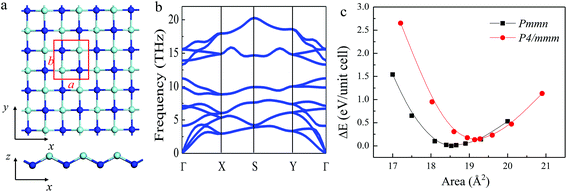
The optimized atomic structure of a stable 2D t-YN monolayer is displayed in Fig. 1. The t-YN unit cell containing two yttrium and two nitrogen atoms crystallizes in the orthorhombic lattice with a space group Pmmn, exhibiting D2h symmetry. Each atom in the unit cell is bonded to four neighboring atoms. Fig. 1c shows energy vs. area curve for the t-YN monolayer. The optimized lattice constants are: a = 4.024 Å and b = 4.605 Å, respectively. Along the x direction, the t-YN monolayer is buckled into a zigzag line, while along the y direction, it exhibits a bilayer structure. The bond angle along the x direction is 125.9°, and the buckling is 1.325 Å. The bond length of Y–N is 2.259 Å along the x direction, but 2.322 Å along the y direction. The lattice parameters are in good agreement with the result reported by Liu.32 Due to the buckling structure, the 2D t-YN monolayer shows anisotropic mechanical behavior: Young's modulus is up to 83.4 N m−1 along the y direction, but much softer along the x direction, reduced to 43.6 N m−1, which is attributed to the zigzag buckling feature.To investigate the thermodynamic stability of the ground-state structure of the 2D t-YN monolayer, we also calculated the cohesive energy. It is expressed as follows:
| ΔEYN = (2EY + EN − EYN)/4 | (1) |
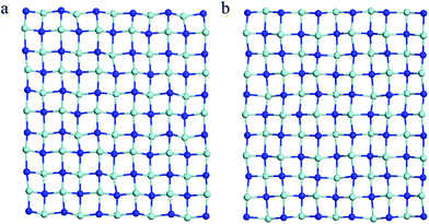 | ||
| Fig. 2 The snapshot of the equilibrium structure of the t-YN monolayer at (a) 800 K and (b) 1300 K at the end of 5 ps first-principles molecular dynamics (MD) simulation. | ||
3.2 Electronic structure of the 2D t-YN monolayer
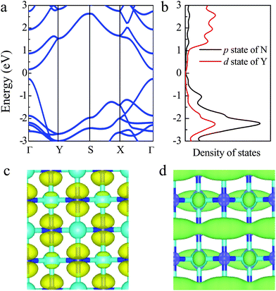
Based on the stability of the 2D t-YN monolayer, the electronic properties were investigated. To avoid the underestimated band gap in semiconductors by the PBE functional, the results calculated by using the HSE06 functional are adopted. The band structure of the 2D t-YN monolayer is clearly displayed in Fig. 3a. Different from the indirect band gap in the tetragonal TiC monolayer,23 the 2D t-YN monolayer is a direct band gap semiconductor with a band gap of 0.55 eV at the Γ point, which is in agreement with the previous result.32 To gain further insight into the electronic properties of the 2D t-YN monolayer, the partial densities of electronic states were calculated (Fig. 3b). The valence band maximum (VBM) is mainly contributed by the p-orbital of N atoms, while the conduction band minimum (CBM) is composed of the d-orbital of Y atoms and the p-orbital of N atoms. Electronic orbital analysis confirms that the CBM at the Γ point is from the hybridization of N 2px and Y 4dz2 states, while the VBM at the Γ point is from the N 2py states, as illustrated by the charge density distributions in Fig. 3c and d.Furthermore, we found that the charge density distributions of CBM and VBM are highly direction-dependent, which indicates that the electronic properties of the 2D t-YN monolayer are direction-dependent: anisotropic. It can also be concluded by the band structure of 2D t-YN (Fig. 3a) that the top of the valence band along the Γ–Y direction has much more significant dispersion than that along the Γ–X direction. But the situation for the bottom of the conduction band is opposite: the band along the Γ–X direction has more significant dispersion. The anisotropic band dispersions in the 2D t-YN monolayer imply the anisotropic electronic properties. To obtain deeper insight into the anisotropic electronic properties of the 2D t-YN monolayer: we analyzed the effective masses of electrons and holes in Fig. 4a and b. The effective mass is proportional to the inverse of the curvature of the band dispersion. The greater band dispersion means the lower effective mass. So, both the effective masses of the electrons and holes are highly anisotropic. The direction-dependent effective masses of the electrons are illustrated in Fig. 4a, which shows an approximate “8” shape. The effective mass is 0.313me along the x direction, and 0.920me along the y direction. For the holes, the in-plane anisotropy is rotated by 90°, while retaining the approximate “8” shape (i.e., “∞” shape) (Fig. 4b). The effective mass is 0.413me along the x direction, and 0.197me along the y direction. The low effective masses of the electrons and holes are comparable to those in other 2D materials, such as phosphorene,12,14 TiS3,47 and MoS2.48 The in-plane anisotropic ratios of the effective masses of electrons and holes in the 2D t-YN monolayer are 2.94 and 2.10, respectively, which are smaller than that in phosphorene (about 6.59).12 The electric conductance in the 2D t-YN monolayer is also anisotropic due to the anisotropic effective masses of the carrier.
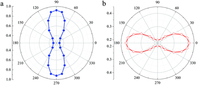 | ||
| Fig. 4 The direction-dependent effective masses of (a) the electrons and (b) holes of the t-YN monolayer. | ||
Our calculations indicate that the 2D t-YN monolayer shows strong anisotropy in mechanical and electronic properties due to the anisotropic structure. The t-YN monolayer possesses the same structure as the 2D tetragonal TiN, which was predicted to be ferroelastic.25 It is interesting if the 2D t-YN monolayer is ferroelastic, because it means that the properties, including the anisotropy, can be switched upon applying external stress. After a systematic study, we concluded that the 2D t-YN monolayer is a ferroelastic material.
3.2 Ferroelasticity of the 2D t-YN monolayer
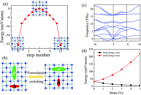
The ferroelasticity of the 2D t-YN monolayer was studied by using the CI-NEB method to compute the transition path and the activation energy barrier. The initial state and the final state are the same state (Pmmn) with structures rotated by 90° as shown in the inset of Fig. 5a. The intermediate state between the initial state and the final state is in a square lattice with the space group of P4/mmn, also displayed in the inset of Fig. 5a. The energy vs. area curve for the square YN monolayer is shown in Fig. 1c. The lattice parameters of the intermediate state are optimized as a = b = 4.375 Å. We also studied the phonon dispersion of the square YN monolayer, as shown in Fig. 5c. Clearly, the calculated phonon dispersion of the intermediate state exhibits imaginary frequencies around the Γ point, indicating the instability of the intermediate state. It is consistent with the theory of ferroelastic phase transition. The energy profile has been plotted as a function of step number (step 6) within the NEB method, as shown in Fig. 5a. The reaction paths from the initial state to the intermediate state and from the intermediate state to the final state were proved to be identical, which is grounded in symmetry. The activation energy barrier for the ferroelastic transition between the initial state and the final state for the 2D t-YN monolayer is computed to be 33 meV per atom with a reversible ferroelastic strain of 14.4% (the reversible ferroelastic strain is defined as (b/a − 1) × 100%). Furthermore, the activation energy barrier enlarges to 220 meV per atom as strain increases to 5% along the b direction, while it decreases to 6 meV per atom as strain increases to 5% along the a direction. When the strain is applied along one direction, the lattice parameter of the other direction is fully relaxed.As we know, the anisotropies are strongly related to their anisotropic structures. As the 2D t-YN monolayer is ferroelastic, the anisotropic structure can be rotated by 90° under external stress, leading to the anisotropic properties associated with the x and y directions being switched. For example, as illustrated in Fig. 5b, under the ferroelastic transition, the anisotropies in the effective masses of the electrons and holes for the 2D t-YN monolayer will be rotated by 90°. As a result, the electric conductance in the 2D t-YN monolayer can be switched between the x and y directions by applying external stress, so do the anisotropic mechanical properties.
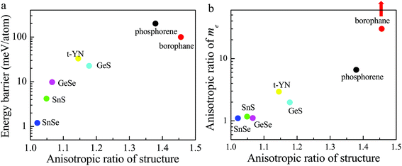
However, up to now, the 2D ferroelastic t-YN monolayer has not shown any other advantages compared to other 2D ferroelastic materials, such as phosphorene,28 borophane,30 and monochalcogenides.29 We summarized the energy barriers vs. the anisotropic ratios of the reported 2D ferroelastic materials in Fig. 6a. The anisotropic ratio of the structure is defined as b/a. The difference between the reversible ferroelastic strain and the anisotropic ratio is 1. As shown in Fig. 6a, the larger the anisotropic ratio of the structure, the higher the energy barrier in general. The energy barrier for the 2D t-YN monolayer is lower than those for phosphorene (200 meV per atom)29 and borophane (100 meV per atom),30 but significantly higher than those for monochalcogenides (1.2, 4.2, 9.8, and 22.6 meV per atom for SnSe, SnS, GeSe, and GeS, respectively).29 The energy barrier is not the higher the better. Because a high energy barrier means that it is difficult to realize the ferroelastic switching in experiments. For example, the energy barrier for phosphorene is about 200 meV, and the reversible ferroelastic strain is about 37.9%, almost the highest value known to date in ferroelastic materials. It means that it should overcome a strain of 37.9%, if the ferroelastic transition happens in phosphorene.
But the energy barrier is also not the lower the better, because a low energy barrier indicates the weakly anisotropic ratio of the structure, which is highly related to the anisotropic properties. So the low energy barrier suggests that the anisotropies are weak. We take the anisotropic effective mass of the electron for example. Fig. 6b shows the anisotropic ratio of the electron effective mass vs. the anisotropic ratio of the structure for the reported 2D ferroelastic materials. The anisotropic ratio of the electron effective mass is defined as my/mx or mx/my to make sure it is >1. As shown in Fig. 6b, there is almost no anisotropy in the electron effective mass for SnSe (1.07), SnS (1.17), and GeSe (1.11),49 because the energy barriers for SnSe, SnS, and GeSe are very low, less than 10 meV per atom. For GeS and t-YN, the energy barriers are moderate, 22.6 and 33 meV per atom, respectively. The anisotropic ratio of the electron effective mass is significantly enhanced, 1.95 and 2.94, respectively. Furthermore, phosphorene and borophane have very large energy barriers. The anisotropic ratio of the electron effective mass in phosphorene is also very high (6.59). For borophane, it is infinite,30 because it is a semimetal with a Dirac point across the Fermi level in one direction, but a semiconductor in the other direction. So, the moderate energy barrier endows the 2D t-YN monolayer with great advantages in controlling the anisotropies experimentally.
4. Conclusion
In summary, using first-principles calculations, we have predicted the strong anisotropic mechanical and electronic properties of a 2D t-YN monolayer. We find that the 2D t-YN monolayer is a ferroelastic semiconductor with a low direct band gap of 0.55 eV. The anisotropic ratio of the effective mass along the two directions is 2.94 and 2.10 for the electron and hole, respectively. The ferroelasticity suggests that the in-plane anisotropies of the 2D t-YN monolayer can be further switched by applying external stress. The moderate energy barrier for ferroelastic switching makes the 2D t-YN monolayer a very promising candidate to control the anisotropies by strain in experiments. We hope our theoretical studies will promote the experimental realization of the anisotropic 2D t-YN monolayer and attract much attention in the applications of designing novel 2D ferroelastic materials.Conflicts of interest
There are no conflicts to declare.Acknowledgements
This work was supported by the Fundamental Research Funds for the Central Universities, a project funded by the Priority Academic Program Development of Jiangsu Higher Education Institutions (PAPD). We are grateful for the support of NSFC (No. 11134004, 51672126 and 51372111). The calculations were performed on parallel computers at the High Performance Computing Center (HPCC) of Nanjing University.References
- K. S. Novoselov, A. K. Geim, S. Morozov, D. Jiang, Y. Zhang, S. A. Dubonos, I. Grigorieva and A. Firsov, Science, 2004, 306, 666–669 CrossRef CAS PubMed.
- B. Radisavljevic, A. Radenovic, J. Brivio, V. Giacometti and A. Kis, Nat. Nanotechnol., 2011, 6, 147–150 CrossRef CAS PubMed.
- W. S. Yun, S. W. Han, S. C. Hong, I. G. Kim and J. D. Lee, Phys. Rev. B: Condens. Matter Mater. Phys., 2012, 85, 033305 CrossRef.
- K. F. Mak, C. G. Lee, J. Hone, J. Shan and T. F. Heinz, Phys. Rev. Lett., 2010, 105, 136805 CrossRef PubMed.
- A. J. Du, S. Sanvito, Z. Li, D. W. Wang, Y. Jiao, T. Liao, Q. Sun, Y. H. Ng, Z. H. Zhu, R. Amal and S. C. Smith, J. Am. Chem. Soc., 2012, 134, 4393–4397 CrossRef CAS PubMed.
- C. Jin, F. Lin, K. Suenaga and S. Iijima, Phys. Rev. Lett., 2009, 102, 195505 CrossRef PubMed.
- F. Schedin, A. K. Geim, S. V. Morozov, E. W. Hill, P. Blake, M. I. Katsnelson and K. S. Novoselov, Nat. Mater., 2007, 6, 652–655 CrossRef CAS PubMed.
- S. H. Zhang, J. Zhou, Q. Wang, X. S. Chen, Y. Kawazoe and P. Jena, Proc. Natl. Acad. Sci. U. S. A., 2015, 112, 2372–2377 CrossRef CAS PubMed.
- X. Qian, J. Liu, L. Fu and J. Li, Science, 2014, 346, 1344–1347 CrossRef CAS PubMed.
- H. M. Liu, B. Xu, J.-M. Liu, J. Yin, F. Miao, C.-G. Duan and X. G. Wan, Phys. Chem. Chem. Phys., 2016, 18, 14222–14227 RSC.
- H. Liu, A. T. Neal, Z. Zhu, Z. Luo, X. F. Xu, D. Tománek and P. D. Ye, ACS Nano, 2014, 8, 4033–4041 CrossRef CAS PubMed.
- J. Qiao, X. Kong, Z.-X. Hu, F. Yang and W. Ji, Nat. Commun., 2014, 5, 4475 CAS.
- V. Tran, R. Soklaski, Y. F. Liang and L. Yang, Phys. Rev. B: Condens. Matter Mater. Phys., 2014, 89, 235319 CrossRef.
- R. X. Fei and L. Yang, Nano Lett., 2014, 14, 2884–2889 CrossRef CAS PubMed.
- L. C. Gomes, P. E. Trevisanutto, A. Carvalho, A. S. Rodin and A. H. Castro Neto, Phys. Rev. B: Condens. Matter Mater. Phys., 2016, 94, 155428 CrossRef.
- H. D. Wang, X. X. Li, P. Li and J. L. Yan, Nanoscale, 2017, 9, 850–855 RSC.
- G. Z. Qin, Z. Z. Qin, W. Z. Fang, L. C. Zhang, S. Y. Yue, Q. B. Yan, M. Hu and G. Su, Nanoscale, 2016, 8, 11306–11319 RSC.
- G. S. Shi and E. Kioupakis, Nano Lett., 2015, 15, 6926–6931 CrossRef PubMed.
- E. F. Liu, Y. J. Fu, Y. J. Wang, Y. Q. Feng, H. M. Liu, X. G. Wan, W. Zhou, B. G. Wang, L. B. Shao and C. H. Ho, Nat. Commun., 2015, 6, 6991 CrossRef CAS PubMed.
- X. B. Li, S. Y. Xie, H. Zheng, W. Q. Tian and H. B. Sun, Nanoscale, 2015, 7, 18863 RSC.
- A. J. Mannix, X.-F. Zhou, B. Kiraly, J. D. Wood, D. Alducin, B. D. Myers, X. Liu, B. L. Fisher, U. Santiago, J. R. Guest, M. J. Yacaman, A. Ponce, A. R. Oganov, M. C. Hersam and N. P. Guisinger, Science, 2015, 350, 1513 CrossRef CAS PubMed.
- X.-F. Zhou, X. Dong, A. R. Oganov, Q. Zhu, Y. Tian and H.-T. Wang, Phys. Rev. Lett., 2014, 112, 085502 CrossRef.
- Z. H. Zhang, X. F. Liu, B. I. Yakobson and W. L. Guo, J. Am. Chem. Soc., 2012, 134, 19326–19329 CrossRef CAS PubMed.
- X. Zhang, Z. H. Zhang, X. D. Zhao, D. H. Wu, X. Zhang and Z. Zhou, J. Mater. Chem. A, 2017, 5, 2870–2875 CAS.
- L. J. Zhou, Z. W. Zhuo, L. Z. Kou, A. J. Du and S. Tretiak, Nano Lett., 2017, 17, 4466–4472 CrossRef CAS PubMed.
- S. Anand, K. Thekkepat and U. V. Waghmare, Nano Lett., 2016, 16, 126–131 CrossRef CAS PubMed.
- A. V. Kuklin, A. A. Kuzubov, E. A. Kovaleva, N. S. Mikhaleva, F. N. Tomilin, H. Lee and P. V. Avramov, Nanoscale, 2017, 9, 621–630 RSC.
- M. Wu and X. C. Zeng, Nano Lett., 2016, 16, 3236–3241 CrossRef CAS PubMed.
- H. Wang and X. Qian, 2D Mater., 2017, 4, 015042 CrossRef.
- L. Z. Kou, Y. D. Ma, C. Tang, Z. Q. Sun, A. J. Du and C. F. Chen, Nano Lett., 2016, 16, 7910–7914 CrossRef CAS PubMed.
- L. Mancera, J. A. Rodríguez and N. Takeuchi, J. Phys.: Condens. Matter, 2003, 15, 2625–2633 CrossRef CAS.
- J. Liu, X. B. Li, H. Zhang, W. J. Yin, H. B. Zhang, P. Peng and L. M. Liu, J. Appl. Phys., 2014, 115, 093504 CrossRef.
- J. Li, G. Y. Gao, Y. Min and K. L. Yao, Phys. Chem. Chem. Phys., 2016, 18, 28018–28023 RSC.
- Z. F. Liu, J. Y. Liu and J. J. Zhao, Nano Res., 2017, 10, 1972–1979 CrossRef CAS.
- S. Gong, C. Z. Zhang, S. Wang and Q. Wang, J. Phys. Chem. C, 2017, 121, 10258–10264 CAS.
- G. Kresse and J. Furthmüller, Phys. Rev. B: Condens. Matter Mater. Phys., 1996, 54, 11169 CrossRef CAS.
- G. Kresse and J. Furthmüller, Comput. Mater. Sci., 1996, 6, 15 CrossRef CAS.
- J. P. Perdew, K. Burke and M. Ernzerhof, Phys. Rev. Lett., 1996, 77, 3865 CrossRef CAS PubMed.
- D. C. Langreth and M. Mehl, Phys. Rev. B: Condens. Matter Mater. Phys., 1983, 28, 1809 CrossRef CAS.
- A. D. Becke, Phys. Rev. A, 1998, 38, 3098 CrossRef.
- J. Heyd, G. E. Scuseria and M. Ernzerhof, J. Chem. Phys., 2003, 118, 8207 CrossRef CAS.
- A. Togo, F. Oba and I. Tanaka, Phys. Rev. B: Condens. Matter Mater. Phys., 2008, 78, 134106 CrossRef.
- G. J. Martyna, M. L. Klein and M. Tuckerman, J. Chem. Phys., 1992, 97, 2635 CrossRef.
- G. Henkelman and H. Jónsson, J. Chem. Phys., 2000, 113, 9978–9985 CrossRef CAS.
- S. Reich, C. Thomsen and P. Ordejón, Phys. Rev. B: Condens. Matter Mater. Phys., 2002, 65, 153407 CrossRef.
- S. Cahangirov, M. Topsakal, E. Aktürk, H. Şahin and S. Ciraci, Phys. Rev. Lett., 2009, 102, 236804 CrossRef CAS PubMed.
- J. Dai and X. C. Zeng, Angew. Chem., Int. Ed., 2015, 54, 7572–7576 CrossRef CAS PubMed.
- H. Shi, H. Pan, Y. W. Zhang and B. I. Yakobson, Phys. Rev. B: Condens. Matter Mater. Phys., 2013, 87, 155304 CrossRef.
- A. Shafique and Y. H. Shin, Sci. Rep., 2017, 7, 506 CrossRef PubMed.
- C. Ataca, H. Şahin and S. Ciraci, J. Phys. Chem. C, 2012, 116, 8983–8999 CAS.
| This journal is © The Royal Society of Chemistry 2018 |

