 Open Access Article
Curvature-dependent flexible light emission from layered gallium selenide crystals†
Ching-An Chuanga,
Min-Han Lina,
Bo-Xian Yeha and
Ching-Hwa Ho *ab
*ab
aGraduate Institute of Applied Science and Technology, National Taiwan University of Science and Technology, Taipei 106, Taiwan. E-mail: chho@mail.ntust.edu.tw; Fax: +886 2 27303733; Tel: +886 2 27303772
bGraduate Institute of Electro-Optical Engineering, Department of Electronic and Computer Engineering, National Taiwan University of Science and Technology, Taipei 106, Taiwan
First published on 12th January 2018
Abstract
Flexible optoelectronics devices play an important role for technological applications of 2D materials because of their bendable, flexible and extended two-dimensional surfaces. In this work, light emission properties of layered gallium selenide (GaSe) crystals with different curvatures have been investigated using bending photoluminescence (BPL) experiments in the curvature range between R−1 = 0.00 m−1 (flat condition) and R−1 = 30.28 m−1. A bendable and rotated sample holder was designed to control the curvature (strain) of the layered sample under upward bending uniformly. The curvature-dependent BPL results clearly show that both bandgaps and BPL intensities of the GaSe are curvature dependent with respect to the bending-radius change. The main emission peak (bandgap) is 2.005 eV for flat GaSe, and is 1.986 eV for the bending GaSe with a curvature of 30.28 m−1 (the maximum bending conditions in this experiment). An obvious redshift (i.e. energy reduction) for the GaSe BPL peak was detected owing to the c-plane lattice expansion by upward bending. The intensities of the corresponding BPL peaks also show an increase with increasing curvature. The correlations between BPL peak intensity, shiny area and bond-angle widening of the bent GaSe under laser excitation have been discussed. The lattice constant versus emission energies of the bending GaSe was also analyzed. An estimated lattice constant vs. bandgap relation was present for further application of the layered GaSe in bendable flexible light-emission devices.
1. Introduction
Since the isolation of graphene in 2004,1 graphene still remains one of the hottest research topics in materials science. Nowadays the focus has shifted from purely researching graphene itself to other 2D semiconductors, and then to their applications, especially for making use of their “natural flexibility”. Similar to graphene, 2D chalcogenide semiconductors such as III–VI layered-type chalcogenides, with the properties of being bendable, curved, and ultra-thin, are considered as rising-star materials for next-generation, bendable optoelectronics and electronics. Gallium selenide (GaSe) is one of the 2D III–VI layered-type chalcogenides with a hexagonal layer structure and its bandgap is around 2 eV at room temperature.2,3 Because the interlayers of GaSe crystal are connected via van der Waals bonds, it can be exfoliated to few layer or even monolayers for further device application.4 It means that GaSe could be considered as a flexible material even while it is exfoliated from thick to thin multilayers. For light-emitting capability, unlike MoSe2 which has only enhanced photoluminescence (PL) efficiency as a monolayer, the PL intensity of monolayer GaSe vanishes, and increases with the layer thickness increasing to multilayer or bulk form.5 Multilayer and bulk GaSe tend to be a direct band-edge like material while multilayer MoSe2 is an indirect semiconductor. Many of previous reports had claimed that the GaSe is indirect6–8 with an indirect band edge lower than that of the direct one by 53 meV.8 However, for the c-plane optical property, the indirect transition of geometric effect on the layered GaSe is very weak because the absence of spin–orbit coupling and it would be forbidden.8 The c-plane multilayer GaSe thus could own high-luminescence efficiency and high photocurrent owing to its direct-band-edge like optical transition. From this direct-band-edge like c plane, the layered GaSe eventually becomes the most excellence and utmost representative role in the GaSe1−xSx (0 ≤ x ≤ 1) series layers.9 The GaSe can be used for nonlinear optical applications in the 8–15 μm wavelength region.3 A micro-cavity GaSe with strong red-light lasing has also been fabricated and announced to be a practical 2D-material laser.10 With the 2D flexible capability, more potential applications such as flexible display and bendable photodetector for the GaSe multilayer could be further expected.The bandgap is the most important parameter of a material. For a semiconductor, its bandgap determines optical property, electrical and optoelectronic behaviours. The bandgap of a conventional semiconductor is not adjustable owing to its rigidity with fixed crystal structure. However, when bending the 2D GaSe, its bandgap (i.e. the c-plane direct gap) is tunable. It can provide great flexibility when designing electronic devices. So far, many researchers are still keen to explore mechanisms and develop methods for tuning bandgap in semiconductors. The methods include changing ambient temperature,11 strain engineering,12 changing thickness of compound semiconductor from bulk crystal to thin layer,13,14 exerting an external electric field,15 chemical doping,16–18 or by synthesizing the 2D semiconductors with different bandgaps.4,13 Among those methods, strain engineering is more attractive and applicable when a flexible optoelectronics device is under normally-operated condition. Our previous research has found that the mechanical bending would also enhance the light intensity of photoluminescence peak of 2D InSe layered semiconductor.19 Further investigations for the correlated phenomena are still very limited. Recently, the photoluminescence enhancement and bandgap change for GaSe nanosheets on polyethylene terephthalate (PET) substrate were observed by bending PET with deformed strain.20 The result showed the bandgap is decreased with tensile strain existed in the GaSe layer. However, the softy and easy-deformation character of the PET resulted in layer wrinkles and non-uniform strain distribution on the GaSe nanosheets, which caused the difficulty on estimate of actual strain effect.
In this study, high-quality GaSe layered crystals have been grown by vertical Bridgman (VB) method. A rotatable and bendable sample holder together with one stainless steel sheet (SSS, t ∼ 100 μm) was designed to implement curvature-dependent BPL measurements. A RAMaker micro-PL and micro-Raman system equipped with one 532 nm laser was used to facilitate the BPL experiment. A 3 μm thick GaSe layer crystal was closely attached on smooth SSS surface by crazy glue in order to get high PL intensity and uniformity of strain distribution in whole layer. The measurements were done with different curvatures from flat condition (curvature R−1 = 0 m−1), step by step, increased to R−1 = 30.28 m−1. When the curvature is increased, the BPL intensity of GaSe is also increased while the bandgap is gradually decreased. The mechanisms of PL enhancement and bandgap reduction of the GaSe under upward bending have been detailed analyzed and discussed. The PL enhancement is due to the increase of shiny area and the widening of acceptance solid angle when the laser shined on sample under upward bending. A relationship of lattice constant versus energy-gap change in the strained GaSe, i.e. a = 5.3167 − 1.3357Eg + 0.2757Eg2 (Å), has also been obtained for future application of the layered gallium selenide in flexible or bendable optoelectronics devices.
2. Experimental section
Crystal growth
Single crystals of GaSe layer compound were grown by vertical Bridgman method.21,22 Appropriate amount of gallium and selenium with 99.999% purity were put into a carbon-coated ampoule of 1.0 cm inner diameter (ID), which was then evacuated and sealed in vacuum with about 10−6 Torr. The ampoule was heated to the melting point of synthesized material in a rocking furnace and hold at this temperature for one day. The lowering rate of the ampoule in the VB furnace is set as ∼1.5 mm per hour and the temperature gradient was greater than 45 °C cm−1. The ampoule was rotated at a constant speed of 15 cycles per minute. At the end of the process the ampoule was quenched to room temperature. The obtained crystals were essentially layer type and dark-red colored with an area size up to ∼tens mm2 and thickness ∼ hundreds μm. X-ray diffraction (XRD) measurements (see ESI – Fig. S1†) revealed two-layer hexagonal (2H) phase for the as-grown GaSe crystals with the calculated lattice constants a = 3.75 Å and c = 15.94 Å. Electron probe microanalysis verified the stoichiometric content approximately Ga:Se ≈ 1:1 with a slight chalcogen deficiency.Optical measurement
The BPL measurements of the GaSe layered crystal were implemented via a RAMaker micro-PL & micro-Raman integrated system with a 532 nm solid state laser as the excitation source. An Olympus objective lens (50×, working distance 8 mm) acted as the inter-connection medium between incident laser, layered sample, and all the reflected and scattered lights. The power density of the excited laser was set as 0.3 W cm−2, and laser spot area onto flat sample was measured to be ∼3.1416 mm2. The micro-PL measurement was done at room temperature.Measurement of curvature for bending GaSe
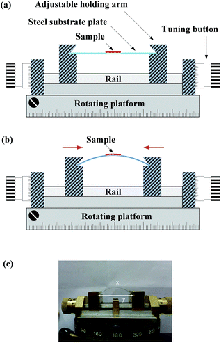
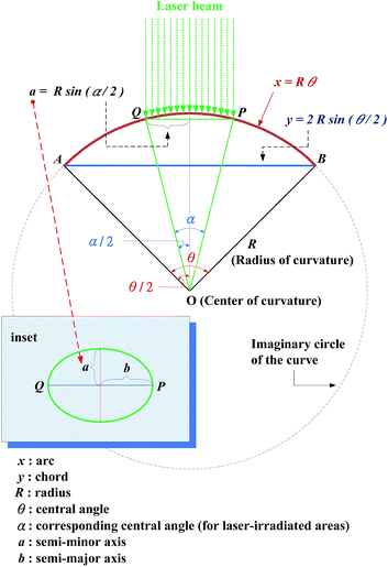
For curvature-dependent BPL measurements, the test sample is a layered GaSe with thickness of 30 μm and area of 8 mm2. The layered GaSe, grown by a conventional VB technique, was firmly attached onto the middle section of a bendable stainless steel with dimension of 40 mm (length) × 20 mm (width) × 0.103 mm (thick) using crazy glue (i.e. 3M Scotch instant glue, gel type). When the steel was bended, the layered GaSe sample was also bended accordingly. In order to bend the layered GaSe uniformly, a rotatable holder with adjustable bending mechanism was designed and the SSS plate was then placed on the holder with two arms on both sides as shown in Fig. 1(a). Initially the distance between the two arms of the holder was set to be exactly the length of the SSS (40 mm) with flat condition. Decreasing the distance between two arms by exerting horizontal stress from the two arms, the SSS plate will then alter its shape from a flat surface to an upward curved surface as indicated in Fig. 1(b). The operation of the mechanical design is shown in the picture of Fig. 1(c). As shown by a dashed-line circle in Fig. 2, the bending steel, with a length of 40 mm, could be approximately considered as a part curve of representative circle with a radius R. The arc, marked x, is exactly the bending SSS plate with a constant length of 40 mm expressed as| x = Rθ, | (1) |
 | (2) |
The ratio of x to y is a function of θ expressed as:
 | (3) |
Once the ratio of x to y is measured using the ruler in the holder in Fig. 1(b), the central angle θ can be calculated by eqn (3), and then the corresponding radius R is obtained using eqn (1). In order to avoid measurement distortion, the curvature radius (bending condition) of the BPL measurement was limited and not over-bending with the minimum curvature radius R = 33.03 mm in the BPL experiment. This bending limit is like a maximum view angle of a flexible display suitable for normally upward operation.
Calculation of laser illuminated area on the bended GaSe surface
In BPL measurement, when the laser beam hit the flat test sample, the laser-irradiated area is a circle with a radius of 1.0 mm as measured. As the SSS plate is bended, the laser-irradiated area increases accordingly due to geometrical changes from 2D plane to 3D cylinder surface. It means that the projected area becomes an ellipse instead of a circle when the curved surface flattened. For measuring the laser-irradiated ellipse area under different bending conditions, the semi-minor axis “a” and semi-major axis “b” of the ellipse must be determined as indicated in the inset of Fig. 2. Arc QP illustrated in Fig. 2 represents the extending axis of the cross-section of the laser-irradiated surface, and its length equals to 2b. The arc length can also be expressed as the product of the radius R and the central angle α:| QP = Rα = 2b. | (4) |
The length of the chord QP equals to 2a (a is semi-minor axis of ellipse and always remains the same no matter how the steel plate is bended) and a can be obtained from:
 | (5) |
The ratio of laser arc (arc QP on sample) to the steel arc (arc AB) in Fig. 2 is:
 | (6) |
Because the measured value of a is 1.0 mm, and R can be obtained from eqn (1) to eqn (3), the angle α can be hence obtained from eqn (5). The semi-major axis is then b = Rα/2 and the area of laser-illuminated ellipse is therefore equal to A = πab.
3. Results and discussion
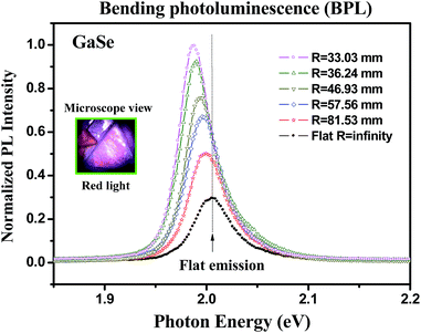
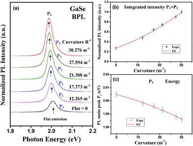
Fig. 3 shows the curvature-dependent BPL spectra of the c-plane GaSe with different upward bending radius (referred to Fig. 2) from R = ∞ (flat) to R = 33.03 mm at room temperature. The PL intensity is enhanced with the curve bending increased while the bandgap of the layer is gradually decreased. At flat condition, the main bandgap (peak) is at 2.005 eV with a normalized PL intensity I ≈ 0.274 (i.e. set the maximum PL intensity as I = 1.0 at R = 33.03 mm), whereas the peak shifts to ∼1.986 eV under the maximum bending condition of R = 33.03 mm. The inset of Fig. 3 clearly shows a red-color emission from the microscope image of the GaSe multilayer in micro-PL system. As shown in Fig. 3, the PL spectra of GaSe under flat and bending conditions show approximately two peaks that consisted in the PL peak feature. The detailed analysis and line-shape fitting of the BPL spectra using double peak features are shown in Fig. 4(a). The dashed lines are the experimental BPL data and solid curves are those of Lorentzian line-shape fits. For the flat condition (R−1 = 0), the PL spectrum has one peak feature at P1 ≈ 2.005 eV and the other peak at P2 ≈ 2.047 eV, which they can approximately achieve the fitting. With the bending curvature is increased, two peaks are shift to P1 ≈ 1.998 eV and P2 ≈ 2.041 eV at the curvature of R−1 = 12.265 m−1. The occurrence of two peaks in the GaSe multilayer is attributed to the as-grown layered crystal might exist two stacking phases of two-layer hexagonal (2H) ε and 2H β stacking23 such as the indication of high-resolution transmission-electron microscopy (HRTEM) image as displayed in Fig. S2(a) in ESI.† The main difference between the two stacking phases of 2H-ε GaSe and 2H-β GaSe depends on the Se–Ga–Ga–Se fundamental units are stacking along c axis [see the insets of Fig. S2(a)†]. In the case of β-GaSe, the fundamental Se–Ga–Ga–Se units are stacking with the Se atoms of the top layer placed above the Ga atoms of the bottom layer while the Ga atoms of the top layer located above the Se atoms of the bottom layer. The Se–Ga–Ga–Se units in the ε-GaSe stacking are shifted and misalignment as depicted in Fig. S2(a).† The β and ε modifications have different bandgaps and their energy separation is around 0.04–0.05 eV in GaSe.24 The selection-area electron diffraction (SEAD) pattern and fast Fourier transform (FFT) result in Fig. S2(b) and (c)† also showed clearly dotted pattern. All the HRTEM results verified high crystalline quality of the as-grown GaSe multilayer and the crystal possesses mixed phases of 2H β and ε stacking. Therefore, it is inferred that the lower-energy P1 peak in Fig. 4(a) might come from the 2H ε-GaSe phase while the higher-energy P2 peak is correlated with the bandgap of the β-GaSe stacking. When the laser impinged on the layer and excited the band edge of GaSe, the excited hot carriers will relax their energy and result in more intense P1 peak (by ε-GaSe) with lower energy states' recombination. However, the higher-energy P2 peak (by β-GaSe) will also be enhanced when the GaSe layer is under bending conditions as observed in Fig. 4(a). The P1 and P2 peaks simultaneously show energy redshift with the bending curvatures of GaSe are increased from R−1 = 0 to R−1 = 30.276 m−1. The intensities of the P1 and P2 peaks are also enhanced with increasing curvatures of GaSe from R−1 = 0 to R−1 = 30.276 m−1 as shown in Fig. 4(a). It is noticed that the full-width half maximum (FWHM) of the PL peak features of P1 and P2 are also broadened with the curvature increases due to the lattice constant changed under strain. The strain-induced effect may broaden the line width of the PL feature under the bent state. Besides, we have also observed the recovered PL emission of the layered GaSe back to the flat condition. The PL emission features are similar before and after the SSS bending. The PL emission feature at ∼2 eV may infer to come from the direct band edge of the c-plane GaSe, which is different from those of the other defect emissions with energies lower than 1.8 eV coming from the imperfection states of the GaSe samples.6In order to analyze curvature-dependent PL intensity change of the GaSe layer, the PL peaks of P1 and P2 in Fig. 4(a) are combined for analysis. Fig. 4(b) shows the variations of integrated intensity of P1 + P2 as a function of bending curvatures. The solid squares are the experimental data obtained by the line-shape fits in Fig. 4(a), and the solid line is the least-square fit of the normalized PL intensities versus curvature using a relation of I(x) = a0 + a1x + a2x2. The obtained fitting parameters are a0 = 0.288 ± 0.012, a1 = 0.017 ± 0.003 m, and a2 = (2.95 ± 1.05) × 10−4 m2. It is obvious that the best fit of the normalized intensity vs. curvature (red line) in Fig. 4(b) must contain both linear-term parameter a1 and square-term parameter a2. The result implies that the PL enhancement of the layered GaSe under upward bending should include two mechanisms of laser illuminated area and emission solid angle. The origin of BPL enhancement in GaSe will be discussed later in Fig. 6.
Fig. 4(c) shows the curvature-dependent peak position of P1 of layered GaSe with representative error bars that obtained from the Lorentzian line-shape fits of the BPL spectra. Because the P1 is more prominent when a GaSe flexible device is operated with upward bending [see Fig. 4(a)], the lower-energy peak P1 (with respect to P2) is hence delegate for the analysis of curvature-dependent energy shift in the GaSe luminescences. As the curvature is increased from R−1 = 0, 12.265, 17.373, 21.308, 27.594, to R−1 = 37.276 m−1, the bandgap gradually decreases from P1 ≈ 2.005, 1.998, 1.996, 1.993, 1.988, to P1 ≈ 1.986 eV such as those shown in Fig. 4(c). The energy reduction should be come from the tensile strain existed in the outer-layer plane of the GaSe under upward bending, resulting in lattice expansion. The red solid line in Fig. 4(c) is the least-square fit of P1 bandgap energy vs. curvature using the relation containing linear term b1 and square term b2 as E(x) = b0 + b1x + b2x2 eV. The obtained values of fitting parameters are b0 = 2.005 ± 0.002 eV, b1 = −(4.3 ± 1.3) × 10−4 eV m, and b2 = −(6 ± 3) × 10−6 eV m2, respectively. This relationship can be used to future estimate curvature-dependent bandgap shift of GaSe under normally bending operation.
To further study the dependence of lattice constant vs. energy gap of the layered GaSe, transmittance absorption result and in-plane lattice constant a of the ternary layered compounds GaSe0.9S0.1, GaSe0.8S0.2, GaSe0.7S0.3, and GaSe0.6S0.4 of similar crystal structure18,19 have also been included for comparison and analysis. Those experimental results were done by our laboratory previously.18,19 The values of lattice constant and bandgap have been determined to be a = 3.747 Å and Eg = 2.005 eV for flat GaSe, a = 3.736 Å and Eg = 2.051 eV for GaSe0.9S0.1, a = 3.724 Å and Eg = 2.121 eV for GaSe0.8S0.2, a = 3.714 Å and Eg = 2.195 eV for GaSe0.7S0.3, and a = 3.704 Å and Eg = 2.276 eV for GaSe0.6S0.4, respectively. The data are shown by solid squares (with representative errors) in Fig. 5.
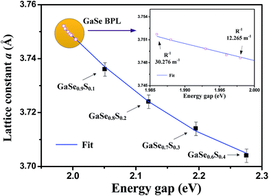 | ||
| Fig. 5 The analysis of in-plane lattice constant a versus bandgaps in layered GaSe1−xSx (0 ≤ x ≤ 0.4) series compounds with similar structure18,19 together with those of the curvature-dependent bending GaSe results are also included for comparison. The fitting result [a(Eg), depicted as the blue solid line] shows a good fit that extending to the BPL region of different curvatures of GaSe as shown in the inset. It can be utilized to analyze lattice constant vs. bandgap change in bending GaSe. | ||
It should be mentioned that energy bandgap variations in the GaSe1−xSx (0 ≤ x ≤ 0.4) crystal series are maybe mainly caused by two mechanisms: one is the lattice constant change, and the other is the chemical constituent change when the Se substitutes with S. The band-structure change of electronic states of the GaSe1−xSx with S substitution into the Se site in the GaX (X = S, Se) need be detailed refined by further theoretical calculations. However, in this study, we have not considered this part and have only focused on the lattice constant induced bandgap change. The assumption is based on the GaSe1−xSx (0.1 ≤ x ≤ 0.4) series layers have the similar mixed-phase stacking structure as that of GaSe (i.e. lower gap for ε-phase and larger gap for β-phase). Essentially, the transmittance bandgap of GaSe1−xSx (0 ≤ x ≤ 0.4) is determined by the lower bandgap part, similar to that of P1 of GaSe with higher PL intensity in Fig. 4(a). Because the similar bandgap origin, it is capable to analyze the lattice constant a vs. bandgap change of the whole series GaSe1−xSx (0 ≤ x ≤ 0.4) layers using a relation of a(Eg) = a0 + a1Eg + a2Eg2. The fitting result is shown as a blue solid line and which extending to the BPL region of the GaSe in Fig. 5. The obtained fitting parameters are a0 = 5.3167 Å, a1 = −1.3357 Å (eV)−1, and a2 = 0.2757 Å (eV)−2, respectively. The best fit of the blue line that extending to the BPL region also indicates good agreement with the curvature-dependent BPL data of GaSe as displayed in the inset in Fig. 5. This relationship can be referred in studying the emission energy versus lattice constant change in the future bent GaSe light-emitting-device operation.
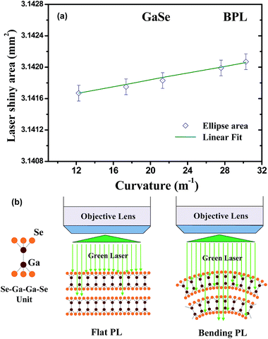
Finally, the mechanism of PL enhancement under upward bending of the layered GaSe is analyzed and discussed. Fig. 4(b) clearly reveals that the analysis of overall intensity change vs. curvature is a relation containing linear term and square term as I(x) = (0.288 ± 0.012) + (0.017 ± 0.003 m)x + [(2.95 ± 1.05) × 10−4 m2]x2, where x is the curvature of bending (m−1). The linear-term change of BPL intensity may directly relate to the shiny-area change of laser illumination while the square-term alteration is caused by bond-angle widening under upward bending. Fig. 6(a) shows the calculated shiny area of laser (mm2) as a function of curvature from R−1 = 12.265 to 30.276 (m−1) using the calculation of previous equations. It is obvious that the shiny area increased linearly with the curvature is increased, following a relation of A(x) = (3.1415 ± 0.0001) + [(2.2 ± 0.4) × 10−5 m]x (mm2), shown by the solid line in Fig. 6(a). For the non-linear (square) term related PL change, the luminescence efficiency of BPL is also enhanced owing to the widening of emission solid angle of each Se–Ga–Ga–Se unit in the GaSe under laser shiny as compared to that of the flat PL condition. The representative scheme for indicating the difference is depicted in Fig. 6(b) for comparison. The direct bandgap emission of P1 peak of GaSe may originate from the in-plane Ga–Se bond with a recombination from Ga 4s* antibonding state (EC) to Se 4p bonding state (EV).25 As shown in Fig. 6(b), when the incident laser light shines on the sample and all scattered lights are collected by the object lens in the micro-PL system, the bent GaSe monolayers reveal more widening to acceptance solid angle as well as much deeper light transmission in the layers for rendering more enhanced PL emission. It is noticed that the absorption coefficient of GaSe is about α ≈ 7048 cm−1 at 532 nm (laser wavelength) determined by transmittance measurement. The penetration depth δ of the layered flat GaSe at 532 nm can be δ = 1/α, ∼1.42 μm. For a upward bent GaSe with the thickness of t ≈ 30 μm (see Fig. 1(b)), the upper out-side layer surfaces (>t/2 part) would suffer extension (tensile) strain whereas the inner (<t/2 part) layered planes could be compressive such as the formation of nanotube GaSe of different thicknesses.26 The middle layer (=t/2) of the GaSe should be neutral and unstrained. Because the penetration depth δ is much lower than the sample thickness t, the outer-layers GaSe has suffered an in-plane tensile strain to the Ga–Se bond, the peak energy of the bandgap emission is thus redshifted. In the BPL experiments, the test GaSe sample is not being thinly exfoliated to few layer. The experimental design is necessary to reach high accumulation of illumination intensity for achieving high measurement accuracy in the BPL study. The analyses of PL enhancement, bandgap shift, and lattice-constant change in the layered GaSe with upward bending could be well referred in future flexible light-emitting-device application of 2D materials.
4. Conclusions
In conclusion, an accurate and adjustable bending steel holder was designed to study the curvature-dependent PL enhancement and bandgap shift of the layered GaSe 2D material at normally upward bending conditions. The designed holder can avoid layer wrinkles and stress non-uniformity of the layered sample under testing. With the curvature increased from R−1 = 0 (flat) to R−1 = 30.276 m−1, the normalized BPL intensities are enhanced by a relationship of I(x) = (0.288 ± 0.012) + (0.017 ± 0.003 m)x + [(2.95 ± 1.05) × 10−4 m2]x2, where x is the curvature (m−1). According to the detailed analysis and geometric calculation, the BPL enhancement can be attributed to two mechanisms: (1) linear change by mainly the laser-shiny-area increase, and (2) non-linear variation of increasing the acceptance solid angle from the Se–Ga–Ga–Se bond units under upward bending. When the curvature of the bent GaSe is increased, the PL main-peak energies are also redshifted (reduced). It is mainly owing to in-plane Ga–Se bond-length expansion caused by tensile strain. A further analyses of in-plane lattice constant a vs. bandgaps of the GaSe by taking into account those results of GaSe1−xSx (0.1 ≤ x ≤ 0.4) with similar structure has also been done. A referred expression of a(Eg) = a0 + a1Eg + a2Eg2 with a0 = 5.3167 Å, a1 = −1.3357 Å (eV)−1, and a2 = 0.27571 Å (eV)−2 can be obtained. This formula could be further referred in tuning bandgap and lattice constant for the bent GaSe light-emitting device in future flexible optoelectronics use.Conflicts of interest
The authors declare no conflicts of interest.Acknowledgements
This work was sponsored by the financial support from the Ministry of Science and Technology of Taiwan under the grant No. MOST 104-2112-M-011-002-MY3.Notes and references
- K. S. Novoselov, A. K. Geim, S. V. Morozov, D. Jiang, Y. Zhang and S. V. Dubonos, et al., Science, 2004, 306, 666–669 CrossRef PubMed.
- C. S. Jung, F. Shojaei, K. Park, J. Y. Oh, H. S. Im, D. M. Jang, J. Park and H. S. Kang, ACS Nano, 2015, 9, 9585–9593 CrossRef CAS PubMed.
- Y. Ni, H. Wu, C. Huang, M. Mao, Z. Wang and X. Cheng, J. Cryst. Growth, 2013, 381, 10–14 CrossRef.
- X. Li, M.-W. Lin, J. Lin, B. Huang, A. A. Puretzky and C. Ma, et al., Sci. Adv., 2016, 2, e1501882 Search PubMed.
- M. Mahjouri-Samani, M. Tian, K. Wang, A. Boulesbaa, C. M. Rouleau, A. A. Puretzky, M. A. McGuire, B. R. Srijanto and K. Xiao, et al., ACS Nano, 2014, 8, 11567–11575 CrossRef CAS PubMed.
- V. Capozzi and M. Montagna, Phys. Rev. B, 1989, 40, 3182–3190 CrossRef CAS.
- R. Sporken, R. Hafsi, F. Coletti, J. M. Debever, P. A. Thiry and A. Chevy, Phys. Rev. B, 1994, 49, 11093–11099 CrossRef.
- E. Aulich, J. L. Brebner and E. Mooser, Phys. Status Solidi, 1969, 31, 129–131 CrossRef CAS.
- C. S. Jung, K. Park, F. Shojaei, J. Y. Oh, H. S. Im, J. A. Lee, D. M. Jang, J. Park, N. S. Myoung, C.-L. Lee, J. W. Lee, J. K. Song and H. S. Kang, Chem. Mater., 2016, 28, 5811–5820 CrossRef CAS.
- S. Schwarz, S. Dufferwiel, P. M. Walker, F. Wither, A. A. P. Trichet, M. Sich, F. Li, E. A. Chekhovich, D. N. Borisenko and N. N. Kolesnikov, et al., Nano Lett., 2014, 14, 7003–7008 CrossRef PubMed.
- Y. P. Varshni, Physica, 1967, 34, 149–154 CrossRef CAS.
- E. Scalise, M. Houssa, G. Pourtois, V. Afanas'ev and A. Stesmans, Nano Res., 2011, 5, 43–48 CrossRef.
- Y. Chen, J. Xi, D. O. Dumcenco, Z. Liu, K. Suenaga and D. Wang, et al., ACS Nano, 2013, 7, 4610–4616 CrossRef CAS PubMed.
- J. Quereda, R. Biele, G. Rubio-Bollinger, N. Agraït, R. D'Agosta and A. Castellanos-Gomez, Adv. Opt. Mater., 2016, 4, 1939–1943 CrossRef.
- Y. Zhang, T.-T. Tang, C. Girit, Z. Hao, M. C. Martin and A. Zettl, et al., Nature, 2009, 459, 820–823 CrossRef CAS PubMed.
- J. Kim, S. S. Baik, S. H. Ryu, Y. Sohn, S. Park and B.-G. Park, et al., Science, 2015, 349, 723–726 CrossRef PubMed.
- S. Cao, J. Zhao, W. Yang, C. Li and J. Zheng, J. Mater. Chem. C, 2015, 3, 8844–8851 RSC.
- C. H. Ho, S. T. Wang, Y. S. Huang and K. K. Tiong, J. Mater. Sci.: Mater. Electron., 2009, 20, 207–210 CrossRef CAS.
- C. H. Ho and Y. J. Chu, Adv. Opt. Mater., 2015, 3, 1750–1758 CrossRef.
- Y. Wu, H. R. Fuh, D. Zhang, C. Ó. Coileáin, H. Xu, J. Cho, M. Choi, B. S. Chun, X. Jiang and M. Abid, et al., Nano Energy, 2017, 32, 157–164 CrossRef CAS.
- C. C. Wu, C. H. Ho, W. T. Shen, Z. H. Cheng, Y. S. Huang and K. K. Tiong, Mater. Chem. Phys., 2004, 88, 313–317 CrossRef CAS.
- C. H. Ho, C. C. Wu and Z. H. Cheng, J. Cryst. Growth, 2005, 279, 321–328 CrossRef CAS.
- X. Li, L. Basile, B. Huang, C. Ma, J. Lee, I. V. Vlassiouk, A. A. Puretzky, M. W. Lin, M. Yoon and M. Chi, et al., ACS Nano, 2015, 9, 8078–8088 CrossRef PubMed.
- W. Jie, X. Chen, D. Li, L. Xie, Y. Y. Hui, S. P. Lau, X. Cui and J. Hao, Angew. Chem., 2015, 127, 1201–1205 CrossRef.
- M. O. D. Carmara, A. Mauger and I. Devos, Phys. Rev. B, 2002, 65, 125206 CrossRef.
- M. Côté and M. L. Cohen, Phys. Rev. B, 1998, 58, R4277–R4280 CrossRef.
Footnote |
| † Electronic supplementary information (ESI) available. See DOI: 10.1039/c7ra11600d |
| This journal is © The Royal Society of Chemistry 2018 |

