 Open Access Article
An ultra-compact blackbody using electrophoretic deposited carbon nanotube films
Albert Lin *,
Chien-Chih Yang,
Parag Parashar,
Chien-Yung Lin,
Ding Rung Jian,
Wei-Ming Huang,
Yi-Wen Huang,
Sze Ming Fu,
Yan Kai Zhong and
Tseung Yuen Tseng*
Department of Electronics Engineering, National Chiao-Tung University, Hsinchu, Taiwan 30010. E-mail: hdtd5746@gmail.com.tw; tseng@cc.nctu.edu.tw
First published on 17th January 2018
Abstract
Carbon nanotubes (CNTs) possesses decent optical properties and thus can be considered as a candidate for perfect absorbers due to their close-to-air refractive index and minimal extinction. However, weak absorption in porous materials, due to the low extinction coefficients, requires an inevitably thick absorption layer (∼100 μm) for the perfect opaque absorbers. Thus, the requirement of large thicknesses of CNTs prohibits them from being used as miniaturized integrated photonic devices. Here, we propose an electrophoretic deposited (EPD) CNT resonant cavity structure on tantalum (Ta) to enhance optical absorption. Efficient random light scattering along with the resonant cavity structure using Ti/SiO2 stacking enhances the absorption in our proposed EPD-CNT film while maintaining the total device thickness to <1 μm. The experiment results reveal that the absorption band covers the entire UV-VIS-NIR spectrum (λ = 0.3–2.6 μm), using resonant-cavity EPD-CNT design. The EPD deposition process is done at relatively low temperature < 120 °C. We believe that this proposal is very promising for sensing, antenna, and thermophotovoltaics (TPV), in terms of bandwidth, compactness and cost.
Introduction
In recent years, the studies of metamaterial perfect absorbers have been widely conducted because of their versatile applications in sensing, antenna, and thermophotovoltaics (TPV).1–5 There have been many research studies to fulfill the concepts of the broadband absorption using nano-photonic metamaterial perfect absorbers (MPA's), and there have been many efforts reported to date.6–15 Among these efforts, Fang et al.,14 proposed a hyperbolic metamaterial (HMM) tapered structure that included layer-by-layer metal-dielectric tapered structure to achieve a broad absorption band. The incident photons are absorbed by various portions of the HMM metal-dielectric stacking where the coupling of photons to the metallic films is from the side of the HMM nano-cones. Alu et al.16 proposed the use of Au metallic nano-cones in order to facilitate enhanced absorption. The metallic conical structure exploited the combination of two non-resonant effects, i.e. plasmonic brewster light funneling and adiabatic plasmonic focusing.In most works of nano-photonics MPAs, metals are usually selected as the absorbing materials owing to their high extinction coefficients over a wide spectral range. Essentially for metallic MPAs, the thickness of the metallic absorption layers is not required to be thick. For UV-VIS-NIR ranges, several micrometers in thickness are enough to fully absorb the incoming photons due to the high extinction coefficients of the metallic materials. However, the problem associated with the metallic MPAs is that the coupling of the incoming photons with the metallic layers can be difficult because of the significant refractive index difference between the metals and the ambience. Owing to this reason different schemes have been proposed in recent years to increase the photon coupling and photon confinement inside the metallic or metal-dielectric nanostructures, in order to achieve a perfect blackbody absorption over a broad spectral range. These include adiabatic coupling,14–16 plasmonics,10 hyperbolic dispersion,14 and field penetration17 phenomenon. Nonetheless, extensive use of lithography and etching processes also impose an extra cost and time inefficiency in most of these structures.
In contrast to metal-dielectric nano-photonic perfect absorbers, porous materials present another route for high absorption. Porous materials have close-to-unity real refractive index, and therefore, the in-coupling of the photons into the porous materials is not an issue due to their close-to-air refractive indices. As far as porous materials are concerned, CNTs has a higher melting point, higher mechanical and tensile strength than other noteworthy porous metal oxides such as NiO, Fe2O3, Co3O4, Mn2O3, NiFe2O4, and aluminum oxide,18 thereby, suitable for high temperature and harsh environment applications, such as thermophotovoltaics (TPV). Besides, efforts are being made in recent years to grow CNTs at a relatively low temperature (150 °C),19 as compared to high temperature CVD process, to lower the cost of CNT raw materials.
Inherent low extinction coefficient of CNT and other porous materials leads to a weak absorption and thus a large device thickness is required to achieve in the optical regime. Due to this constraint, CNTs are thus excluded from being categorized as an effective MPAs.6,20 Instead, CNTs are more often referred to as opaque materials rather than a photonic device. To achieve the high-absorption property, the required thickness of carbon nanotube absorber21–26 is usually about tens to hundreds of micrometers as discussed previously. Among these advancements, a 70 μm thick CNT grown on glass substrate with 1 nm Fe seed layer using 775 °C CVD is shown to achieve perfect blackbody.22 A forest of vertically aligned single-walled carbon nanotubes (SWNTs)23 behaves most similarly to a black body for the UV (200 nm) to far infrared (200 μm) regime. Besides, dark materials made by a low-density nanotube array26 also have been engineered to have an extremely low index of refraction together with the nanoscale surface roughness of the arrays to induce a nearly-perfect optical absorption material. The fact remains that a large thickness is required is a common problem when perfect absorbers are realized using highly porous materials to match the impedance of air. Due to the large thickness restraint of CNT absorbers, it can be hard to integrate the CNT absorbers with other nanoscale devices. Therefore, thickness minimization of CNT absorbers while maintaining their high absorption property is the key issue for the integration of CNTs with other optical devices. The recent work by N. Selvakumar et al.27 reports the 800 °C chemical vapor deposition (CVD) CNT on stainless steel substrate using tandem absorption of CNT and metallic substrate that reduced CNT thickness requirement to several micrometers. The decent absorption property achieved here27 with a reduced thickness is promising. But the extensive use of high processing temperature ∼800 °C prevents the use of flexible substrates along with the possible process integration with many low-temperature materials. Here, in the work proposed we use low-temperature < 120 °C electrophoretic deposition (EPD) to realize ultra-compact CNT absorbers with the aid of broadband resonant cavity design. EPD process is an economical and versatile processing technique for the carbon nanotubes (CNTs).28 Furthermore, no lithography and etching processes are required in our structure, thereby, adding cost and time efficiency to our device. The miniaturized dimension is <1 μm with broadband absorption over λ = 0.3 μm to λ = 2.6 μm.
Specifically, we present the process of EPD for fabricating carbon nanotubes, the UV-VIS-NIR and Fourier transform infrared spectroscopy (FTIR) measurement results, and the angular absorption measurement results. Also, we investigate the dependence of broadband absorption on the EPD CNT thickness. Finally, the ultimate purpose is to achieve reduced-thickness CNT absorbers with the aid of an optical broadband resonant cavity and the random light scattering within the EPD CNT films. With this low temperature processing together with the resonant cavity, our structure is very efficient in terms of bandwidth, compactness, and the integrability with other photonic devices.
Simulation
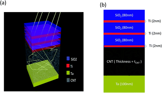
Simulation results have been presented in this section. The simulation software we used is Rsoft DiffractMOD™ and the absorption calculation is based on the rigorously coupled wave analysis (RCWA).The material parameters including refractive indices and extinction coefficients have been taken from Rsoft™ database,29 and the CNT refractive index is from a literature.22 Fig. 1 shows our proposed structure. The structure is a combination of CNTs and a resonant cavity consisting of a bottom Ta layer and alternating Ti/SiO2 layers. In principle, if we want to achieve full absorption of light, the thickness of CNTs must be tens to hundreds of micrometers due to their porous nature and the corresponding low absorption coefficients. Therefore, with the integration of resonant cavity, we try to reduce the thickness of CNT perfect absorbers. The thickness of CNTs in the simulation is 700 nm, and the cavity is composed of three pairs of alternating 2 nm Ti and 80 nm SiO2 thin films. The 100 nm Ta on the bottom serves as the bottom reflection layer to eliminate transmittance and also serves as the electrode during EPD.
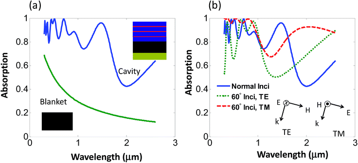
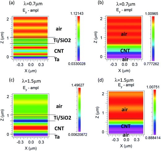
Fig. 2 illustrates the light paths for the standalone CNT blanket and the CNTs with a resonant cavity. A significant portion of photons can penetrate standalone CNTs while photons can be fully absorbed by CNTs due to the confinement achieved by the resonant cavity. The simulation results in Fig. 3 demonstrate this phenomenon. The absorption of CNTs with a cavity is much higher than the blanket of standalone CNTs over the entire broadband wavelength range from λ = 300 nm to λ = 2600 nm. The oscillations in the absorption are due to the fact that the resonance phenomenon is very pronounced in the cavity structure. Fig. 3(b) further shows the omnidirectional property of the structure where the absorption of 60° incidence at TE and TM polarizations is not decreased over the same broad spectral range λ = 300 nm to λ = 2600 nm as compared to the normal incidence. It should be noted that the refractive index of the CNTs is assumed to be 1.02 + 0.04i.22 Thus, it is a porous and weak absorption material that has been employed in the simulations. The absorption enhancement due to the random light scattering in EPD-CNTs has not been reflected in this section since the highly random, highly entangled EPD-CNT structure is not in fact computationally manageable. As a result, the experimental absorption can be even superior in terms of absorption perfection and bandwidth, compared to the simulation results. The field profiles are presented in Fig. 4. It can be clearly seen that the electromagnetic field is effectively confined in CNTs with the resonant cavity design. Without the Ta and Ti/SiO2 resonant cavity, the electromagnetic field directly penetrates the standalone blanket of CNTs since 700 nm CNTs are not thick enough to fully absorb the incident fields, as evident from Fig. 4(b) and (d). As a result, with the integration of the resonant cavity to the structure, the thickness of CNT absorbers can be minimized to several hundred nanometers. It will be clear later in the Experimental section that with the aid of random light scattering in EPD-CNTs, the measured absorption of a thin EPD-CNT device can be increased further from the simulated values.
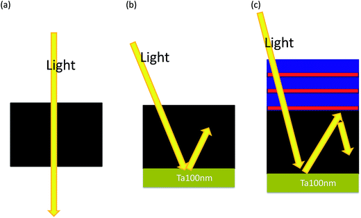 | ||
| Fig. 2 (a) The light path in blanket CNTs, (b) CNTs with a backside Ta reflection layer, and (c) CNTs with a resonant cavity. | ||
Experiment
In this section, we present the experimental results for the proposed cavity-type EPD-CNT structure. Since the thickness of CNT films has to be confirmed, we measure the thickness dimensions by scanning electron microscope (SEM). Fig. 5(a) is the SEM micrographs of the films, and Fig. 5(b) is the Raman spectroscopy. Various thicknesses of CNT-EPD films are deposited on Ta substrate in this work. Fig. 5(a) also shows the zoom-in micrograph of the CNTs cross-section to show the randomly distributed nature of EPD-CNTs. In addition, random distribution of CNTs is also evident in the top view, therefore, supports our discussion that the enhanced broadband absorption is in part due to the random light scattering within EPD-CNTs. In the Raman spectroscopy, we observe the G and D band signal. The G-band (∼1582 cm−1) is the primary Raman active mode in graphite, and it provides evidence of the sp2 bonded carbon existing in planar sheet configurations. Thus, the G band signal indicates that the sample can be graphite, graphene, or CNT since all of them have the sp2 bonded carbon in the benzene structure. The D-band (∼1350 cm−1), known as the disorder or defect mode, originates from the edge configurations in graphene where the planar sheet configuration is disrupted. The mode is exhibited on the edge of graphene sheet or the open end of a carbon nanotube, where defects exist.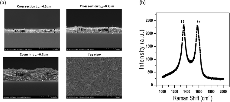 | ||
| Fig. 5 (a) SEM micrographs of the EPD-CNT films in this experiment. The CNT films are deposited on a Ta bottom layer with various thickness. (b) Raman spectroscopy of the EPD-CNT film. | ||
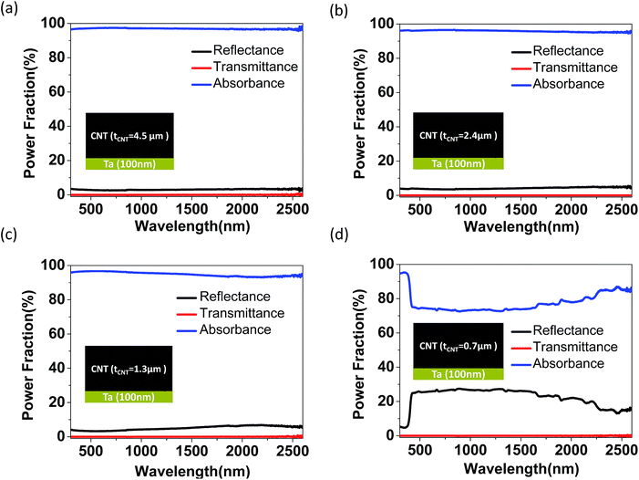
Fig. 6 and 7 show the data of measurements, including the reflectance (R), the transmittance (T), and the absorption (A). The detailed measurement drawing can be referred from our past publication.30 Fig. 6 shows the measured results of EPD-CNT films on a 100 nm Ta layer. The broadband spectral absorption is quite high in the range of λ = 300–2600 nm for tCNT = 4.5 μm and 2.4 μm. Although the resonant cavity has not been formed, the Ta back reflection layer and the random distribution nature of EPD-CNTs have already effectively increased the absorption. The averaged absorption (Aavg) is 0.97 for EPD-CNTs (tCNT = 4.5 μm) with a Ta bottom layer in Fig. 6(a). A gradual decrease in absorption is observed with a decreased tCNT, and ∼0.8 absorption is observed for the case of tCNT = 0.7 μm in Fig. 6(d). Fig. 7 shows the spectral absorption for CNTs with cavity design consisting of a Ta bottom layer and 3-pair Ti/SiO2 top layers. Firstly, Fig. 7(b) depicts the UV-VIS-NIR absorption spectrum from λ = 300 nm to λ = 2600 nm. Fig. 7(c) further shows the FTIR result of 1 − Rspec − Tspec from λ = 1.2 μm to λ = 10 μm. Due to the planar geometry, 1 − Rspec − Tspec ≅ 1 − R − T = A (absorption). This point will be explained in more details in the method section. It can be extracted from Fig. 7(c) that with the cavity design and tCNT ∼ 500 nm, the high absorption exists from λ = 300 nm to λ = 4810 nm. After λ = 5 μm, the spectral absorption begins to decay due to the geometry of tCNT ∼ 500 nm and tSiO2 = 80 nm for this experiment. To realize devices with a larger bandwidth or operation in longer wavelength regimes, increasing tCNT and tSiO2 can certainly be effective. It is worth to mention that the absorption and bandwidth in the experiment are further improved as compared to the simulation results mentioned in the previous section. The reason is that the CNTs in the simulation are assumed to be vertically aligned with refractive index 1.02 + 0.04i,22 but the CNTs deposited by EPD are randomly distributed. These entangled EPD-CNTs increase the probability of random light scattering in the CNT films, and thus absorption can be increased accordingly. This point has been evident from many solar cell light trapping literature.31–37 In short, the experimental results verify the proposed design, i.e., we can reduce the thickness of CNT absorbers by incorporating light scattering phenomenon in EPD-CNTs and a resonant cavity design using top Ti/SiO2 layers and the bottom Ta layer.
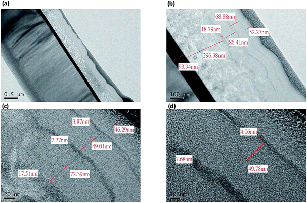
Further material analysis is conducted to investigate the device structure and layer deposition in the cavity type CNTs with 100 nm-Ta and 3-pair 3 nm-Ti/80 nm-SiO2 cladding. Fig. 8 demonstrates the STEM cross-section image of the fabricated device. The thickness of the EPD-CNT layer, in this case, is ∼500 nm. The thickness variation is minimized by using a centrifuge to uniformly disperse the CNTs in the mixture of nitric and sulphuric acids (HNO3 and H2SO4) solution although some layer thickness variation is still observed here. The thickness variation in CNT films is due to the EPD solution process, and the roughness and porosity of the CNT film can affect the morphology, uniformity, and the porosity of the subsequent SiO2 and Ti films. Further reduction in surface roughness and morphology is desired but it should be emphasized that the low-temperature chemical solution processing inevitably leads to surface morphology not comparable to vacuum deposition, and the surface roughness of the EPD-CNT films here is comparable to other EPD CNT works in literature.38 In Fig. 8(c) and (d), it is observed that although as-deposited thickness of Ti thin film is ∼3 nm, diffusion of Ti into SiO2 or CNT inevitably exists. This is due to the fact that the EPD-CNT film is highly texturized and porous with thickness non-uniformity as evident from Fig. 5, and this makes the SiO2 layer above less dense. From optics viewpoint, the slight mix-up of Ti and SiO2 layer is not detrimental as long as the dimension of the diffused Ti film is still much smaller than the photon wavelength. This is the essence of effective index theory in optics.39,40
Conclusions
In this work, we propose an ultra-compact ultra-broadband ideal blackbody composed of a Ta bottom layer, EPD-CNTs, and alternating Ti/SiO2 layers. In the past, due to the hollow-cylindrical-shell structure of CNTs, the light coupling into the CNTs is extremely simple, similar to other porous materials. However, owing to the low material density and volume ratio, the thickness of most CNT perfect blackbody in literature is usually in the range of 10–100 μm (ref. 21–26) to achieve high absorption. As a result, although the high absorption property is fulfilled, the large thickness of CNT obstructs the integration of CNTs with other miniaturized optical devices. Here, we propose a thin CNT perfect absorber using EPD-CNTs with resonant cavity design consisting of alternating metal-dielectric layers. The simulation reveals that the resonances can be supported by the proposed structure where the EPD-CNT film is sandwiched between Ti/SiO2 multilayers and the bottom Ta reflector. From the experimental results, it is evident that the proposed cavity-type EPD-CNT structure can indeed achieve high absorption from λ = 300 nm to λ = 2600 nm while the thickness of the EPD-CNT layer is only ∼500 nm, and the total device thickness is <1 μm. The broadband high absorption of thin EPD-CNT absorbers is attributed to the random orientation of the EPD-CNTs during EPD, which enhances light scattering and absorption. This aspect is quite different from many CNT perfect blackbodies in literature where vertically aligned CNTs are frequently used.21–26 In addition, the proper cavity design leads to enhanced photon confinement over a very broad bandwidth. We believe that this proposal constitutes the most promising CNT blackbody design due to a wide band absorption that could be achieved by employing a thin CNT layer. Also, the miniaturization of the CNT thickness and low-temperature processing enables its integration with other optical devices and makes it possible for CNTs to be categorized as a metamaterial perfect absorber (MPA) with dimension comparable to photon wavelengths.Methods
Sample fabrication
The method we used to fabricate the carbon nanotubes (CNTs) film is electrophoretic deposition (EPD). The EPD is an economical method that only requires simple equipment and can be completed at low temperature (<120°), and thus it is commonly employed in the fabrication of films from colloidal suspensions. The EPD is essentially composed of two steps. The first step is suspending CNTs in a liquid and applying a voltage to force CNTs moving toward the electrode. In the second step, the nanoparticles coagulate at the electrode and form a coherent coating of CNTs. Initially, we disperse 1 g CNTs in a 40 mL mixture of nitric and sulphuric acids (HNO3 and H2SO4). The volumetric proportion of nitric acids to sulphuric acids is 1![[thin space (1/6-em)]](https://www.rsc.org/images/entities/char_2009.gif) :
:![[thin space (1/6-em)]](https://www.rsc.org/images/entities/char_2009.gif) 3. Therefore, the volume of the nitric acid is 10 mL, and the volume of the sulphuric acid is 30 mL. The purpose of this step is to purify and to disperse the as-produced CNTs since they are usually entangled or aggregated and are full of impurities. Afterward, we heat up the solution on a hot plate at 120 °C for 30 minutes, and the solution is rinsed with deionized water until the pH value is ∼7. The excess water is then evaporated in an oven at 80 °C for ten hours. After purification, we can acquire 0.5 g CNTs. i.e., the production is ∼50%. Subsequently, we triturate 0.03 g after-processing CNTs and pour the powders into 60 mL isopropyl alcohol and 0.4 mL HCl to prepare the CNT suspensions for EPD. The CNT suspensions are sonicated in an ultrasonic bath for 2 hours to have well-dispersed suspensions before EPD. Ta/Si is used as the cathode during EPD, and we have deposited 100 nm Ta on a silicon wafer previously using an ULVAC™ ENTRON W200 sputter. The anode is stainless steel. Next, we apply an electric field between these two electrodes, and the nanotubes will aggregate at the cathode to form a CNT film. The CNT film is then baked at 60 °C in oven for 5 minutes. After the deposition of CNTs has been finished, we deposit Ti/SiO2 alternating layers by electron-gun (e-gun) evaporator AST PEVA 600I. The pressure is kept <3 × 10⁻⁶ torr for Ti deposition and <5 × 10⁻⁶ torr for SiO2 deposition. We deposit ∼3 nm Ti on the top of CNTs and then deposit 80 nm SiO2 on Ti. The process is repeated until three pairs of alternating layers have been fabricated. The EPD-CNT film is highly texturized and porous, and thus makes the 80 nm SiO2 layer above less dense. The as-deposited thickness of Ti thin film is ∼3 nm, but because Ti is deposited on the less dense SiO2 layers or the porous CNT film, some diffusion of Ti into SiO2 or CNT inevitably exists.
3. Therefore, the volume of the nitric acid is 10 mL, and the volume of the sulphuric acid is 30 mL. The purpose of this step is to purify and to disperse the as-produced CNTs since they are usually entangled or aggregated and are full of impurities. Afterward, we heat up the solution on a hot plate at 120 °C for 30 minutes, and the solution is rinsed with deionized water until the pH value is ∼7. The excess water is then evaporated in an oven at 80 °C for ten hours. After purification, we can acquire 0.5 g CNTs. i.e., the production is ∼50%. Subsequently, we triturate 0.03 g after-processing CNTs and pour the powders into 60 mL isopropyl alcohol and 0.4 mL HCl to prepare the CNT suspensions for EPD. The CNT suspensions are sonicated in an ultrasonic bath for 2 hours to have well-dispersed suspensions before EPD. Ta/Si is used as the cathode during EPD, and we have deposited 100 nm Ta on a silicon wafer previously using an ULVAC™ ENTRON W200 sputter. The anode is stainless steel. Next, we apply an electric field between these two electrodes, and the nanotubes will aggregate at the cathode to form a CNT film. The CNT film is then baked at 60 °C in oven for 5 minutes. After the deposition of CNTs has been finished, we deposit Ti/SiO2 alternating layers by electron-gun (e-gun) evaporator AST PEVA 600I. The pressure is kept <3 × 10⁻⁶ torr for Ti deposition and <5 × 10⁻⁶ torr for SiO2 deposition. We deposit ∼3 nm Ti on the top of CNTs and then deposit 80 nm SiO2 on Ti. The process is repeated until three pairs of alternating layers have been fabricated. The EPD-CNT film is highly texturized and porous, and thus makes the 80 nm SiO2 layer above less dense. The as-deposited thickness of Ti thin film is ∼3 nm, but because Ti is deposited on the less dense SiO2 layers or the porous CNT film, some diffusion of Ti into SiO2 or CNT inevitably exists.
Sample measurements
In this work, the reflectance (R), transmittance (T), and absorption (A) refer to total reflectance, total transmittance, and total absorption. Thus, in some places, the term “total” is not written out explicitly for succinct labeling. On the other hand, specular reflectance (Rspec) and specular transmittance (Tspec) means the optical power that can be collected by the numerical aperture (NA) of the lens/mirrors set of the equipment in the case where no integration sphere is present. Normally Rspec and Tspec are the power enclosed in a solid angle around the reflection line where the solid angle is determined by the numerical aperture (NA).The measurement of UV-VIS-NIR absorption spectrum is by measuring the reflectance (R) and the transmittance (T). The absorption (A) is then calculated by A = 1 − R − T. The integration sphere collects all diffracted power so the total reflectance (R), total transmittance (T), and total absorption (A) can be measured at normal incidence. Hitachi U-4100 is used where the light source is a quickly mountable type deuterium lamp for the ultraviolet region and a 50 W halogen lamp for the visible-near-infrared region. The pre-monochromator is Littrow monochromator using a diffraction grating, and the main monochromator is also of the grating type with two switchable diffraction gratings. The detector is photomultiplier for the UV-VIS region and a cooling type PbS photoconductive detector for the NIR region.
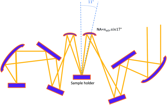
The Fourier transform infrared (FTIR) spectroscopy is used for λ = 1.2 μm to λ = 10 μm. Bruker IFS 66v/S Fourier transform infrared spectroscopy (FTIR) is used. The resolution is 0.25 cm−1. The light source is silicon carbide (SiC) glow bar, and the detector is a pyroelectric detector using deuterated lanthanum α alanine doped triglycine sulphate (DLATGS) with KBr window. In our FTIR measurement using Bruker machine, the incidence angle is the nearly-normal direction at 11 degrees (11°). Using e-gun evaporation or other low-cost deposition techniques such as sputtering, solution processes, and inkjet printing, is promising for MWIR/LWIR perfect absorbers because the surface roughness is a less severe concern for MWIR/LWIR regime. This is due to the large MWIR/LWIR wavelength dimension compared to the vertical/lateral sample surface roughness in the range of nanometers. As a result, the incident photons essentially cannot perceive the surface texture of the films. The fact of no need for MBE or ALD in the planar MWIR/LWIR perfect absorber structure here enhances its practicability for MWIR/LWIR applications. The setup for the FTIR measurement is shown in Fig. 9. In most FTIR machines there is not integration sphere, due to the long wavelength radiation is more robust to surface roughness. Since there is no integration sphere in FTIR machine, Rspec and Tspec are measured. Due to the fact that our structure is a planar structure and the fact that the Bruker™ FTIR has NA = sin![[thin space (1/6-em)]](https://www.rsc.org/images/entities/char_2009.gif) 15°, Rspec and Tspec are close to R and T, and thus 1 − Rspec − Tspec ≅ 1 − R − T = A. We have verified that the diffraction and light scattering from a 700 nm EPD CNT film are fully within 10° for UV-VIS-NIR (λ = 300–2600 nm), and this means the 1 − Rspec − Tspec is exactly the same as 1 − R − T = A for this wavelength regime in our FTIR measurement. Further increase in wavelength is unlikely to increase the light scattering angle due to the fact that the surface profiling and thickness variation is <50 nm from the SEM micrographs shown previously, and this dimension is insufficient to cause significant far-field light diffraction or scattering for wavelengths beyond UV-VIS-IR. As a result, the value of 1 − Rspec − Tspec can be used to infer the absorption behaviour of the sample in our case.
15°, Rspec and Tspec are close to R and T, and thus 1 − Rspec − Tspec ≅ 1 − R − T = A. We have verified that the diffraction and light scattering from a 700 nm EPD CNT film are fully within 10° for UV-VIS-NIR (λ = 300–2600 nm), and this means the 1 − Rspec − Tspec is exactly the same as 1 − R − T = A for this wavelength regime in our FTIR measurement. Further increase in wavelength is unlikely to increase the light scattering angle due to the fact that the surface profiling and thickness variation is <50 nm from the SEM micrographs shown previously, and this dimension is insufficient to cause significant far-field light diffraction or scattering for wavelengths beyond UV-VIS-IR. As a result, the value of 1 − Rspec − Tspec can be used to infer the absorption behaviour of the sample in our case.
Conflicts of interest
The authors declare no competing financial interests.Acknowledgements
We acknowledge the support for this work from the Ministry of Science and Technology (MOST), Taiwan under grant number MOST 104-2221-E-009-115-MY2.References
- N. Liu, M. Mesch, T. Weiss, M. Hentschel and H. Giessen, Nano Lett., 2010, 10, 2342–2348 CrossRef CAS PubMed.
- H.-T. Chen, W. J. Padilla, M. J. Cich, A. K. Azad, R. D. Averitt and A. J. Taylor, Nat. Photonics, 2009, 3, 148–151 CrossRef CAS.
- D. Dregely, R. Taubert, J. Dorfmüller, R. Vogelgesang, K. Kern and H. Giessen, Nat. Commun., 2010, 2, 267 CrossRef PubMed.
- X. Liu, T. Tyler, T. Starr, A. F. Starr, N. M. Jokerst and W. J. Padilla, Phys. Rev. Lett., 2011, 107, 045901 CrossRef PubMed.
- C. Wu, B. Neuner, J. John, A. Milder, B. Zollars, S. Savoy and G. Shvets, J. Opt., 2012, 14, 024005 CrossRef.
- C. M. Watts, X. Liu and W. J. Padilla, Adv. Opt. Mater., 2012, 24, OP98–OP120 CAS.
- H. Tao, N. I. Landy, C. M. Bingham, X. Zhang, R. D. Averitt and W. J. Padilla, Opt. Express, 2008, 16, 7181–7188 CrossRef PubMed.
- X. Liu, T. Starr, A. F. Starr and W. J. Padilla, Phys. Rev. Lett., 2010, 104, 207403 CrossRef PubMed.
- Y. Avitzour, Y. A. Urzhumov and G. Shvets, Phys. Rev. B: Condens. Matter Mater. Phys., 2008, 79, 045131 CrossRef.
- K. Aydin, V. E. Ferry, R. M. Briggs and H. A. Atwater, Nat. Commun., 2011, 2, 517 CrossRef PubMed.
- H. Tao, C. M. Bingham, A. C. Strikwerda, D. Pilon, D. Shrekenhamer, N. I. Landy, K. Fan, X. Zhang, W. J. Padilla and R. D. Averitt, Phys. Rev. B: Condens. Matter Mater. Phys., 2008, 78, 241103 CrossRef.
- H. Tao, C. M. Bingham, D. Pilon, K. Fan, A. C. Strikwerda, D. Shrekenhamer, W. J. Padilla, X. Zhang and R. D. Averitt, J. Phys. D: Appl. Phys., 2010, 43, 225102 CrossRef.
- J. Hao, J. Wang, X. Liu, W. J. Padilla, L. Zhou and M. Qiu, Appl. Phys. Lett., 2010, 96, 251104 CrossRef.
- Y. Cui, K. H. Fung, J. Xu, H. Ma, Y. Jin, S. He and N. X. Fang, Nano Lett., 2012, 12, 1443–1447 CrossRef CAS PubMed.
- D. Ji, H. Song, X. Zeng, H. Hu, K. Liu, N. Zhang and Q. Gan, Sci. Rep., 2014, 4, 4498 CrossRef PubMed.
- C. Argyropoulos, K. Q. Le, N. Mattiucci, G. D'Aguanno and A. Alu, Phys. Rev. B: Condens. Matter Mater. Phys., 2013, 87, 205112 CrossRef.
- Y. K. Zhong, S. M. Fu, N. P. Ju, M. Tu, B. Chen and A. Lin, IEEE Photonics J., 2016, 8, 2200109 Search PubMed.
- M. Farhat, T.-C. Cheng, K. Q. Le, M. M.-C. Cheng, H. Bagci and P.-Y. Chen, Sci. Rep., 2016, 6, 19984 CrossRef CAS PubMed.
- E. Dervishi, A. R. Biris, J. A. Driver, F. Watanabe, S. Bourdo and A. S. Biris, J. Catal., 2013, 299, 307–315 CrossRef CAS.
- Y. Ra'di, C. R. Simovski and S. A. Tretyakov, Phys. Rev. Appl., 2015, 3, 037001 CrossRef.
- A. Lenert, D. M. Bierman, Y. Nam, W. R. Chan, I. Celanovic, M. Soljacic and E. N. Wang, Nat. Nanotechnol., 2014, 9, 126–130 CrossRef CAS PubMed.
- H. Shi, J. G. Ok, H. W. Baac and L. J. Guo, Appl. Phys. Lett., 2011, 99, 211103 CrossRef.
- K. Mizuno, J. Ishii, H. Kishida, Y. Hayamizu, S. Yasuda, D. N. Futaba, M. Yumura and K. Hata, Proc. Natl. Acad. Sci. U. S. A., 2009, 106, 6044–6047 CrossRef CAS PubMed.
- F. J. García-Vidal, J. M. Pitarke and J. B. Pendry, Phys. Rev. Lett., 1997, 78, 4289–4292 CrossRef.
- A. Cao, X. Zhang, C. Xu, B. Wei and D. Wu, Sol. Energy Mater. Sol. Cells, 2002, 70, 481–486 CrossRef CAS.
- Z.-P. Yang, L. Ci, J. A. Bur, S.-Y. Lin and P. M. Ajayan, Nano Lett., 2008, 8, 446–451 CrossRef CAS PubMed.
- N. Selvakumar, S. B. Krupanidhi and H. C. Barshilia, Adv. Mater., 2014, 26, 2552–2557 CrossRef CAS PubMed.
- A. R. Boccaccini, J. Cho, J. A. Roether, B. J. C. Thomas, E. Jane Minay and M. S. P. Shaffer, Carbon, 2006, 44, 3149–3160 CrossRef CAS.
- Rsoft, Rsoft CAD User Manual, Rsoft Design Group, New York, 8.2 edn, 2010 Search PubMed.
- Y. K. Zhong, Y.-C. Lai, M.-H. Tu, B.-R. Chen, S. M. Fu, P. Yu and A. Lin, Opt. Express, 2016, 24, A832–A845 CrossRef CAS PubMed.
- F. Pratesi, M. Burresi, F. Riboli, K. Vynck and D. S. Wiersma, Opt. Express, 2013, 21, A460–A468 CrossRef PubMed.
- E. R. Martins, J. Li, Y. Liu, V. Depauw, Z. Chen, J. Zhou and T. F. Krauss, Nat. Commun., 2013, 4, 2665 Search PubMed.
- M. Burresi, F. Pratesi, K. Vynck, M. Prasciolu, M. Tormen and D. S. Wiersma, Opt. Express, 2013, 21, A268 CrossRef PubMed.
- A. Bozzola, M. Liscidini and L. C. Andreani, Prog. Photovoltaics Res. Appl., 2014, 22(12), 1237–1245 CAS.
- X. Sheng, S. G. Johnson, J. Michel and L. C. Kimerling, Opt. Express, 2011, 19, A841–A850 CrossRef CAS PubMed.
- C. Lin and M. L. Povinelli, Opt. Express, 2011, 19, A1148–A1154 CrossRef CAS PubMed.
- A. Lin and J. D. Phillips, Sol. Energy Mater. Sol. Cells, 2008, 92, 1689–1696 CrossRef CAS.
- B. J. C. Thomas, A. R. Boccaccini and M. S. P. Shaffer, J. Am. Ceram. Soc., 2005, 88, 980–982 CrossRef CAS.
- S. L. Chuang, Physics of Photonic Devices (Wiley Series in Pure and Applied Optics), Wiley, New York, 2nd edn, 2009 Search PubMed.
- P. Bhattacharya, Semiconductor Optoelectronic Devices, 2nd edn, Prentice-Hall, Upper Saddle River, NJ, 2006 Search PubMed.
| This journal is © The Royal Society of Chemistry 2018 |

