 Open Access Article
ZnS coating for enhanced environmental stability and improved properties of ZnO thin films
Anna Baranowska-Korczyc *a,
Mikołaj Kościńskiab,
Emerson L. Coy
 a,
Bartosz F. Grześkowiaka,
Małgorzata Jasiurkowska-Delaporte
 ac,
Barbara Peplińskaa and
Stefan Jurga
 a
a
aNanoBioMedical Centre, Adam Mickiewicz University, Umultowska 85, PL-61614 Poznań, Poland. E-mail: akorczyc@chem.uw.edu.pl
bDepartment of Physics and Biophysics, Poznań University of Life Sciences, Wojska Polskiego 38/42, PL-60637 Poznań, Poland
cThe Henryk Niewodniczański Institute of Nuclear Physics, Polish Academy of Sciences, Radzikowskiego 152, 31-342 Kraków, Poland
First published on 6th July 2018
Abstract
Low environmental stability of ZnO nanostructures in hydrophilic systems is a crucial factor limiting their practical applications. ZnO nanomaterials need surface passivation with different water-insoluble compounds. This study describes a one-step passivation process of polycrystalline ZnO films with ZnS as a facile method of ZnO surface coating. A simple sulfidation reaction was carried out in gas-phase H2S and it resulted in formation of a ZnS thin layer on the ZnO surface. The ZnS layer not only inhibited the ZnO dissolving process in water but additionally improved its mechanical and electrical properties. After the passivation process, ZnO/ZnS films remained stable in water for over seven days. The electrical conductivity of the ZnO films increased about 500-fold as a result of surface defect passivation and the removal of oxygen molecules which can trap free carriers. The nanohardness and Young's modulus of the samples increased about 64% and 14%, respectively after the ZnS coating formation. Nanowear tests performed using nanoindentation methods revealed reduced values of surface displacements for the ZnO/ZnS system. Moreover, both ZnO and ZnO/ZnS films showed antimicrobial properties against Escherichia coli.
Introduction
ZnO thin films have been extensively studied and applied to a wide range of devices, such as transistors, light-emitting diodes, sensor, and biosensors.1,2 The major challenges faced in establishing ZnO films for practical use have been concerned with improving their physical properties by efficient surface modification. A ZnS coating prepared on ZnO nanolayers has attracted considerable interest in recent years due to combining the advantages offered by the II–VI semiconductors.3 ZnO is characterized by high electron mobility, high thermal conductivity and a high exciton binding energy of 60 meV at room temperature, as well as a number of effective methods which allow nanostructures to be synthesized with different dimensionalities.4,5 ZnS has good thermal, chemical and mechanical stability, excellent transport properties and surface polarity.6 ZnO and ZnS form type-II heterojunction band alignment with optoelectrical properties not normally associated with either nanomaterial present separately. ZnS is characterized by a wider band gap than ZnO, of about 3.67 eV compared to 3.37 eV.7 This higher value results in carrier separation: electrons are confined in ZnO, while holes are accumulated in ZnS. Moreover, after ZnO surface passivation by ZnS, shallow defects such as surface oxygen vacancies are removed, which significantly improves the optical and electrical properties of the material. The ZnS coating also protects the surface of ZnO against environmental influences. The oxygen molecules are able to interact with free electrons and do not modulate the level of free carriers in the nanostructures.Although there are many different methods of ZnO surface passivation by ZnS, most are carried out at high temperature and high pressure. The ZnS passivation layer formed at room temperature in a one-step process is more unique. In the traditional approaches, ZnO/ZnS films have been prepared by magnetron sputtering deposition,8 and powders by the microwave-assisted solvothermal method.9 Core/shell ZnO/ZnS nanowires have been obtained by sulfurizing ZnO nanowires using a vapor phase method under 23 torr and sulfur powder at a temperature of 190 °C.10 ZnO nanorods have been sulfided by Na2S aqueous solution or immersed in alcoholic solutions of 2 nm ZnS quantum dots.11 In other studies, ZnO nanofibers have been covered by a ZnS shell during a gas-phase sulfidation reaction with hydrogen sulfide12 and sputtered ZnO films have been coated or totally converted to ZnS films by a sulfidation process.13
Coating with ZnS results in significant changes in the physicochemical properties of the ZnO nanostructures. It has been observed that ZnO/ZnS nanotube arrays possess higher conductivity and better photoresponse than ZnO nanotube arrays due to the fact that the type-II band gap alignment in ZnO/ZnS facilitates the transfer of photoexcited electrons from the conduction band of ZnS to that of ZnO; the photoexcited holes in the ZnO valence band are injected to the valence band of ZnS.14 The ZnS/ZnO nanocomposite shows good H2 evolution activity and stability without any co-catalyst, and superior catalytic performance in sunlight-driven H2.15 It was also noted that ZnO/ZnS heterostructured nanorods exhibit much better performance in photocatalytic hydrogen evolution than ZnO and 1D ZnS nanorods.16 Similarly, ZnO/ZnS nanocable and nanotube arrays demonstrate much higher photodegradation efficiency than ZnO nanowire arrays,3 and ZnO/ZnS nanorods exhibit a specific capacitance of 217 mF cm−2 at 1 mA cm−2 which is superior to pure ZnO and ZnS nanostructures.17
The properties of the ZnO/ZnS type-II heterojunction enable the construction of various devices and broaden the range of applications for the two materials. High-performance broad ultraviolet photodetectors have been fabricated on ZnO/ZnS core/shell nanowires18 and flexible branched ZnS/ZnO nanofilms.7 A flexible robust sensor with ZnO/ZnS core–shell nanoarrays was constructed to detect Pb2+ ions for potential applications in environmental protection and pollutant surveillance.19 ZnO nanorods covered with ZnS shell showed improved photocatalytic activity for antibiotics degradation.20 The presence of sulfur on the nanomaterial surface can facilitate further biofunctionalization and the preparation of biodetectors such as protein sensors based on ZnO/ZnS nanofibers.12 In addition, an amperometric cholesterol biosensor has been constructed based on enzyme-immobilized microtubular ZnO@ZnS heterostructures.21
There is no doubt that the ZnO/ZnS heterostructure combines the advantageous properties of both nanomaterials. This issue has been addressed in many reports in recent years. However, there is still a huge demand for the simple methods of ZnO/ZnS type-II heterojunction formation.
In this report, we introduce a simple concept of one-step passivation process of ZnO nanolayer carried out in a gas-phase method. A facile sulfidation reaction results in the formation of thin chemically stable ZnS layer on ZnO surface. This concept can help to overcome problems related to practical applications of ZnO nanostructures, for example, solubility in biological liquids. The synthesized ZnO/ZnS film can potentially offer a multifunctional base for designing various devices due to the fact that ZnO passivation with ZnS provides a new system characterized by high stability in a hydrophilic environment as well as improved mechanical and electrical properties. Moreover, antibacterial properties of ZnO remain unchanged after ZnS passivation process and even slightly improved, which can enhance their future potential for biological and medical applications.
Experimental
Synthesis of ZnO and ZnO/ZnS nanolayers
The ZnO nanolayers were synthesized by a spin-coating process using an aqueous solution of poly(vinyl alcohol) (PVA, Mw of 72![[thin space (1/6-em)]](https://www.rsc.org/images/entities/char_2009.gif) 000 Da) and zinc acetate dihydrate. The PVA mixture was prepared in water at 7.7% wt concentration. Following this, 0.25 g of zinc acetate was added to 1.25 g of polymer. The homogenous solution was spin-coated at 3000 RPM for 30 s. The single nanolayer was synthesized from 50 μl of the solution using 10 mm × 10 mm silicon (Si) substrates. The nanolayers were calcined in air at 500 °C for two hours to obtain polycrystalline ZnO.22 The samples were also prepared on Si covered with 300 nm thick silicon dioxide (SiO2) layer and quartz glass for electrical and antimicrobial properties studies, respectively. Different substrates were applied due to the fact that ZnO crystal morphology was not affected by the substrate effect at the selected temperature of calcination.
000 Da) and zinc acetate dihydrate. The PVA mixture was prepared in water at 7.7% wt concentration. Following this, 0.25 g of zinc acetate was added to 1.25 g of polymer. The homogenous solution was spin-coated at 3000 RPM for 30 s. The single nanolayer was synthesized from 50 μl of the solution using 10 mm × 10 mm silicon (Si) substrates. The nanolayers were calcined in air at 500 °C for two hours to obtain polycrystalline ZnO.22 The samples were also prepared on Si covered with 300 nm thick silicon dioxide (SiO2) layer and quartz glass for electrical and antimicrobial properties studies, respectively. Different substrates were applied due to the fact that ZnO crystal morphology was not affected by the substrate effect at the selected temperature of calcination.
The ZnO nanolayers were placed into a hermetic chamber with a volume of 50 ml in the presence of 4 ml of 20% aqueous solution of (NH4)2S. The nanolayers were exposed to decomposition products of ammonium sulfide for three hours.23 The ZnS nanolayers were synthesized on the ZnO surfaces as a result of the sulfidation process. A detailed description of the synthesis of the ZnO and ZnO/ZnS nanolayers is given in our previous study.24
Characterization of the nanolayers
The topography and roughness of ZnO and ZnO/ZnS nanofilms were studied by Atomic Force Microscopy (AFM, Icon Bruker). AFM measurements were performed with tapping mode and MESP Brucker probes covered with a conductive alloy of cobalt and chromium (CoCr). The AFM measurements were performed at 0.2 Hz with 512 probe scans for a single image.The chemical composition of the nanofilms was investigated by Energy Dispersive X-ray spectroscopy (EDX, Jeol 7001TTLS). Structural characterization of the layers was performed by Glazing incident X-ray diffraction (GI-XRD) using a high-resolution powder diffractometer (X'pert3 -MRD, PANalytical) employing CuKα1 radiation; the incident angle was 2° and the diffractometer parameters were 45 kV and 45 mA. Fourier transform infrared spectroscopy (FTIR) and Raman spectroscopy were also used to analyze the structure of ZnO and ZnO/ZnS samples. The infrared spectra were recorded by a BRUKER Tensor 27 Fourier Transform Infrared (FTIR) spectrometer using a diamond Attenuated Total Reflection (ATR) accessory. FTIR absorption spectra were measured in the wavenumber range 400 to 3500 cm−1 with a resolution of 4 cm−1. The Raman spectra were examined using an inVia Ranishaw Raman Microscopy System (Ranishaw, Old Town, Wotton-under-Edge, UK). The excitation source was an Ar laser (488 nm). Each spectrum was collected with five accumulations in the wavenumber range of 200 to 800 cm−1.
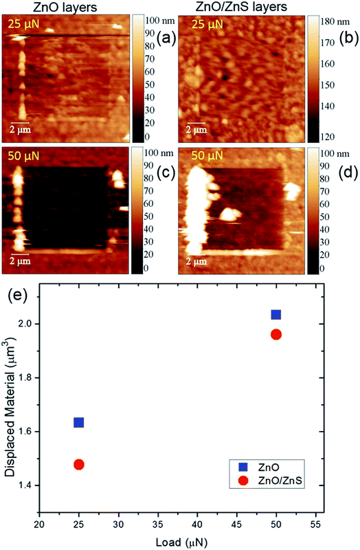
The nanohardness and elastic modulus of the samples were measured by nanoindentation (Hysitron TI 950 TriboIndenter) using a Berkovich diamond tip with a maximum penetration depth below 300 nm at room temperature. Hardness and elastic modulus values were determined from load–displacement curves by the Oliver–Pharr method.25 Samples were scanned under very low force settings to avoid displacements during the topographic survey. Nanowear tests were performed by holding a constant force of 25 and 50 μN and then calculating the displaced material by the residual imprint in Gwydion software.
In order to study the stability of the films before and after the sulfidation process, they were immersed in water for seven days. After ZnO nanofilm synthesis process, each sample was cut into four pieces. Two pieces were treated with H2S. As a result, two samples of ZnO and two samples of ZnO/ZnS nanofilms were obtained. One piece of ZnO sample and one with the ZnO/ZnS nanofilm were immersed in DI water for seven days, while the two remaining samples were not treated with any liquids (control samples). The dissolution process was observed using SEM (Scanning Electron Microscopy, Jeol 7001TTLS) images of each sample.
To study the electrical signal of the ZnO and ZnO/ZnS nanolayers, Conductive-AFM (C-AFM) analysis was performed using contact mode AFM (Bruker's INNOVA) and probes (SCM-PIC Bruker) covered with platinum and iridium alloy (Pt/Ir). During the measurement, a constant voltage of 0.5 V was applied to the layer. C-AFM signal was manually controlled by the Variable Gain Low Noise Current DLPCA-200 amplifier. The topography and C-AFM maps were scanned at the same time. The AFM measurements were obtained at a frequency of 0.1 Hz and 512 probe scans for each AFM image.
The electrical conductivity of the ZnO nanofilms before and after the sulfidation process was also measured using Van der Pauw method with a four-point probe placed at the corner of each sample. The measurements were performed using a Keithley 2400 source meter. The samples for C-AFM and conductivity measurements were prepared on 10 × 10 mm silicon substrates covered with a 300 nm silicon dioxide (SiO2) layer.
The antibacterial activities of the ZnO and ZnO/ZnS films against Escherichia coli (E. coli, DH5α) bacteria were studied using the antibacterial drop-test.26,27 The bacterial cells were cultured in 5 ml of Luria broth in a sterile 15 ml conical tube. The culture was incubated at 37 °C while being shaken at 220 RPM (MaxQ600 Shaker, Thermo Scientific) for 18–20 hours. The culture was then washed twice with sterilized saline (0.9% NaCl) solution by centrifuging at 4000 rpm for 10 minutes and then the cell pellet was re-suspended in sterilized saline solution. The samples were placed in Petri dish and 50 μl of 0.9% NaCl solution containing about 109 colony forming units (CFU) was added drop-wise onto the surface of a ZnO or ZnO/ZnS nanofilm synthesized on 10 × 10 mm quartz glass. Pure glass substrate without any film was used as a control sample. After four hours of incubation at RT, the samples were suspended in 3 ml of saline solution in 50 ml conical tubes and shaken at 300 RPM for 15 min. Serial dilutions were prepared by taking 100 μl of the previous solution and mixed with 900 μl of 0.9% NaCl. From this solution, 100 μl was plated onto the triplicate solid agar using the spread plate method. After incubation for 24 hours at 37 °C, the number of surviving bacterial colonies on the Petri dishes was counted and the survival ratio of bacteria was defined as the percentage of viable bacteria on the analyzed samples in comparison to a viable number of the bacteria on the control sample. Results are given as mean ± SD of triplicates from three separate experiments.
Results and discussion
Examination of the ZnO nanofilms before and after the sulfidation process reveal that they consist of crystals measuring tens of nanometers, which are visible by SEM (Fig. 1(a) and (b)) and AFM (Fig. 1(a) and (b)). The morphology of the layers does not change significantly after the formation of the ZnS coating due to the fact that the ZnS layer consists of sphalerite crystals measuring about 3 nm,24 and its thickness is in the range of 7 to 10 nm. The ZnS passivation film is formed in hydrogen sulfide (H2S) in gas phase, which resulted in the film closely following the morphology of the bottom layer. A very thin ZnS film is evenly synthesized on the top of ZnO layer due to the fact that each ZnO crystal is surrounded by H2S. The ZnS film does not affect the polycrystalline nature of the ZnO layer. The high surface area to volume ratio, which is a crucial element for realizing further applications and design nanodevices, remains unchanged.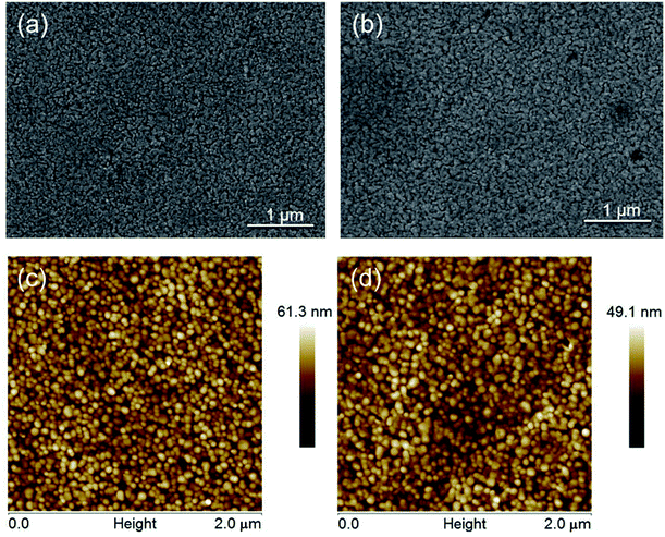 | ||
| Fig. 1 SEM images of (a) ZnO and (b) ZnO/ZnS nanofilms and AFM images of (c) ZnO and (d) ZnS/ZnS nanofilms. | ||
The roughness of the ZnO film does not change significantly during the sulfidation process. However, the ZnO nanolayer was found to have a higher roughness value than ZnO/ZnS (Table 1). The roughness decreases after the sulfidation process by the gaps between the crystals in the polycrystalline ZnO matrix being filled, which becomes slightly smoother (Table 1).
| ZnO film | ZnO/ZnS film | |
|---|---|---|
| Rq, square roughness (nm) | 6.54 | 5.98 |
| Ra, average deviation (nm) | 5.21 | 4.66 |
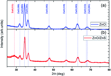
The X-ray diffraction patterns for samples of ZnO and ZnO/ZnS share the characteristic hexagonal wurtzite structure of ZnO (Fig. 2), according to the ICDD database (PDF: 04-003-2106). The ZnO/ZnS pattern contains an additional peak at 28.9 deg corresponding to the (111) lattice plane of cubic phase of ZnS (ICDS: 01-080-0020); this peak, the most intense in a typical X-ray diffraction pattern for cubic ZnS, indicates the nanocrystalline size nature of the ZnS top film. It has been noted previously for nanocrystalline grain-size ZnS thin films deposited by chemical bath28 and ZnS nanoparticles.29 The results are also consistent with our previous study,24 which indicates that the ZnS coating possesses a ZnS sphalerite structure with a 3 nm mean diameter of the crystals (Transmission Electron Microscopy, electron diffraction pattern). EDX examination revealed that the films consist of zinc and oxygen before the passivation process, the presence of sulfur was noted only for the ZnO/ZnS films.
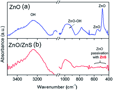
The infrared spectra of both ZnO and ZnO/ZnS films are presented in Fig. 3. The broad peaks at around 3200 cm−1 and 1000 cm−1 are attributed to OH and ZnO–OH vibration,30 respectively. The characteristic ZnO absorption bands were observed at around 550 cm−1 and 480 cm−1.31
It was found that the intensity of these bands decreased for ZnO nanoparticles covered partially with ZnS in comparison to pure ZnO nanostructures.30 These peaks are not found at the spectra of ZnO/ZnS nanolayers, indicating that the ZnS layer was successfully formed on the surface of ZnO, resulting in the extinguishing of the absorption bands related to ZnO vibration.
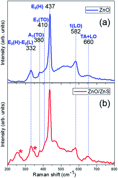
Fig. 4 shows the Raman spectra of ZnO and ZnO/ZnS films at an excitation wavelength of 488 nm in the 200 to 800 cm−1 spectral range. ZnO film (Fig. 4(a)) is characterized by the fundamental optical modes typical for wurtzite structure with C6v point group symmetry. The modes for ZnO before the sulfidation process are centered at around 332, 380, 411, 437, 582 and 660 cm−1, and are attributed to the processes E2(high) − E2(low), A1(TO), E1(TO), E2(high), 1LO and TA + LO, respectively.32 1LO mode corresponds to the superimposition of A1(LO) and E1(LO), which are characteristic of the presence of randomly-oriented ZnO crystals on the substrate.33 The strong peak at 437 cm−1 is associated with the high-frequency E2 mode of oxygen atoms and indicates a ZnO wurtzite hexagonal phase. The Raman spectrum of ZnO/ZnS nanofilm (Fig. 4(b)) reveals all the above mentioned modes characteristic of pure ZnO and additional modes related to the presence of a ZnS top layer. A large number of peaks are present in the range 200 to 350 cm−1 attributed to ZnS, including two modes of the first-order Raman frequencies characteristic of zinc blende, indicated in Fig. 4(b) as *, T2(TO) at 279 cm−1 and T2(LO) at 350 cm−1.34 The peaks at about 220 and 260 cm−1 are attributed to second-order Raman scattering.35 Moreover, the ZnO E2 mode is slightly shifted at 436 cm−1, indicating no significant tensile stress between the top sphalerite ZnS and bottom wurtzite ZnO layers. The vibrational modes for ZnO and ZnS observed simultaneously for films after the sulfidation process confirm the formation of ZnO/ZnS heterostructures.
To study the mechanical properties of the films before and after the passivation process, the values of the elastic modulus and hardness were determined using nanoindentation techniques. The Young's modulus values were estimated to be 72.40 and 82.36 GPa for ZnO film before and after the sulfidation process, respectively (Fig. 5(a)). The hardness scores of the sample before and after passivation were also measured, these were calculated as 1.1 GPa for ZnO alone and 1.8 GPa for the ZnO/ZnS nanolayer (Fig. 5(b)). The elastic modulus and hardness of the samples increased by 14% and 64% after ZnS coating, respectively. The nanoindentation tests for ZnO films deposited by a radio frequency magnetron sputtering system found Young's modulus to range from 68 to 125 GPa, similar to our results.36 However, the hardness was slightly higher for ZnO sputtered films, probably due to the differences in the route of synthesis, film morphology and shape of the crystal: i.e. cone-like rather than bead-like. It had also been found previously that crystal size influences the mechanical properties of ZnO materials. The hardness of a-plane ZnO thin films grew from 8.6 to 11.3 GPa as a result of increasing the grain size from 52 to 84 nm.37
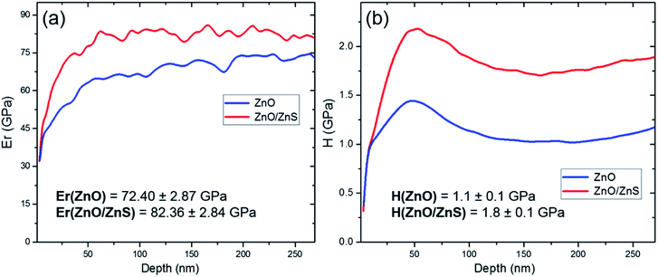 | ||
| Fig. 5 The evaluation of (a) Young's modulus and (b) hardness according to sample depth of ZnO and ZnO/ZnS nanofilms. | ||
Our results indicate that the addition of the thin ZnS top layer significantly improved the mechanical properties of the ZnO film and makes it more resistant to deformation. The thin ZnS layer enhances ZnO hardness and elastic modulus due to improving quality of ZnO surface.38,39 The passivation process of ZnO remove surface defects and significantly improved its mechanical properties, for example, elastic moduli in case of ZnO nanowires.38 The previous optical studies of the ZnO/ZnS nanofilms showed that sulfidation process removed ZnO surface defects.24 The cathodoluminescence (CL) intensity of the band-to-band emission for ZnO/ZnS nanolayer was one order of magnitude higher than that of ZnO. The emission mechanisms for ZnO nanolayers were enhanced, and their surface defects effectively passivated, by the ZnS film.40 The surface defects, sources of non-radiative recombination were removed by the ZnS coating formation. The crystal size is also a key factor influence mechanical properties. The hardness of ZnS nanobelts increased by 79% in comparison to bulk material and the nanostructures exhibited significant creep under a constant load indentation at room temperature.41 In our system, ZnS top layer consists of crystals with a diameter of 3 nm and enhances the hardness of ZnO film by 64%.
To confirm the higher mechanical stability of the film after ZnS coating, a nanowear test was performed by holding two different constant forces of 25 and 50 μN. The value of displaced material, calculated by the residual imprint, was estimated to be about 1.633 and 2.033 μm3 for 25 and 50 μN of applied force for ZnO films, respectively (Fig. 6). These values changed to 1.477 and 1.960 μm3 after the sulfidation process for films treated with 25 and 50 μN forces, respectively. Lower dislocate and damage material values were noted for ZnO/ZnS film at both applied forces, which suggests that the results are consistent with our nanomechanical tests.
The addition of a ZnS coating also influences the electrical properties of the ZnO nanofilms, which were investigated before and after the sulfidation process (Table 2). The conductivity of the ZnO film increases about 500-fold after ZnS coating. The ZnO/ZnS nanofilms are significantly more conductive because the passivation process removes surface defects and environmental influences. The thin ZnS layer releases oxygen molecules (O2) from ZnO surface, which can trap free carriers from the nanostructures. As a result of O2 and free-electron complex formation, the carrier density decreases at the surface of n-type ZnO, which is accompanied by greater depletion region. After passivation, ZnO is unable to react with gases, the trapped electrons are released and the conductivity increases. The mechanism has been described in detail for various 1D ZnO nanostructures such as nanowires42 and nanofibers,43 and for 2D structures such as nanowalls.44 The process has been proposed for use in various gas detectors, the sensitivity and selectivity of which depend on the ability for O2 to be removed from the semiconductor surface.
| ZnO film | ZnO/ZnS film | |
|---|---|---|
| Conductivity σ (1/Ω m) at 21 °C | 0.0039 | 1.8573 |
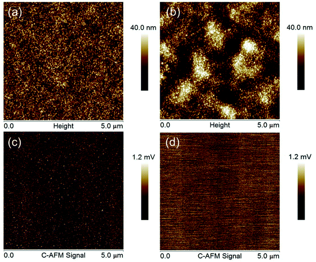
Fig. 7 shows the maps of electrical signal of ZnO and ZnO/ZnS nanofilms obtained by the C-AFM technique. The topography of the selected layer parts for C-AFM measurements was visualized by AFM in contact mode. The images were obtained for a large area of 5 μm × 5 μm to check the continuity of the electrical signal and breakdown presence. C-AFM maps for both films are characterized by a uniform signal and the layers do not have any region with higher or lower conductivity. Moreover, C-AFM maps do not contain the grain boundaries clearly visible on the layer topography images. The same result has been obtained for different scanning areas and samples. The voltage output of ZnO and ZnO/ZnS nanolayers is uniformly distributed across the whole surface, despite the polycrystalline nature of the films.
To study the stability of the samples in liquids, ZnO and ZnO/ZnS nanofilms were immersed in DI water. The experiment was carried out under ambient conditions and the nanofilms were not treated with any additional factors. After seven days, the ZnO nanolayer dissolved, while the ZnO/ZnS nanolayer remained stable and water-insoluble (Fig. 8). Residues of the crystals remained in some regions of the ZnO samples, which were not completely dissolved (Fig. 8(b)). ZnO-based materials are low stable in water, especially nanostructures due to their high surface area to volume ratio and a large number of surface defects in comparison to the bulk structures.45 The dissolution rate of ZnO nanomaterials in water depends on crystal size. The smaller ZnO grains dissolve in water much more quickly: ZnO nanofibers calcined at 700 °C remain water-stable much longer than nanofibers obtained at 500 °C due to the fact that crystal size was larger for nanostructures heated at a higher temperature.46 The mean diameter of ZnO crystals calcined at 500 °C was calculated previously based on SEM micrographs and it was estimated to be about 37 nm, but the size of some particles in the sample reached 60 nm.24 Most probably, either the experiment was too short for the dissolution of large crystals, or was sufficient to break the continuity of the layer but the liquid was not able to penetrate the closely-connected ZnO beads. ZnO nanostructures are usually dissolved in the hydrophilic fluids for a few hours and degraded into different ions, such as Zn2+, ZnO22− and Zn(NH3)42+ depending on the etching agent.47 The dissolution process is caused mainly due to ZnO surface polarity.48 ZnO nanocrystals are characterized by two sublattices consisting of corner-sharing tetrahedra with Zn2+ and O2− ions. It results in forming two faces, positively charged with zinc ions (0001) and negatively charged with oxygen ions (000-1). That arrangement allows interacting ZnO with both positive and negative charges.45 ZnS significantly decreases a surface charge and for example partially sulfidized ZnO nanoparticles decrease the rate of the dissolution process.49 In our system, ZnS thin layer completely covers ZnO surface and inhibits interaction with ions from the solution. It results in insolubility ZnO/ZnS films in a hydrophilic environment.
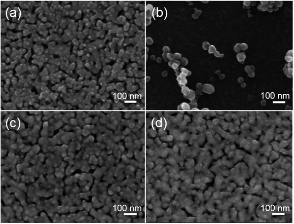 | ||
| Fig. 8 SEM images of (a and b) ZnO and (c and d) ZnO/ZnS nanofilms (a and c) untreated with water and (b and d) immersed in DI water for seven days. | ||
Our findings indicate that ZnS surface passivation in a gas phase of hydrogen sulfide is an effective way of protecting ZnO nanostructures against dissolution in a water-based environment. The protection of ZnO surfaces against environmental conditions, oxygen chemisorption and natural growth of ZnCO3 nanostructures is a crucial issue for the design of effective devices.50,51 ZnS is a common choice as a semiconductor for coating ZnO cores due to its high chemical stability at different pH values and its low toxicity.12 Additionally, the passivation process carried out in a gas phase allowed the polycrystalline structure of the base ZnO layer to be preserved, which did not change significantly. The active area, characterized by a high surface area to volume ratio, did not decrease after covering with ZnS. ZnO/ZnS nanofilms can be applied for different devices requiring a high surface area, such as sensors and biosensors, and the need to operate in different environments.
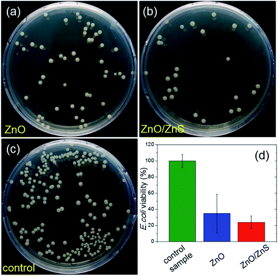
The antimicrobial properties of ZnO and ZnO/ZnS nanofilms were investigated against Gram-negative bacteria of E. coli. Fig. 9(a–c) shows the agar plates with bacterial colonies recultivated after deposition on ZnO and ZnO/ZnS nanolayers, and on a pure substrate as a control sample. Both nanolayer samples presented significantly fewer colonies, demonstrating their antimicrobial potential. A quantitative analysis of the bacterial survival rates was obtained by the colony forming unit count method. Fig. 9(d) presents the values of E. coli viability as below 40% and 30% for ZnO and ZnO/ZnS nanofilms, respectively, indicating that the ZnS coating does not have a negative influence on ZnO antibacterial properties and even slightly enhances them.
The antibacterial properties of ZnO are well known and are commonly applied for a range of treatments. ZnO materials enable the production of reactive oxygen species (ROS) such as peroxide (O2−2), hydroxyl radicals (OH−) and hydrogen peroxide (H2O2), which can inhibit bacterial growth.52 The other mechanism concerns the release and adhesion of Zn2+ ions from ZnO structures, resulting in mechanical damage to the cell wall.53 Additionally, the antimicrobial activity of ZnO may well be enhanced for nano-size materials due to their high surface area to volume ratio. In case of our films, their polycrystalline nature can also increase the ZnO-specific area and improve the antimicrobial reactivity.
The viability of the E. coli cells was found to slightly decrease after the sulfidation process, (Fig. 9(d)), which may be associated with the size of the ZnS crystals. In our previous study, the mean diameter of the crystal was estimated to be about 3 nm.24 The small size of the ZnS beads and the electrostatic interaction between the positively-charged ZnS crystals and the negatively-charged cell membrane resulted in easier interaction with bacteria and thus enhanced antibacterial effects against E. coli.54 Moreover, the ZnS surface layer can interact with thiol groups of the bacterial cell membrane protein and deactivate them, resulting in decreased permeability and leading to cell death.55
Conclusion
The study demonstrates that mechanical and electrical properties of ZnO polycrystalline nanofilms are enhanced after ZnS surface passivation. A coating of a ZnS thin layer was synthesized in a gas-phase sulfidation process, resulting in ZnO/ZnS film formation. The presence of ZnS was confirmed by infrared and Raman spectroscopy analysis. XRD patterns indicate that the ZnO parts have a wurtzite structure and suggest the creation of nanocrystalline ZnS. The Young's modulus and nanohardness were found to be about 14% and 64% greater following ZnS layer formation, and indicate lower susceptibility to damage. Nanowear tests carried out using nanoindentation methods and different applied forces found the dislocation and damage of materials to be lower with the ZnS-coated layer. Furthermore, the electrical conductivity of the ZnO nanofilms increased about 500-fold after ZnS formation as a result of surface defect passivation and the removal of oxygen molecules, which become incapable of reacting with free carriers. C-AFM maps found the top layer to be of high quality and free of defects, and the surface active area does not change significantly due to the fact that it forms in the presence of hydrogen sulphide and follows the morphology of the ZnO bottom film. The ZnS coating also enhances the stability of ZnO films in a biological environment. The ZnO/ZnS films were found to be insoluble in water for over seven days, while ZnO nanolayers dissolve. Additionally, ZnO antimicrobial properties against E. coli slightly increased after ZnS passivation. Our findings indicate that ZnO surface passivation is required for designing future devices to improve its stability in different environments and to enhance its mechanical, electrical and antibacterial properties.Conflicts of interest
There are no conflicts to declare.Acknowledgements
The research was supported by Polish Ministry of Science and Higher Education (Grant “Iuventus Plus” No. 0018/IP2/2015/73, 2015-2017) and Nation Centre for Research and Development (PBS1/A9/13/2012). The authors thank Dr Zuzanna Pietralik (Department of Macromolecular Physics, Adam Mickiewicz University) for assistance during FTIR measurements.References
- M. Singh, K. Manoli, A. Tiwari, T. Ligonzo, C. Di Franco, N. Cioffi, G. Palazzo, G. Scamarcio and L. Torsi, J. Mater. Chem. C, 2017, 5, 3509–3518 RSC.
- H. Singh, A. Kumar, B. S. Bansod, T. Singh, A. Thakur, T. Singh and J. Sharma, RSC Adv., 2018, 8, 3839–3845 RSC.
- Y. C. Chang, J. Alloys Compd., 2016, 664, 538–546 CrossRef.
- Y.-C. Liang and C.-C. Wang, RSC Adv., 2018, 8, 5063–5070 RSC.
- A. Sadollahkhani, I. Kazeminezhad, J. Lu, O. Nur, L. Hultman and M. Willander, RSC Adv., 2014, 4, 36940–36950 RSC.
- D. Chen, F. Huang, G. Ren, D. Li, M. Zheng, Y. Wang and Z. Lin, Nanoscale, 2010, 2, 2062–2064 RSC.
- W. Tian, C. Zhang, T. Zhai, S. L. Li, X. Wang, J. Liu, X. Jie, D. Liu, M. Liao, Y. Koide, D. Golberg and Y. Bando, Adv. Mater., 2014, 26, 3088–3093 CrossRef PubMed.
- X. Gu, S. Zhang, Y. Zhao and Y. Qiang, Vacuum, 2015, 122, 6–11 CrossRef.
- E. M. Flores, C. W. Raubach, R. Gouvea, E. Longo, S. Cava and M. L. Moreira, Mater. Chem. Phys., 2016, 173, 347–354 CrossRef.
- G. Cao, H. Yang, K. Hong, W. Hu and M. Xu, Mater. Lett., 2015, 161, 278–281 CrossRef.
- A. Brayek, S. Chaguetmi, M. Ghoul, I. Ben Assaker, A. Souissi, L. Mouton, P. Beaunier, S. Nowak, F. Mammeri, R. Chtourou and S. Ammar, RSC Adv., 2016, 6, 30919–30927 RSC.
- A. Baranowska-Korczyc, K. Sobczak, P. Dłuzewski, A. Reszka, B. J. Kowalski, Ł. Kłopotowski, D. Elbaum and K. Fronc, Phys. Chem. Chem. Phys., 2015, 17, 24029–24037 RSC.
- R. Zhang, B. Wang, H. Zhang and L. Wei, Appl. Surf. Sci., 2005, 241, 435–441 CrossRef.
- S. Tarish, Z. Wang, A. Al-Haddad, C. Wang, A. Ispas, H. Romanus, P. Schaaf and Y. Lei, J. Phys. Chem. C, 2015, 119, 1575–1582 CrossRef.
- H. Zhao, Y. Dong, P. Jiang, X. Wu, R. Wu and Y. Chen, RSC Adv., 2015, 5, 6494–6500 RSC.
- D. Bao, P. Gao, X. Zhu, S. Sun, Y. Wang, X. Li, Y. Chen, H. Zhou, Y. Wang and P. Yang, Chem.–Eur. J., 2015, 21, 12728–12734 CrossRef PubMed.
- S. Zhang, B. Yin, H. Jiang, F. Qu, A. Umar and X. Wu, Dalton Trans., 2014, 44, 2409–2415 RSC.
- S. C. Rai, K. Wang, Y. Ding, J. K. Marmon, M. Bhatt, Y. Zhang, W. Zhou and Z. L. Wang, ACS Nano, 2015, 9, 6419–6427 CrossRef PubMed.
- Z. Zhao, C. Jiang, X. Pu, C. Du, L. Li, B. Ma and W. Hu, Appl. Phys. Lett., 2016, 108, 153104 CrossRef.
- B. Ji, J. Zhang, C. Zhang, N. Li, T. Zhao, F. Chen, L. Hu, S. Zhang and Z. Wang, ACS Appl. Nano Mater., 2018, 1, 793–799 CrossRef.
- A. K. Giri, C. Charan, A. Saha, V. K. Shahi and A. B. Panda, J. Mater. Chem. A, 2014, 2, 16997–17004 RSC.
- A. Baranowska-Korczyc, K. Fronc and D. Elbaum, Method for preparing metal oxide layers, Polish Patent Office, Patent No. PL401419-A1, PL220304-B1, 2014.
- A. Baranowska-Korczyc, K. Fronc and D. Elbaum, Passivation method of ZnO nanostructures, Polish Patent Office, Patent No. PL220716-B1, 2014.
- A. Baranowska-Korczyc, A. Reszka, K. Sobczak, T. Wojciechowski and K. Fronc, J. Alloys Compd., 2017, 695, 1196–1204 CrossRef.
- W. C. Oliver and D. M. Pharr, J. Mater. Res., 1992, 7, 1564–1583 CrossRef.
- J. Fu, J. Ji, W. Yuan and J. Shen, Biomaterials, 2005, 26, 6684–6692 CrossRef PubMed.
- S. Karamdoust, B. Yu, C. V. Bonduelle, Y. Liu, G. Davidson, G. Stojcevic, J. Yang, W. M. Lau and E. R. Gillies, J. Mater. Chem., 2012, 22, 4881 RSC.
- S. S. Kawar and B. H. Pawar, J. Mater. Sci.: Mater. Electron., 2010, 21, 906–909 CrossRef.
- A. K. Thottoli, A. Kaliani and A. Unni, J. Nanostruct. Chem., 2013, 3, 1 Search PubMed.
- R. Zamiri, D. M. Tobaldi, H. A. Ahangar, A. Rebelo, M. P. Seabra, M. S. Belsley and J. M. F. Ferreira, RSC Adv., 2014, 4, 35383–35389 RSC.
- G. Socrates, Infrared and Raman characteristic group frequencies: Tables and Charts, Wiley, New York, 3rd edn, 2001 Search PubMed.
- Ü. Özgür, Y. I. Alivov, C. Liu, A. Teke, M. A. Reshchikov, S. Doǧan, V. Avrutin, S. J. Cho and H. Mork
![[o with combining cedilla]](https://www.rsc.org/images/entities/char_006f_0327.gif) , J. Appl. Phys., 2005, 98, 1–103 CrossRef.
, J. Appl. Phys., 2005, 98, 1–103 CrossRef. - T. L. Phan, R. Vincent, D. Cherns, N. X. Nghia and V. V Ursaki, Nanotechnology, 2008, 19, 475702 CrossRef PubMed.
- Y. C. Cheng, C. Q. Jin, F. Gao, X. L. Wu, W. Zhong, S. H. Li and P. K. Chu, J. Appl. Phys., 2009, 106, 123505 CrossRef.
- A. G. Milekhin, N. A. Yeryukov, L. L. Sveshnikova, T. A. Duda, C. Himcinschi, E. I. Zenkevich and D. R. T. Zahn, Appl. Phys. A: Mater. Sci. Process., 2012, 107, 275–278 CrossRef.
- T. Fang, W. Chang and C. Lin, Mater. Sci. Eng., A, 2007, 452, 715–720 CrossRef.
- S. R. Jian, J. S. C. Jang, G. J. Chen, H. G. Chen and Y. T. Chen, J. Alloys Compd., 2009, 479, 348–351 CrossRef.
- A. Roy, J. Mead, S. Wang and H. Huang, Sci. Rep., 2017, 7, 1–8 CrossRef PubMed.
- S. S. Bhat, U. V. Waghmare and U. Ramamurty, Comput. Mater. Sci., 2015, 99, 133–137 CrossRef.
- L. Liu, Y. Chen, T. Guo, Y. Zhu, Y. Su, C. Jia, M. Wei and Y. Cheng, ACS Appl. Mater. Interfaces, 2012, 4, 17–23 CrossRef PubMed.
- X. Li, X. Wang, Q. Xiong and P. C. Eklund, Nano Lett., 2005, 5, 1982–1986 CrossRef PubMed.
- D. Zhang, S. Chava, C. Berven, S. K. Lee, R. Devitt and V. Katkanant, Appl. Phys. A, 2010, 100, 145–150 CrossRef.
- A. Baranowska-Korczyc, K. Fronc, Ł. Kłopotowski, A. Reszka, K. Sobczak, W. Paszkowicz, K. Dybko, P. Dłuzewski, B. J. Kowalski and D. Elbaum, RSC Adv., 2013, 3, 5656–5662 RSC.
- T. P. Chen, S. P. Chang, F. Y. Hung, S. J. Chang, Z. S. Hu and K. J. Chen, Sensors, 2013, 13, 3941–3950 CrossRef PubMed.
- J. Hupkes, J. I. Owen, S. E. Pust and E. Bunte, ChemPhysChem, 2012, 13, 66–73 CrossRef PubMed.
- A. Stafiniak, B. Boratyński, A. Baranowska-Korczyc, K. Fronc, D. Elbaum, R. Paszkiewicz and M. Tłaczała, J. Mater. Sci., 2013, 31, 312–317 Search PubMed.
- J. Zhou, N. Xu and Z. L. Wang, Adv. Mater., 2006, 18, 2432–2435 CrossRef.
- A. Stafiniak, B. Boratyński, A. Baranowska-Korczyc, W. Mecherzyński, K. Fronc, R. Paszkiewicz, M. Tłaczała and D. Elbaum, J. Mater. Sci. Eng. B, 2012, 177, 1299–1303 CrossRef.
- R. Ma, C. Levard, F. M. Michel, G. E. Brown and G. V Lowry, Environ. Sci. Technol., 2013, 47, 2527–2534 CrossRef PubMed.
- Z. Pan, J. Tao, Y. Zhu, J. F. Huang and M. Parans Paranthaman, Chem. Mater., 2010, 22, 149–154 CrossRef.
- T.-H. Huang, P.-K. Yang, D.-H. Lien, C.-F. Kang, M.-L. Tsai, Y.-L. Chueh and J.-H. He, Sci. Rep., 2014, 4, 4402 CrossRef PubMed.
- A. Sirelkhatim, S. Mahmud, A. Seeni, N. H. M. Kaus, L. C. Ann, S. K. M. Bakhori, H. Hasan and D. Mohamad, Nano-Micro Lett., 2015, 7, 219–242 CrossRef.
- V. B. S. Mallakpour, Eur. Polym. J., 2016, 84, 377–403 CrossRef.
- G. Li, J. Zhai, D. Li, X. Fang, H. Jiang, Q. Dong and E. Wang, J. Mater. Chem., 2010, 20, 9215–9219 RSC.
- V. K. Gupta, D. Pathania, M. Asif and G. Sharma, J. Mol. Liq., 2014, 196, 107–112 CrossRef.
| This journal is © The Royal Society of Chemistry 2018 |

