 Open Access Article
D–A–D 2H-benzo[d][1,2,3]triazole derivatives as p-type semiconductors in organic field-effect transistors†
Iván Torres-Moya*a,
Iratxe Arrechea-Marcosb,
Carlos Tardíoa,
José R. Carrillo a,
Ángel Díaz-Ortiz
 a,
J. Teodomiro López Navarreteb,
M. Carmen Ruiz Delgado
 b,
Pilar Prieto
 *a and
Rocío Ponce Ortiz
 *b
*b
aDepartment of Organic Chemistry, Faculty of Chemical and Technologies Sciences, University of Castilla La Mancha-IRICA, 13071 Ciudad Real, Spain. E-mail: MariaPilar.Prieto@uclm.es; Ivan.TorresMoya@uclm.es
bDepartment of Physical Chemistry, Faculty of Sciences, University of Málaga, 29071 Málaga, Spain. E-mail: rocioponce@uma.es
First published on 13th June 2018
Abstract
A series of Donor–π–Acceptor–π–Donor compounds based on a 2H-benzo[d][1,2,3]triazole core branched with different alkynyl donor groups has been characterized and tested in organic field-effect transistors (OFETs). The electronic and molecular structures were elucidated through optical and vibrational spectroscopy in conjunction with DFT calculations. The results indicate that the planarity of the structure and the good intramolecular charge transfer from the electron-donating to the electron-withdrawing fragments play a critical role in the application of the compounds as semiconductors in OFET devices. The compounds were tested in a top-contact/bottom-gate thin film transistor architecture, and they behave as p-type semiconductors.
Introduction
Organic multifunctional semiconducting derivatives have attracted a great deal of attention in the last decade due to their potential applications in organic electronics, such as organic field-effect transistors (OFETs), organic solar cells, sensors, photodetectors and optical waveguide devices.1 These compounds have advantages that include low-cost, flexibility and bio-compatibility.2There is a plethora of organic molecules that have been used as organic semiconductors, including polymers and oligomers with donor–acceptor (D–A) architectures, that consist of an electron donor (D) and an electron acceptor (A) connected by a π-conjugated bridge, which facilitates intramolecular charge transfer (ICT).3 In these compounds, modifying their electronic structures with the aim of developing low-band gap semiconductors with high charge-carrier mobilities is feasible. Variation of the HOMO and LUMO energy values through the introduction of different donor and acceptor groups is the best strategy to tune the electronic and optoelectronic properties of these systems for device applications. Given the variety of chemical synthesis methods, the organic semiconducting materials can be modified to fulfill the demands of different applications.4
However, the performance of organic semiconductors is governed not only by the molecular structure but also by how molecules or polymer chains assemble in the solid state.5 Intermolecular interactions such as hydrogen bonding, π–π stacking and electrostatic forces can be used to tune the factors that influence the self-assembly and the final morphologies of the aggregates. Compared with thin films, one-dimensional (1D) organic semiconductors, due to their confined sizes and unique shapes, have proven to exhibit novel properties.6,7 Furthermore, the more ordered packing structures in 1D crystalline organic semiconductors lead to relatively better and more reproducible device performance.8 On the other hand, 1D organic semiconductors have fewer grain boundaries and defects and this gives rise to better charge-carrier transport properties. An understanding of structure-property relationships is therefore an important goal.
Among all the electronic devices, organic field effect transistors (OFETs) have attracted enormous interest.9 These devices consist of an organic semiconducting layer, a gate insulator layer, and three terminals (source, drain and gate electrodes). OFETs are essential building blocks for the next generation of cheap and flexible organic circuits. However, they also provide an important insight into the charge transport of π-conjugated systems.10 Therefore, OFETs have been the focus of attention for numerous researchers in the last two decades because of their enormous potential as fundamental elements in electronic devices, such as electronic papers,11 displays,12 radio frequency identification (RFID) tags, and sensors.13
In addition to this, multifunctionality is greatly desirable in materials science. In this sense, the appropriate choice of substituents allows control not only of the structure of the material but also of its properties. Thus, appropriate control of the starting molecular components enables the formation of supramolecular nanoscopic architectures that combine several properties and have a range of potential applications.14,15
In this respect, the 2H-benzo[d][1,2,3]triazole ring is an electron-deficient system that plays an important role as an acceptor moiety. This unit can be easily modified by alkylation at the central nitrogen and the introduction of different groups in the benzene ring, thus making it an excellent unit with great applicability in different fields.16
Some of us previously described the self-assembly of 2H-benzo[d][1,2,3]triazole derivatives to afford ribbons exhibiting an optical waveguiding behavior.17,18 In an effort to highlight the multifunctionality of these compounds, in this paper we describe the characterization and application as organic field-effect transistors of ten 2H-benzo[d][1,2,3]triazole derivatives. The electronic and molecular structures of these organic semiconductors were analyzed by DFT calculations, Raman spectroscopy, AFM techniques, and XRD, amongst others. The electrical performance of the materials was tested in OFET devices and they showed potential as p-type semiconductors.
Results and discussion
In this work, the applicability of 2H-benzo[d][1,2,3]triazole (Bzt-Ar) derivatives (Scheme 1) as p-type semiconductors in OFETs has been evaluated in order to assess their multifunctionality. It is well known that molecules with highly planar backbones and widely delocalized π-conjugation usually show efficient supramolecular order, good charge mobility and therefore are promising candidates as semiconductor materials in organic electronics. In this sense, benzotriazole derivatives appear to be excellent moieties to achieve this goal, when functionalized with electron rich groups19 with different electronic effects as described here.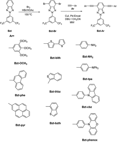 | ||
| Scheme 1 Synthesis of 2-(3,5-bis(trifluoromethyl)phenyl)-4,7-bis(arylethynyl)-2H-benzo[d][1,2,3]triazole derivatives (Bzt-Ar) by a Sonogashira cross-coupling reaction between Bzt-Br and Ar. | ||
As a first approach, with the aim of determining the possible applicability of these compounds as semiconductor layers in OFETs, different aspects related to molecular geometry and electronic properties have been studied theoretically and experimentally. Computational calculations constitute a powerful tool in order to elucidate the experimental data and to assess information on the mechanism of charge transport in organic materials. Furthermore, theoretical calculations can be used to predict molecular properties, thus supporting a rational design of new materials, avoiding unnecessary synthesis. In this work, theoretical DFT calculations of the studied organic semiconductors have been carried out at the B3LYP/6-31G(d,p) level in order to establish structure-property relationships.
(a) DFT-optimized geometries
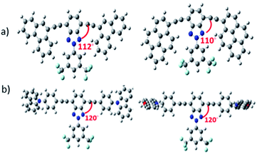
DFT theoretical calculations on the 2-(3,5-bis(trifluoromethyl)phenyl)-2H-benzo[d][1,2,3]triazole derivatives indicate that the benzotriazole core and the arylalkynyl fragment are basically coplanar (Table S1†), which is desirable for achieving effective π-conjugation. However, the functionalization with different alkyl groups can have an impact on skeleton planarity. In fact, a certain torsion angle between the benzotriazole core and the donor group is found for some of the studied semiconductors. For example, in Bzt-phe and Bzt-pyr the dihedral angle is close to 110° (Fig. 1a) due to steric hindrance between the hydrogen atoms of the phenanthrene (Bzt-phe) or pyrene (Bzt-pyr) units and the trifluoromethyl groups.It is worth mentioning that in Bzt-cbz and Bzt-phenox the donor fragment is perpendicular to the central core, which could have a detrimental effect on their crystal packing and therefore on their electrical properties (Fig. 1b).
(b) DFT-calculated molecular orbital energies and topologies and photophysical data
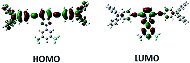
DFT calculations indicate similar frontier molecular orbital topologies for all derivatives. As an example, the topologies of the HOMO and LUMO orbitals of Bzt-tpa are depicted in Fig. 2. The HOMO orbital is located on the arylalkynyl fragment and the LUMO orbital in the benzotriazole core. Moreover there is an overlap between HOMO and LUMO orbitals, which indicates the intramolecular charge transfer character of the HOMO–LUMO transition.Experimental optical absorption and photoluminescence spectra were recorded in order to determine the ICT character of the HOMO–LUMO transition and to quantify band gap energy values.
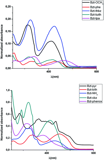
These spectra were recorded for diluted solutions of compounds Bzt-Ar in chloroform (Fig. 3, Fig. S1† and Table 1). It can be observed from the absorption spectra that all of these compounds show two bands, being the lowest energy one characteristic of intramolecular charge transfer (ICT),20 and ascribed theoretically to a HOMO–LUMO transition. In addition, on the basis of these results, the optical band gaps were estimated from the onset of the lowest energy absorptions and were found to be in good agreement with the theoretical calculations (Table 1).
| Compound | λmax (nm) | ε (M−1 cm−1) | λonset (nm) | Egap (eV) |
|---|---|---|---|---|
| Bzt-OCH3 | 412 | 11![[thin space (1/6-em)]](https://www.rsc.org/images/entities/char_2009.gif) 00 00![[thin space (1/6-em)]](https://www.rsc.org/images/entities/char_2009.gif) 000 000 |
481 | 2.58 (2.81) |
| Bzt-phe | 421 | 3![[thin space (1/6-em)]](https://www.rsc.org/images/entities/char_2009.gif) 00 00![[thin space (1/6-em)]](https://www.rsc.org/images/entities/char_2009.gif) 000 000 |
498 | 2.49 (2.64) |
| Bzt-pyr | 439 | 17![[thin space (1/6-em)]](https://www.rsc.org/images/entities/char_2009.gif) 00 00![[thin space (1/6-em)]](https://www.rsc.org/images/entities/char_2009.gif) 000 000 |
540 | 2.30 (2.39) |
| Bzt-bith | 455 | 8![[thin space (1/6-em)]](https://www.rsc.org/images/entities/char_2009.gif) 00 00![[thin space (1/6-em)]](https://www.rsc.org/images/entities/char_2009.gif) 000 000 |
536 | 2.31 (2.39) |
| Bzt-thbz | 424 | 17![[thin space (1/6-em)]](https://www.rsc.org/images/entities/char_2009.gif) 00 00![[thin space (1/6-em)]](https://www.rsc.org/images/entities/char_2009.gif) 000 000 |
495 | 2.50 (2.27) |
| Bzt-bzth | 411 | 4![[thin space (1/6-em)]](https://www.rsc.org/images/entities/char_2009.gif) 00 00![[thin space (1/6-em)]](https://www.rsc.org/images/entities/char_2009.gif) 000 000 |
476 | 2.60 (2.77) |
| Bzt-NH2 | 434 | 6![[thin space (1/6-em)]](https://www.rsc.org/images/entities/char_2009.gif) 00 00![[thin space (1/6-em)]](https://www.rsc.org/images/entities/char_2009.gif) 000 000 |
506 | 2.45 (2.48) |
| Bzt-tpa | 464 | 3![[thin space (1/6-em)]](https://www.rsc.org/images/entities/char_2009.gif) 20 20![[thin space (1/6-em)]](https://www.rsc.org/images/entities/char_2009.gif) 000 000 |
556 | 2.29 (2.39) |
| Bzt-cbz | 414 | 45![[thin space (1/6-em)]](https://www.rsc.org/images/entities/char_2009.gif) 00 00![[thin space (1/6-em)]](https://www.rsc.org/images/entities/char_2009.gif) 000 000 |
480 | 2.58 (2.58) |
| Bzt-phenox | 384 | 45![[thin space (1/6-em)]](https://www.rsc.org/images/entities/char_2009.gif) 00 00![[thin space (1/6-em)]](https://www.rsc.org/images/entities/char_2009.gif) 000 000 |
581 | 2.13 (1.89) |
Moreover, the determination of HOMO and LUMO energy levels is feasible by cyclic voltammetry measurements. In this case these measures were performed on 1.5 × 10⁻⁴ M chloroform solutions of the compounds using 0.1 M tetrabutylammoniumhexafluorophosphate (NBu4PF6) as the supporting electrolyte (Table 2, Fig. 4 and S2–S10 in the ESI†). An Ag/AgCl electrode was used as the reference and potentials were referenced against the ferrocene/ferrocenium redox couple (0.1 V vs. SCE). From these data, the ionization potential (EHOMO) and electron affinity (ELUMO) values were estimated for the novel semiconductors. These values were calculated from the oxidation and reduction potential data by using standard approximations [eqn (1) and (2)], considering that the energy level of ferrocene/ferrocenium is 4.80 eV lower in vacuum.21 The values obtained are listed in Table 2.
| EHOMO = −(Eox + 4.80) (eV) | (1) |
| ELUMO = −(Ered + 4.80) (eV) | (2) |
| Entry | Compound | Ereda | Eoxa | HOMOb (eV) | LUMOb (eV) |
|---|---|---|---|---|---|
| a Electrochemical potentials vs. saturated calomel electrode (SCE) for compounds Bzt-Ar in CHCl3.b Frontier orbital energies calculated from cyclic voltammetry data. | |||||
| 1 | Bzt-OCH3 | −1.52 | 1.64 | −6.07 | −2.91 |
| 2 | Bzt-phe | −1.56 | 1.61 | −6.04 | −2.87 |
| 3 | Bzt-pyr | −1.48 | 1.59 | −6.02 | −2.95 |
| 4 | Bzt-bith | −1.50 | 1.35 | −5.78 | −2.93 |
| 5 | Bzt-thbz | −1.63 | 1.08 | −5.51 | −2.80 |
| 6 | Bzt-bzth | −1.70 | 1.68 | −6.11 | −2.73 |
| 7 | Bzt-NH2 | −1.52 | 0.99 | −5.42 | −2.91 |
| 8 | Bzt-tpa | −1.26 | 1.30 | −5.73 | −3.17 |
| 9 | Bzt-cbz | −1.36 | 1.50 | −5.93 | −3.07 |
| 10 | Bzt-phenox | −1.69 | 0.98 | −6.11 | −2.74 |
It is worth noting that the Ered values are similar for all compounds indicating comparable LUMO energy levels. As indicated by the theoretical calculations, the LUMO is located on the benzotriazole core, which is common to all of the semiconductors, and thus the similar values. The major differences appear in the Eox related to HOMO values, which is logic considering that HOMO orbitals are located on the donor groups, and those vary from molecule to molecule.
Therefore, the introduction of different substituents in the alkynyl fragment allows modulation of the semiconductor donor ability. By comparing donor groups containing a nitrogen atom it becomes clear that compounds where an electron pair is available (i.e. Bzt-NH2, Bzt-tpa and Bzt-phenox) show enhanced donor ability (Table 2, entries 7, 8 and 10). In contrast, compound Bzt-cbz, which does not have an available lone pair on the nitrogen because it takes part in the aromatic system, has the highest oxidation potential. In this sense, the results show superior donor ability of the nitrogen derivative (Bzt-NH2) when compared to the oxygen derivative (Bzt-OCH3) (Table 2, entries 7 and 1).
It should be pointed out that the redox processes are difficult in compounds with a thiophene moiety, such as Bzt-bith and Bzt-bzth (Table 2, entries 4 and 6). A plausible explanation is that delocalization of the charges into the electrogenerated radicals, which disrupts the aromaticity of the thiophene ring, requires a higher electron cost.
In all compounds, the HOMO values are close to the Fermi level of Au, indicating a potential flow of positive charge carriers between the HOMO orbital and the metal. For these reason, it could be expected that these BTz derivatives could behave as a p-type semiconductors.
(c) DFT-caculated intramolecular reorganization energies
One fundamental theoretical parameter that can be related to charge transport is the intramolecular reorganization energy, which reflects the geometric changes needed to accommodate charge. Thus, lower reorganization energies normally are associated with more efficient charge transport. This parameter has been calculated as reported previously.22 In particular, the intramolecular reorganization energy (λ) associated with an intermolecular charge transfer reaction consists of two terms related to the geometry relaxation energies upon going from the neutral state to a charged molecular state and vice versa, and it is given by the expression (eqn (3)):| λ = λrel(1) + λrel(2) | (3) |
| λrel(1) = E(1)(N) − E(0)(N) | (4) |
| λrel(2) = E(1)(I) − E(0)(I) | (5) |
Following this procedure, λ calculated values at the B3LYP/6-31G(d,p) level for all compounds are shown in Table 3. As these compounds are expected to act as p-type semiconductors, the reorganization energies have only been calculated for hole transport.23
| Compound | λh (eV) |
|---|---|
| Bzt-OCH3 | 0.33 |
| Bzt-phe | 0.19 |
| Bzt-pyr | 0.14 |
| Bzt-bith | 0.16 |
| Bzt-thbz | 0.20 |
| Bzt-bzth | 0.18 |
| Bzt-NH2 | 0.38 |
| Bzt-tpa | 0.20 |
| Bzt-cbz | 0.14 |
| Bzt-phenox | 0.18 |
Moderate reorganization energies were predicted for all the compounds, with values in the range between 0.14 and 0.38 eV. These values are on the same order than other benchmark hole-transport materials, such as rubrene (0.16 eV)24 or phenyl-substituted dithienoacene (0.31 eV).25 Within the series, the compounds showing the highest values are Bzt-OCH3 and Bzt-NH2, which can be related with the greater conformational freedom of the lateral substituents. Therefore, our results show that the easy one-electron reversible oxidation of our Donor–π–Acceptor–π–Donor systems together with their moderate predicted values of hole intramolecular reorganization energy would render them as potential hole-transport material candidates.
(d) Raman spectroscopy
FT-Raman spectra were also recorded in order to gather information on the degree of π-conjugation of the various semiconductors, as previously demonstrated for other types of organic materials.26,27 More conjugated structures are desirable for efficient stabilization of the injected charge. Theoretical Raman spectra were obtained by DFT calculations and the results were compared with the experimental ones. The obtained results are collected in Table 4.| Compound | Benzotriazole band (cm−1) | C![[triple bond, length as m-dash]](https://www.rsc.org/images/entities/char_e002.gif) C triple bond stretching (cm−1) C triple bond stretching (cm−1) |
|---|---|---|
| Bzt-OCH3 | 1474 (1462) | 2202 (2300) |
| Bzt-phe | 1474 (1460) | 2197 (2287) |
| Bzt-pyr | 1476 (1460) | 2207 (2277) |
| Bzt-bith | 1473 (1459) | 2187 (2272) |
| Bzt-thbz | 1472 (1456) | 2193 (2259) |
| Bzt-bzth | 1472 (1461) | 2200 (2295) |
| Bzt-NH2 | 1473 (1461) | 2204 (2291) |
| Bzt-tpa | 1475 (1461) | 2198 (2289) |
| Bzt-cbz | 1474 (1461) | 2193 (2296) |
| Bzt-phenox | 1472 (1461) | 2210 (2300) |
We will focus our discussion on the analysis of two characteristic bands: the vibration recorded at ∼1470 cm−1 located on the benzotriazole group and the stretching vibration of the C![[triple bond, length as m-dash]](https://www.rsc.org/images/entities/char_e002.gif) C triple bond, at ∼2200 cm−1. No remarkable changes are recorded for the vibration at ∼1470 cm−1. In marked contrast, the ν(C
C triple bond, at ∼2200 cm−1. No remarkable changes are recorded for the vibration at ∼1470 cm−1. In marked contrast, the ν(C![[triple bond, length as m-dash]](https://www.rsc.org/images/entities/char_e002.gif) C) is highly sensitive to the donor group variation. For this reason, this latter band is optimal to evaluate the effectiveness of the different semiconductors. Thus, a downshift of this Raman vibration indicates more effective π–π conjugation and therefore, improved intramolecular charge transfer.
C) is highly sensitive to the donor group variation. For this reason, this latter band is optimal to evaluate the effectiveness of the different semiconductors. Thus, a downshift of this Raman vibration indicates more effective π–π conjugation and therefore, improved intramolecular charge transfer.
As an example, a comparison between the experimental and theoretical Raman spectra for Bzt-OCH3 is shown in Fig. 5. Other spectra can be found in the ESI (Fig. S11–S19†).
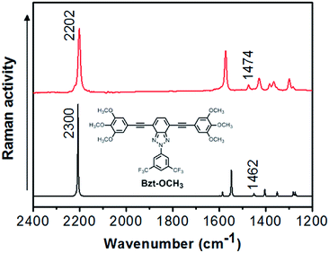 | ||
| Fig. 5 Comparison between experimental Raman spectra (red) and theoretical Raman spectra (black) for Bzt-OCH3. Theoretical spectra were calculated at the B3LYP/6-31G(d,p) theory level. | ||
Comparison of compounds with thiophene groups (Bzt-bith, Bzt-thbz and Bzt-bzth) shows displacements of the C![[triple bond, length as m-dash]](https://www.rsc.org/images/entities/char_e002.gif) C triple bond stretching due to the different degree of π-conjugation. In particular, the displacement of this vibration toward lower wavenumbers follows the trend: Bzt-bzth → Bzt-thbz → Bzt-bith, indicating that a thiophene ring linker between acceptor and donor groups is somewhat desirable for efficient π-conjugation. On the contrary, the more aromatic character of the benzene ring prevents efficient charge delocalization, diminishing intramolecular charge transfer.
C triple bond stretching due to the different degree of π-conjugation. In particular, the displacement of this vibration toward lower wavenumbers follows the trend: Bzt-bzth → Bzt-thbz → Bzt-bith, indicating that a thiophene ring linker between acceptor and donor groups is somewhat desirable for efficient π-conjugation. On the contrary, the more aromatic character of the benzene ring prevents efficient charge delocalization, diminishing intramolecular charge transfer.
In the cases of Bzt-phe and Bzt-pyr, where the donor group is a phenanthrene and a pyrene, respectively, it can be observed that the displacement is less marked in Bzt-phe than in Bzt-pyr. As a result, the π conjugation must be better in Bzt-phe despite the fact that the number of rings is lower than in Bzt-pyr. This situation is similar to the previous case. In Bzt-pyr, in contrast to the expected behaviour, the higher number of benzene rings improves the charge delocalization in the structure but makes the internal charge transfer between the donor and acceptor group more difficult, this effect increasing with the number of rings.
Finally, donor groups that contain nitrogen atoms, such as in Bzt-NH2, Bzt-tpa, Bzt-cbz and Bzt-phenox, were compared. The compounds Bzt-tpa, Bzt-cbz and Bzt-phenox contain a large number of benzene rings and, for this reason, aromatization must be higher than in Bzt-NH2, which contains only one aniline group. However, the ν(C![[triple bond, length as m-dash]](https://www.rsc.org/images/entities/char_e002.gif) C) vibration appears at higher wavenumber in Bzt-phenox than in Bzt-NH2. The phenylphenoxazine group is highly electron-withdrawing and therefore attracts the charge strongly, thus leading to worse delocalisation than in the other cases. On the other hand, the difference between Bzt-tpa and Bzt-cbz can be related to structural parameters. Note that while the triphenylamine group is not planar the phenylcarbazole is indeed planar, improving the π-conjugation and charge delocalisation which is supported by the downshift of the ν(C
C) vibration appears at higher wavenumber in Bzt-phenox than in Bzt-NH2. The phenylphenoxazine group is highly electron-withdrawing and therefore attracts the charge strongly, thus leading to worse delocalisation than in the other cases. On the other hand, the difference between Bzt-tpa and Bzt-cbz can be related to structural parameters. Note that while the triphenylamine group is not planar the phenylcarbazole is indeed planar, improving the π-conjugation and charge delocalisation which is supported by the downshift of the ν(C![[triple bond, length as m-dash]](https://www.rsc.org/images/entities/char_e002.gif) C) band.
C) band.
In general, there is a good agreement between theoretical and experimental results. Bearing in mind the Raman spectroscopy results, the HOMO energy levels, the reorganization energy values and the geometry calculated, it can be expected Bzt-phe, Bzt-bith, Bzt-bzth, Bzt-tpa and Btz-cbz to be the best candidates as semiconductors in OFETs. However, note that other supramolecular parameters, such as molecular ordering within the thin film are crucial in the charge transport process, and may control the device performance.
(e) Electrical characterization
The charge-transport properties of the benzotriazole derivatives and their behaviour as organic semiconductors were evaluated by fabricating top-contact/bottom-gate field-effect transistors by organic semiconductor vapour deposition in vacuum on Si/SiO2 substrates treated with octadecyltrichlorosilane (OTS) or hexamethyldisilazane (HMDS), followed by thermal gold deposition using shadow masks to define the source and drain electrodes. The parameters required to define the properties and behaviour as an OFET can be extracted from the I–V response plots in the saturation regime by using the assumptions of conventional transistor formalisms [eqn (6)]. The efficiency of OFETs can be determined by the drain current in the saturation regime ((ID)sat) [eqn (6)], where W is the channel width, L the channel length, C the capacitance per unit area or the insulator layer and VG the gate voltage. The calculated parameters are field-effect mobility (μ), ION/IOFF ratio and threshold voltage (VT).28,29| (ID)sat = (W/2L)μC(VG − VT)2 | (6) |
The OFET parameter data for films of Bzt-Ar are summarized in Table 5. It should be pointed out that these results correspond to HMDS-treated Si/SiO2 substrates as these provided better electrical figures. To calculate these parameters, transfer plots of (ID)sat vs. VG were used to determine the saturation mobility, ION/IOFF ratio and threshold voltage for the different fabricated devices. The parameters were calculated with VD = 100 V for hole transport. Some representative output and transfer plots for Bzt-tpa are shown in Fig. 6.
| Semiconductor (HMDS 90 °C) | μh (cm2 V−1 s−1) | VT (V) | ION/IOFF |
|---|---|---|---|
| Bzt-phe | 2.69 × 10⁻⁴ | −57 | 2 × 10³ |
| Bzt-pyr | 3.31 × 10⁻⁵ | −40 | 1 × 10² |
| Bzt-thbz | 1.80 × 10⁻⁴ | −69 | 8 × 10³ |
| Bzt-bzth | 3.76 × 10⁻⁵ | −13 | 4 × 10² |
| Bzt-tpa | 1.21 × 10⁻⁴ | −38 | 2 × 10² |
| Bzt-cbz | 2.02 × 10⁻⁵ | −58 | 3 × 10² |
| Bzt-phenox | 2.04 × 10⁻⁵ | −40 | 5 × 10² |
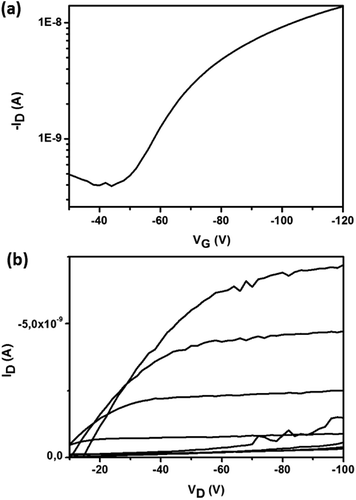 | ||
| Fig. 6 (a) Transfer (at a fixed VD value of 100 V) and (b) output plots (VG was varied from 20 V to −120 V) for compound Bzt-tpa for hole transport. | ||
The results summarized in Table 5 indicate that seven of the studied compounds showed charge transport at negative biases indicating their potential as p-type semiconductors. The results are consistent with the values for the HOMO and LUMO frontier orbitals. All of the HOMO values are around −5.0 eV, i.e., close to the Fermi level of the electrode (gold), but the LUMO levels are far from this latter.
The hole mobilities (λh) are modest, in the range 10−4 to 10−5 cm2 V−1 s−1. Note that a certain dependence with mobility and the donor group used can be found.
In general, the mobility values are in good agreement with the π-conjugation degree derived from the C![[triple bond, length as m-dash]](https://www.rsc.org/images/entities/char_e002.gif) C triple bond stretching frequencies recorded by Raman spectroscopy, indicating that lower ring aromaticity lead to improved charge delocalisation in the structure. Thus, the injected charges are expected to be more easily stabilized for the less aromatic compounds. As a consequence, compound Bzt-thbz having a lower ν(C
C triple bond stretching frequencies recorded by Raman spectroscopy, indicating that lower ring aromaticity lead to improved charge delocalisation in the structure. Thus, the injected charges are expected to be more easily stabilized for the less aromatic compounds. As a consequence, compound Bzt-thbz having a lower ν(C![[triple bond, length as m-dash]](https://www.rsc.org/images/entities/char_e002.gif) C) frequency is a more efficient semiconductor than Bzt-bzth. Finally, Bzt-phe and Bzt-pyr show similar behaviour. However, in this case it can be seen from the optimized structure found by DFT calculations that there is another explanation for this behaviour. In both cases there is a torsion angle between the donor and acceptor groups and this becomes more marked as the number of benzene rings increases (Fig. 2). As a consequence, in Bzt-pyr there is significant torsion that prevents molecular orbital overlapping between neighbour molecules and thus intermolecular charge transport is hindered as a consequence.
C) frequency is a more efficient semiconductor than Bzt-bzth. Finally, Bzt-phe and Bzt-pyr show similar behaviour. However, in this case it can be seen from the optimized structure found by DFT calculations that there is another explanation for this behaviour. In both cases there is a torsion angle between the donor and acceptor groups and this becomes more marked as the number of benzene rings increases (Fig. 2). As a consequence, in Bzt-pyr there is significant torsion that prevents molecular orbital overlapping between neighbour molecules and thus intermolecular charge transport is hindered as a consequence.
In an effort to explain the results, the characteristics of thin films were studied by techniques such as wide-angle X-ray diffraction (WAXRD) and atomic force microscopy (AFM). These two techniques provide information about microstructural regularity and allow a good estimation of the molecular orientation with respect to the gate insulator surface. It is known that the best orientation between the source and drain electrodes occurs when the cofacial π-conjugated molecular planes are aligned perpendicular to the dielectric substrate surface, thus increasing charge transport.30 For this purpose, only vapour-deposited films on preheated (90 °C) HMDS-treated Si/SiO2 substrates were studied.
Comparison of the XRD results for Bzt-tpa, Bzt-cbz and Bzt-phenox (Fig. 7) shows that they are consistent with the OFET parameters. Two peaks can be observed for Bzt-tpa, indicating a polycrystalline film. In contrast, Bzt-cbz and Bzt-phenox were essentially amorphous since Bragg reflections were not detected. A plausible explanation for this finding lies in the fact that the phenylcarbazole and phenylphenoxazine groups are planar but they are perpendicular to the benzotriazole core, thus distorting the planarity and hindering the appropriate self-assembly. As a result, the structures of Bzt-cbz and Bzt-phenox are less crystalline than that of Bzt-tpa, despite its non-planar structure, but the orientation of the benzene rings allows effective self-assembly through π–π stacking.
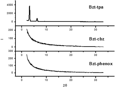 | ||
| Fig. 7 X-ray diffraction scans of vapour-deposited Bzt-tpa, Bzt-cbz and Bzt-phenox at 90 °C on substrates treated with hexamethyldisilazane (HMDS). | ||
The XRD patterns for Bzt-thbz and Bzt-bzth, both including a thiophene ring in their molecular structures, are depicted in Fig. 8. The peak that appears at around 20 degrees is a key factor because it indicates efficient π–π stacking between molecular planes. This peak is only observed in Bzt-thbz but not in Bzt-bzth, which indicates a lower level of crystallinity in the latter. It is important to note the differences observed in samples at 90 °C and at room temperature in the case of Bzt-bzth. In general, it is known that higher temperatures provide better organization of the molecules in the active region, which may improve charge transport within the semiconductor layer. For this reason, an additional peak was observed in the sample at 90 °C when compared with the room temperature sample.
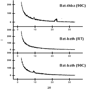 | ||
| Fig. 8 X-ray diffraction scans of vapour-deposited Bzt-thbz and Bzt-bzth (room temperature and 90 °C) on substrates treated with hexamethyldisilazane (HMDS). | ||
On comparing the XRD data for Bzt-pyr and Bzt-phe (Fig. 9) a high intensity peak is observed at around 8 degrees for Bzt-phe being this less intense in the case of Bzt-pyr, which indicates that the crystallinity is enhanced in the former. The high level of torsion in Bzt-pyr when compared to Bzt-phe in the optimized structure is another explanation for this finding as this torsion may hinder intermolecular crystal packing.
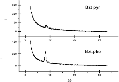 | ||
| Fig. 9 X-ray diffraction scans of vapour-deposited Bzt-phe and Bzt-pyr (90 °C) on substrates treated with hexamethyldisilazane (HMDS). | ||
Thin films were also characterized by tapping mode AFM. The most crucial interface in a field-effect transistor is the dielectric–semiconductor interface, where charge transport takes place. Although that interface is buried, AFM imaging is often used to correlate film microstructures with charge transport. The morphologies of the vapour-deposited Bzt-phe, Bzt-thbz and Bzt-tpa, which are the compounds rendering the best mobilities, are in a good agreement with the XRD data. In all cases organized aggregates with well-defined fibres were obtained, and this fact directly influences the electrical behaviour (Fig. 10).
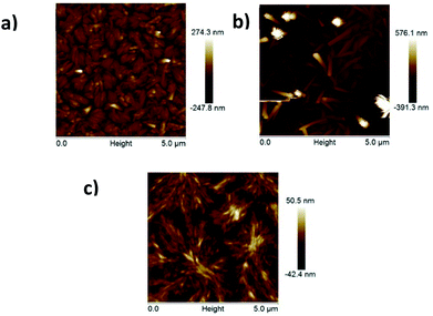 | ||
| Fig. 10 AFM images of Bzt-phe HMDS 90 °C (a) Bzt-thbz HMDS 90 °C (b) Bzt-tpa HMDS 90 °C (c). Image size: 5 × 5 μm. | ||
In summary, all of the techniques employed in this study (DFT calculations, Raman spectroscopy, XRD and AFM) allow the establishment of useful relationships between the semiconductor electronic and molecular structures and the properties as organic semiconductors in OFETs for the different 2H-benzo[d][1,2,3]triazole derivatives.
Conclusions
In the present work, 4,7-bis(arylethynyl)-2H-benzo[d][1,2,3]triazole derivatives (Bzt-Ar) were tested as semiconductors in OFETs. The electronic and molecular structures of the semiconductors were tuned by maintaining the same central acceptor group, namely a benzotriazole with two trifluoromethyl groups to increase its acceptor ability, and including different donor groups. A total of ten different donor groups with varying electron donating strengths were evaluated.The organic semiconductors were characterized by DFT calculations, X-ray diffraction, AFM, and FT-Raman spectroscopy. Analysis of the data obtained by the optical and vibrational techniques indicate that molecular planarity and efficient intramolecular charge transfer between acceptor and donor groups have an impact on their electrical properties.
Although the mobility values obtained here are modest, with values around 10−4 cm2 V−1 s−1, this study demonstrates for the first time the applicability of benzotriazole derivatives in organic electronics. Future modifications of these derivatives could improve their mobility and their applicability. Due to an adequate alignment between the energy levels of the semiconductors and the used electrodes, all of the semiconductors studied here act as p-type materials. The obtained results indicate that compounds Bzt-phe, Bzt-thbz and Bzt-tpa are the most promising candidates as organic semiconductors.
Finally, it is worth noting the multifunctionality of 2H-benzo[d][1,2,3]triazole derivatives, both as waveguide materials, which was previously described, and as p-type semiconductors in OFETs.
Experimental section
All reagents were used as purchased. Reactions with air-sensitive materials were carried out under an argon atmosphere. Flash chromatography was perfomed using silica gel (Merck, Kieselgel 60, 230–240 mesh or Scharlau 60, 230–240 mesh). Analytical thin layer chromatography (TLC) was performed using aluminium-coated Merck Kieselgel 60 F254 plates.Cyclic voltammetry measurements were performed on a μ-Autolab ECO-Chemiepotentiostat using a glassy carbon working electrode, Pt counter electrode and Ag/AgCl reference electrode. The experiments were carried out under argon, in CHCl3, with Bu4NPF6 as supporting electrolyte (0.1 mol L−1). The scan rate was 50 mV s−1.
UV-vis spectra were recorded on a Varian Cary model 5000 UV-vis-NIR spectrophotometer using standard quartz cells of 1 cm width and solvents of spectroscopic grade.
Theoretical calculations were carried out in the framework of density functional theory (DFT) using the B3LYP functional31,32 and the 6-31G(d,p) basis set33,34 as implemented in the Gaussian 09 programme.35 Geometry optimizations were performed using the medium-sized 6-31G(d,p) basis set and frequency calculations were performed to confirm the nature of ground state stationary points. The reorganization energies were calculated through the relevant points on the potential energy surfaces.36,37 Ground state redox potentials were calculated from the difference in Gibbs free energy between neutral molecules and oxidized radical ions in solutions using the CPCM solvation model.38
FT-Raman spectra with 1064 nm excitation were recorded using an FT Raman accessory kit (RamIl) on a Bruker Vertex 70 FT-IR interferometer and a continuous-wave Nd:YAG laser. A germanium detector operating at liquid-nitrogen temperature was used and the Raman scattering radiation was collected in a back-scattering configuration with a 4 cm−1 spectral resolution. An average of 1000 scans were used in the reported spectra.
All top-contact/bottom-gate OFETs were fabricated with the benzotriazole derivatives Bzt-Ar as the active layer. Gate dielectrics (p-doped Si wafers with 300 nm thermally grown SiO2 layers) were functionalized either with a hexamethyldisilazane (HMDS) or octadecyltrichlorsilane (OTS) self-assembled monolayer. The capacitance of the 300 nm SiO2 gate insulator was 10 nF cm−2. Prior to surface functionalization, the wafers were cleaned by immersing them twice for 30 seconds each in EtOH with sonication, drying with a stream of N2 and treating with UV-ozone for 10 min. The cleaned silicon wafers were treated with hexamethyldisilazane (HMDS) by exposing them to HMDS vapour at room temperature in a closed air-free container under argon for a week, or were treated with octadecyltrichlorosilane (OTS) by immersion in a 3.0 mM humidity-exposed solution of OTS in hexane for 1 hour following a previously reported procedure.39 Following OTS deposition, the substrates were sonicated with hexane, acetone, and finally with ethanol, and dried with an N2 stream. The semiconductors were then vapour-deposited on preheated substrates.
After semiconductor deposition, the films were analysed by AFM and XRD techniques. X-ray diffraction patterns were recorded on a Bruker D8 Discover A25 diffractometer by employing a scanning range of 2θ = 2–33° with CuKα1 X-ray radiation. AFM images were registered in tapping mode on an atomic force microscope (Veeco Instruments MultiModeNanoscope V). OFET devices were completed by vapour deposition of gold electrodes through a shadow mask to define devices with various channel lengths and channel widths. Devices were characterized under vacuum and ambient conditions in an EB-4 Everbeing probe station with a 4200-SCS/C Keithley semiconductor characterization system.
Conflicts of interest
There are no conflicts to declare.Acknowledgements
This work was financially supported by MINECO of Spain (project CTQ2014-53600-R and CTQ2015-66897-P) and UCLM (GI20163531). I. Torres is indebted to MEC for an FPU studentship. I. Arrechea acknowledges MINECO of Spain for a FPI fellowship. Technical support from the High Performance Computing Service of the University of Castilla-La Mancha and the Vibrational Spectroscopy Laboratory at Research Support Central Services (SCAI) at the University of Málaga are gratefully acknowledged.Notes and references
- (a) Q. Tang, L. Jiang, Y. Tong, H. Li, Y. Liu, Z. Wang, W. Hu, Y. Liu and D. Zhu, Adv. Mater., 2008, 20, 2947–2951 CrossRef; (b) T. Lei and J. Pei, J. Mater. Chem., 2012, 22, 785–798 RSC; (c) Y. Zhou, L. Wang, J. Wang, J. Pei and Y. Cao, Adv. Mater., 2008, 20, 3745–3749 CrossRef; (d) Y. Yao, H. Dong and W. Hu, Adv. Mater., 2016, 28, 4513–4523 CrossRef PubMed; (e) Q. Tai and F. Yan, Adv. Mater., 2017, 29, 1700192 CrossRef PubMed.
- (a) B. A. D. Neto, P. H. P. R. Carvalho and J. R. Correa, Acc. Chem. Res., 2015, 48, 1560–1569 CrossRef PubMed; (b) T. Someya, Z. Bao and G. G. Malliaras, Nature, 2016, 540, 379–385 CrossRef PubMed; (c) D. Chen and Q. Pei, Chem. Rev., 2017, 117, 11239–11268 CrossRef PubMed; (d) C. García-Astrain, C. Chen, M. Burón, T. Palomares, A. Eceiza, L. Fruk, M. A. Corcuera and N. Gabilondo, Biomacromolecules, 2015, 14, 1302–1310 Search PubMed.
- Y. Wu and W. Zhu, Chem. Soc. Rev., 2013, 42, 2039–2058 RSC.
- C. Wang, H. Dong, V. Hu, Y. Liu and D. Zhu, Chem. Rev., 2012, 112, 2208–2267 CrossRef PubMed.
- F. J. M. Hoeben, P. Jonkheijm, E. W. Meijer and A. P. H. Schenning, Chem. Rev., 2005, 105, 1491–1546 CrossRef PubMed.
- F. S. Kim, G. Ren and S. A. Jenekhe, Chem. Mater., 2011, 23, 682–732 CrossRef.
- A. L. Briseno, S. C. B. Mannsfeld, S. A. Jenekhe, Z. Bao and Y. Xia, Mater. Today, 2008, 11, 38–47 CrossRef.
- L. Jiang, H. Dong and W. J. Hu, Mater. Chem., 2010, 20, 4994–5007 RSC.
- (a) Y. Zhou, W. Liu, Y. Ma, H. Wang, L. Qi, Y. Cao, J. Wang and J. Pei, J. Am. Chem. Soc., 2007, 129, 12386–12387 CrossRef PubMed; (b) A. L. Briseno, S. C. B. Mannsfeld, C. Reese, J. Hancook, Y. Xiong, S. A. Jenekhe, Z. Bao and Y. Xia, Nano Lett., 2007, 7, 2847–2853 CrossRef PubMed; (c) L. Jiang, Y. Fu, H. Li and W. Hu, J. Am. Chem. Soc., 2008, 130, 3937–3941 CrossRef PubMed; (d) J. Yang, D. Yan and T. S. Jones, Chem. Rev., 2015, 115, 5570–5603 CrossRef PubMed.
- (a) W. Huang, B. Yang, J. Sun, B. Liu, J. Yang, Y. Zou, J. Xiiong, C. Zhou and Y. Gao, Org. Electron., 2014, 15, 1050–1055 CrossRef; (b) Y. Huang, J. Sun, J. Zhang, S. Wang, H. Huang, J. Zhang, D. Yan, Y. Gao and J. Yang, Org. Electron., 2016, 36, 73–81 CrossRef.
- J. A. Rogers, Z. Bao, K. Baldwin, B. Dodabalapur, V. Crone, R. Raju, V. Kuck, H. Katz, J. Amundson, J. Ewing and P. Drzaic, Proc. Natl. Acad. Sci. U. S. A., 2001, 98, 4835–4840 CrossRef PubMed.
- G. Gelinck, P. Heremans, K. Nomoto and T. D. Anthopoulos, Adv. Mater., 2010, 22, 3778–3798 CrossRef PubMed.
- Y. Guo, G. Yu and Y. Liu, Adv. Mater., 2010, 22, 4427–4447 CrossRef PubMed.
- C. Reese and Z. Bao, Mater. Today, 2007, 10, 20–27 CrossRef.
- T. Hasegawa and J. Takeya, Sci. Technol. Adv. Mater., 2009, 10, 024314 CrossRef PubMed.
- (a) D. Patel, F. Fude, Y. Ohnishi, K. Abboud, S. H. Hirata, K. S. Schanze and J. R. Reynolds, J. Am. Chem. Soc., 2012, 134, 2599–2612 CrossRef PubMed; (b) B. Liu, S. Ye, Y. Zou, B. Peng, Y. He and H. Zhou, Chem. Phys., 2011, 212, 1439–1496 Search PubMed; (c) Y. Dong, W. Cal, M. Wang, Q. Li, L. Yilg, F. Huang and Y. Cao, Org. Electron., 2013, 14, 2459–2467 CrossRef; (d) Y. Dong, W. Cai, X. Hu, C. Zhong, F. Huang and Y. Cao, Polymer, 2012, 53, 1465–1471 CrossRef.
- I. Torres, J. R. Carrillo, A. Díaz-Ortiz, R. Martín, M. V. Gómez, L. Stegemann, C. A. Strassert, J. Orduna, J. Buendía, E. E. Greciano, J. S. Valera, E. Matesanz, L. Sánchez and P. Prieto, RSC Adv., 2016, 6, 36544–36553 RSC.
- I. Torres, A. Díaz-Ortiz, L. Sánchez, J. Orduna, M. J. Blesa, J. R. Carrillo and P. Prieto, Dyes Pigm., 2017, 142, 212–225 CrossRef.
- (a) Y. Liu, G. Xie, K. Wu, Z. Luo, T. Zhou, X. Zeng, J. Yu, S. Gong and C. Yang, J. Mater. Chem. C, 2016, 4, 4402–4407 RSC; (b) C. Quinton, S. Thiery, O. Jeannin, D. Tondelier, B. Geffroy, E. Jacques, J. Rault-Berthelot and C. Poriel, ACS Appl. Mater. Interfaces, 2017, 9, 6194–6206 CrossRef PubMed.
- X. Lu, S. Fan, J. Wu, X. Jia, Z. S. Wang and G. Zhou, Org. Lett., 2013, 15, 3530–3533 CrossRef PubMed.
- R. Ponce, H. Herrera, R. Blanco, H. Huang, A. Facchetti, T. J. Marks, Y. Zheng and J. L. Segura, J. Am. Chem. Soc., 132, 8440–8452 Search PubMed.
- M. C. Ruiz Delgado, E. G. Kim, D. A. da Silva and J. L. Bredas, J. Am. Chem. Soc., 2010, 132, 3375–3387 CrossRef PubMed.
- (a) M. Y. Kuo, H. Y. Chen and I. Chao, Chem.–Eur. J., 2007, 13, 4750–4758 CrossRef PubMed; (b) O. Kwon, V. Coropceanu, N. E. Gruhn, J. C. Durivage, J. G. Laquindanum, H. G. Katz, J. Cornil and J. L. Brédas, J. Chem. Phys., 2004, 120, 8186–8194 CrossRef PubMed; (c) H. Y. Chen and I. Chao, Chem. Phys. Lett., 2005, 401, 539–545 CrossRef.
- D. A. da Silva, E. G. Kim and J. L. Bredas, Adv. Mater., 2005, 17, 1072–1076 CrossRef.
- Y. M. Sun, Y. Q. Ma, Y. Q. Liu, Y. Y. Liu, Y. Y. Lin, Z. Y. Wang, Y. Wang, C. A. Di, K. Xiao, X. M. Chen, W. F. Qiu, B. Zhang, G. Yu, W. P. Hu and D. B. Zhu, Adv. Funct. Mater., 2006, 16, 426–432 CrossRef.
- R. Ponce, J. Casado, V. Hernández, J. T. López, P. Viruela, E. Ortí, K. Takimiya and T. Otsubo, Angew. Chem., Int. Ed., 2007, 46, 9057–9061 CrossRef PubMed.
- G. Zerbi, M. Veronelli, S. Martina, A. D. Schlüter and G. Wegner, Adv. Mater., 1994, 6, 385–388 CrossRef.
- S. M. Size and M. K. Lee. Semiconductor devices: Physics and Technology, Wiley, New York, 3 edn, 2012 Search PubMed.
- R. Ponce, A. Facchetti and T. J. Marks, Chem. Rev., 2010, 110, 205–239 CrossRef PubMed.
- Y. Sun, Y. Liu and D. Zhu, J. Mater. Chem., 2005, 15, 53–65 RSC.
- C. Lee, W. Yang and R. G. Parr, Phys. Rev. B, 1988, 37, 785–789 CrossRef.
- A. D. Becke, J. Chem. Phys., 1993, 98, 1372–1377 CrossRef.
- P. C. Hariharan and J. A. Pople, Theor. Chim. Acta, 1973, 28, 213–222 CrossRef.
- W. J. Hehre, R. Ditchfield and J. A. Pople, J. Chem. Phys., 1972, 56, 2257–2261 CrossRef.
- M. J. Frisch, G. W. Trucks, H. B. Schlegel, G. E. Scuseria, M. A. Robb, J. R. Cheeseman, G. Scalmani, V. Barone, B. Mennucci, G. A. Petersson, H. Nakatsuji, M. Caricato, X. Li, H. P. Hratchian, F. A. Izmaylov, J. Bloino, G. Zheng, J. L. Sonnenberg, M. Hada, M. Ehara, K. Toyota, R. Fukuda, J. Hasegawa, M. Ishida, T. Nakajima, Y. Honda, O. Kitao, H. Nakai, T. Vreven, J. A. Montgomery, J. E. Peralta, F. Ogliaro, M. Bearpark, J. J. Heyd, E. Brothers, K. N. Kudin, V. N. Staroverov, R. Kobayashi, J. Normand, K. Raghavachari, A. Rendell, J. C. Burant, S. S. Iyengar, S. J. Tomasi, M. Cossi, N. Rega, N. J. Millam, M. Klene, J. E. Knox, J. B. Cross, V. Bakken, C. Adamo, J. Jaramillo, R. Gomperts, R. E. Stratmann, O. Yazyev, A. J. Austin, R. Cammi, C. Pomelli, J. W. Ochterski, R. L. Martin, K. Morokuma, V. G. Zakrzewski, G. A. Voth, P. Salvador, J. J. Dannenberg, S. Dapprich, A. D. Daniels, O. Farkas, J. B. Foresman, J. V. Ortiz, J. Cioslowski and D. J. Fox, Gaussian 09, Revision A.1, Gaussian, Inc., Wallingford CT, 2009 Search PubMed.
- M. Malagoli and J. L. Brédas, Chem. Phys. Lett., 2000, 327, 13–17 CrossRef.
- J. L. Brédas, D. Beljonne, V. Coropceanu and J. Cornil, Chem. Rev., 2004, 104, 4971–5004 CrossRef PubMed.
- (a) A. Klamt and G. Schürmann, J. Chem. Soc., Perkin Trans. 2, 1993, 799–805 RSC; (b) J. Andzelm, C. Kölmel and A. Klamt, J. Chem. Phys., 1995, 103, 9312–9320 CrossRef; (c) V. Barone and M. Cossi, J. Phys. Chem. A, 1998, 102, 1995–2001 CrossRef; (d) M. Cossi, N. Rega, G. Scalmani and V. J. Barone, Comput. Chem., 2003, 24, 669–681 CrossRef PubMed.
- H. Li, F. S. Kim, G. Ren, E. C. Hollenbeck, S. Subramaniyan and S. A. Jenekhe, Angew. Chem., Int. Ed., 2013, 52, 5513–5517 CrossRef PubMed.
Footnote |
| † Electronic supplementary information (ESI) available. See DOI: 10.1039/c8ra03246g |
| This journal is © The Royal Society of Chemistry 2018 |

