 Open Access Article
Revealing the role of oxygen vacancies on the phase transition of VO2 film from the optical-constant measurements
Lele Fan ab,
Xiangqi Wangc,
Feng Wanga,
Qinfang Zhang
 *a,
Lei Zhua,
Qiangqiang Meng
 a,
Baolin Wangd,
Zengming Zhang
 c and
Chongwen Zou*b
aKey Laboratory for Advanced Technology in Environmental Protection of Jiangsu Province, Yancheng Institute of Technology, Yancheng 224051, P. R. China. E-mail: qfangzhang@gmail.com
bNational Synchrotron Radiation Laboratory, University of Science and Technology of China, Hefei, 230029, P. R. China. E-mail: czou@ustc.edu.cn
cDepartment of Physics, University of Science and Technology of China, Hefei, 230026, P. R. China
dSchool of Physical Science and Technology, Nanjing Normal University, Nanjing 210023, P. R. China
First published on 24th May 2018
Abstract
Vanadium dioxide (VO2) material shows a distinct metal–insulator transition (MIT) at the critical temperature of ∼340 K. Similar to other correlated oxides, the MIT properties of VO2 is always sensitive to those crystal defects such as oxygen vacancies. In this study, we investigated the oxygen vacancies related phase transition behavior of VO2 crystal film and systematically examined the effect of oxygen vacancies from the optical constant measurements. The results indicated that the oxygen vacancies changed not only the electron occupancy on V 3d–O 2p hybrid-orbitals, but also the electron–electron correlation energy and the related band gap, which modulated the MIT behavior and decreased the critical temperature resultantly. Our work not only provided a facile way to modulate the MIT behavior of VO2 crystal film, but also revealed the effects of the oxygen vacancies on the electronic inter-band transitions as well as the electronic correlations in driving this MIT process.
Introduction
Transition metal oxide materials have been widely investigated due to their specific properties such as the giant magneto-resistance, superconductivity and 2D electronic gas behavior.1–3 It is suggested that the function of transition metal oxide is usually associated with the oxygen stoichiometry and the properties can be greatly modulated by introducing oxygen vacancies.4–7 As a typical correlated oxide material, vanadium dioxide (VO2) has been broadly studied due to its unique metal–insulator phase transition (MIT) characteristics. During its phase transition, the resistance undergoes a large change up to 5 orders of magnitude and the infrared transmittance shows a pronounced switching behavior.8 These excellent characteristics of VO2 material make it suitable for many promising applications in various fields such as smart window, ultra-fast optical switch, infrared detectors, phase-change material and thermal sensor.9–16 However, the relatively high critical transition temperature (Tc ∼ 340 K) of VO2 material limits its practical applications.As typical point defects in crystal lattices, oxygen vacancies have been widely investigated in VO2 material, which are suggested to be effective to decrease the critical temperature or even stabilized the metallic state at room temperature.17–19 While till now, it still remains some open questions about the real effects of oxygen vacancies if considering the complex valence states of V atoms and the diffusion/reaction routes of O atoms in the crystal lattices.19–23 Positron annihilation technology was supposed to be an ideal tool to directly detect the defect types in material, the insensitive feature to oxygen defect made it difficult to analyze the role of oxygen vacancies. X-ray Photoelectron Spectroscopy (XPS) was usually performed to determine the atomic stoichiometry, while its surface-sensitive property was not suitable to obtain the deeper layer or bulk information. Secondary Ion Mass Spectrometry (SIMS) was an effective way to detect the atomic concentration from the surface to deeper layer, which was always used to detect the atomic vacancies. But this method could not supply the related electronic and energy band structure, which should be modulated by the point defects in the crystal lattices.
In fact, optical conductivity measurements have been demonstrated to be a suitable method in analyzing the electronic structure of material.24–32 For example, Basov group revealed the Mott transition property of VO2 by using optical conductivity and explained the peaks in optical conductivity curve according to electron transition.24,25 Lee used optical conductivity method to investigate the electron correlation in W–VO2 film.26 Wolf group studied the electronic structure of VO2 under strained state from optical constant view.28 However, till now, few studies were conducted to examine the oxygen vacancies involved MIT behavior from the point view of optical conductivity.
In the present work, we conducted the optical constant measurements and systematically investigated the role of oxygen vacancies on the MIT process of VO2 crystal film. By fitting the ellipsometry parameters, temperature-dependent optical constant of VO2 films were obtained and the extinction coefficient of VO2 showed abruptly changing in infrared range at Tc. The optical conductivity of VO2 film was obtained by calculating the optical constant (n, k), and the corresponding band structure were extracted. Combined with the first-principle calculation, the role of oxygen vacancies on VO2 was discussed.
Experimental section
VO2 films deposition
The VO2 films were prepared on MgF2 (110) single crystal substrates by a rf-plasma assisted oxide MBE instrument with base pressure better than 3 × 10⁻⁹ torr. During the deposition, the growth temperature was kept at 530 °C. For VO2 on MgF2 (110) with good stoichiometry, the oxygen flux was kept at 3.6 sccm, while the oxygen vacancies were induced by decreasing the oxygen flux to 3.0 sccm.Sample characterization
The X-Ray Diffraction (XRD) relative measurement was performed on Shanghai Synchrotron Radiation Facility (SSRF) 14B beamline. The BL14B shows the energy resolution (ΔE/E) of 1.5 × 10⁻⁴ at 10 keV and the beam size of 0.4 mm × 0.3 mm with the photo flux of up to 2 × 10¹² phs s−1 at 10 keV. The resistances of films were measured by four-probe testing system with a variable-temperature platform. The variable-temperature ellipsometer (J. A. Woollam Co. Inc. M-2000U) was used to measure the optical constant of VO2 films with an incident angle of 70° and 0.7–5 eV photonic energy.Theoretical calculations
The Vienna Ab initio Simulation Package (VASP) was performed to simulate the geometric and electronic properties with 2 × 2 × 2 primitive unit cells. The all electron projector augmented wave (PAW) model and Perdew–Burke–Ernzerhof (PBE) exchange–correlation functional were employed. The generalized gradient approximation (GGA)+U method was performed to deal with the 3d electron in VO2. We adopted U = 4 eV and J = 0.68 eV for Hund's exchange interaction.21,22,33–36 A kinetic energy cutoff of 400 eV was used for the plane-wave expansion of the electronic wave function. The electronic structure of VO2 induced by oxygen vacancies was calculated by just deleting one oxygen atom in the supercell, with the lowest total energy.Results and discussion
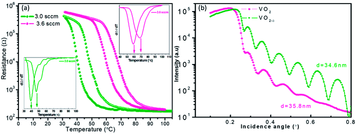
Fig. 1a shows the resistances of VO2 films as the function of temperature. Two samples were measured, one was the pure VO2 sample with ideal atomic stoichiometry and the other one was the oxygen vacancies involved sample. It was observed that as the oxygen vacancies introducing, the R–T curve shift towards the lower temperature direction clearly, and the good metal–insulator transition behavior was still maintained. In previous literature,19,20 the oxygen vacancies reduced the critical temperature at the cost of weakening phase transition behavior, but not occurred in our present work. In order to extract the Tc values, dR/dT curves were plotted in the inset of Fig. 1a. It was observed that the stoichiometric VO2 film showed the Tc value of 67 °C, while the film with oxygen vacancies had the lower Tc of 47 °C. According to previous literatures,18,29,30 both oxygen vacancies and interfacial strain could influence the critical temperature for the epitaxial films. While normally the interfacial strain was closely associated with the film thickness. For our current experiment, the two tested film samples should have almost the same thickness values according to the crystal oscillator monitor during the film growth. | ||
| Fig. 1 Thermal hysteresis loops of VO2 and VO2−δ films (a), inset shows the differential curve of R–T, XRR curves of VO2 and VO2−δ with the 10 keV X-ray incidence (b). | ||
The detailed thickness characterization by synchrotron based X-ray reflectivity (XRR) measurement also confirmed the film thickness information as shown in Fig. 1b. In general, XRR was a non-destructive and non-contacted technique, which was suitable for thickness determination in the range of 2–200 nm with good precision. The thickness of the tested film sample can be evaluated according to the interfacial interference equation:  . Where d is the thickness of film, θm θn is diffraction angle, λ is the X-ray wavelength, and m or n means the m-th or n-th interface order. Fig. 1b showed the periodic oscillation peaks for these two films, indicating the smooth surfaces of the obtained samples with high quality. Based on the XRR curves, the thickness of VO2 and VO2−δ were calculated to be 35.8 nm, 34.6 nm, respectively. Since these two films showed almost the same thickness values, the influence of interfacial strain should be at the similar level. Thus the distinct difference of the critical temperatures for these two films should be mainly due to the presence of oxygen vacancies.
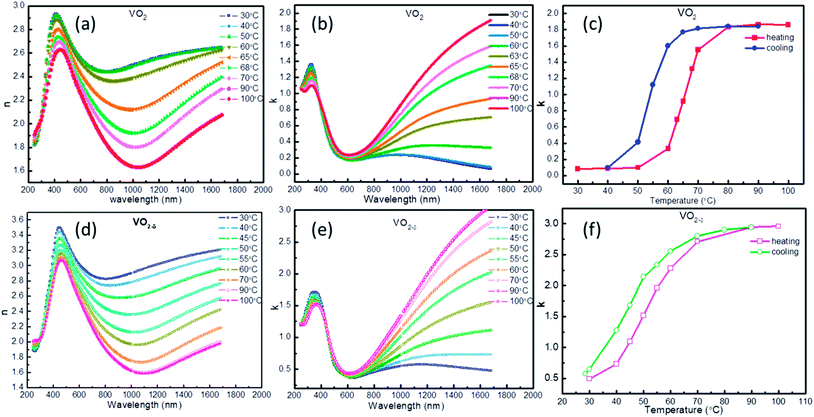
The temperature dependent optical constants for the above two VO2/MgF2 (110) samples were obtained by fitting ellipsometry parameter with Kramers–Kronig consistent. During the fitting process, the effect from the MgF2 substrate was subtracted. Fig. 2a, b, d and e showed the temperature-dependent n (real part of Refractive index) and k (imaginary part of Refractive index) value for VO2 and VO2−δ films, which was consistent with previous reports.20,31,32 Both the n or k values appear temperature-independent in visible spectrum, however, the dispersion behaviors of optical constant for VO2 and VO2−δ films are clearly observed in near IR range. Since the n represents the refraction ability of material to incidence light, the dispersion behavior of VO2 films will be useful for IR camouflage application. For example, by covering VO2 on some material and through controlling the surface temperature of VO2, the VO2 will appear the same optical property as that of surrounding environment and achieve IR camouflage. On the other way, the k means the extinction coefficient and indicates the absorption of light. VO2 films appear enormous variation of k value in IR range during heating and cooling process, implying the usage in energy-saving field. To better observe the change of k as temperature, we plotted the k–T curves at 1680 nm as shown in Fig. 2c and f. The k–T curves appear the similar behavior as that of R–T curves, hysteresis property and abrupt changing at critical temperature.
 | ||
| Fig. 2 The n (a and d) and k (b and e) of VO2 and VO2−δ films as a function of wavelength under different temperature, the k–T curves (c and f) of VO2 and VO2−δ. | ||
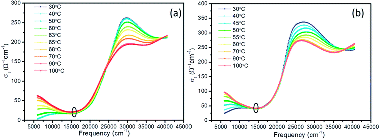
Based on the n and k, the optical conductivity (σ) of VO2 films can be obtained according to the formula:  ,24 where ε2 means the imaginary part of dielectric constant, and ε2 = 2nkε0, ω means the photonic frequency. The optical conductivity reflects the electron transition between conductivity band and valence band. In Fig. 3a and b, the optical conductivity values as the function of temperature for VO2 and VO2−δ in wavenumber coordinate are plotted. Obvious isosbestic points (equal conductivity) related to the fingerprint in doped Mott insulator materials are observed,24 which means the electron–electron correlation could greatly influence metal or insulator property of material. Moreover, as the introduction of oxygen vacancies, the isosbestic point shifts towards low wavenumber from ∼15
![[thin space (1/6-em)]](https://www.rsc.org/images/entities/char_2009.gif) 400 to ∼14
400 to ∼14![[thin space (1/6-em)]](https://www.rsc.org/images/entities/char_2009.gif) 400 cm−1. It is suggested that oxygen vacancies in VO2 lattice will weaken the interaction between V ion and O ion and decrease the electron–electron correlation, resulting the weakened interactions between incident photonic and electron.
400 cm−1. It is suggested that oxygen vacancies in VO2 lattice will weaken the interaction between V ion and O ion and decrease the electron–electron correlation, resulting the weakened interactions between incident photonic and electron.
 | ||
| Fig. 3 Optical conductivity of VO2 (a) and VO2–δ (b) films as a function of wavenumber at representative temperature. | ||
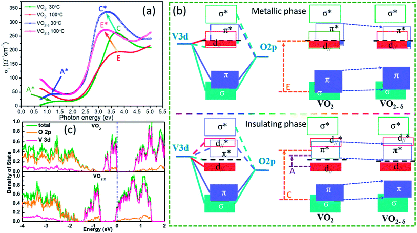
In Fig. 4a, we plot the optical conductivity of VO2 and VO2−δ before and after MIT process and compare the relative shifts. Except the isosbestic point, several peaks emerge, which are attributed to the electron transitions across the energy bands. This peaks can also be understand based on the classic Goodenough model for VO2 as shown in Fig. 4b.37 According to crystal-field theory, the 3d energy levels of V ion are split into triplet degenerate low-energy t2g band and double degenerate high-energy eσg band, where σ represents the symmetry of V–O bonds. In oxygen octahedral environment, the different V–O bond lengths in equatorial and apical planes further cause t2g band splitting into double degenerate eπg bands and single a1g band. The eσg bands and eπg bands will hybridize with O 2p band respectively, which forms the low-energy bonding π, σ bands and high-energy anti-bonding π*, σ* bands. The a1g orbital is no bonding with O 2p level, and the orbital wave function of a1g is parallel to c axis of R–VO2 (usually named as d∥ orbital). Accordingly, based on this band structures, the peaks A and peak C in Fig. 4a are assigned to be the electron transitions from occupied d∥ to conductivity π* band and O 2p to π* band, respectively.25,32 In addition, the band gap of pure VO2 film estimated from Fig. 4a is close to 0.65 eV, which is quite consistent with the reported standard band gap of VO2.21 While for the oxygen vacancies involved insulator state at room temperature, the peak A moves to low energy direction as peak A*, reflecting a narrower band gap formation. This effect will decrease the energy barrier during the insulator to metal transition, which is favor for decreasing the phase transition temperature. While for the metallic states at 100 °C, if oxygen vacancies is involved, the E peak moves towards low energy direction to peak E*, implying the π band shifting down. Supposing d∥ band is static, which is reasonable as the d∥ band only depended by interfacial strain or crystal constant. The shifting down of π* band will increase the overlap between π* band and d∥ band (seen in Fig. 4b), and the itinerant electrons in the d∥ band may partially transfer to the π* band, which decrease the electron–electron correlation and stabilize metallic state.
To further confirming the effect of oxygen vacancies in VO2 lattice, we also carry out first principle calculations based on density function theory as shown in Fig. 4c. The basic calculations are performed in the supercell with 2 × 2 × 2 primitive unit cells for the monoclinic VO2 consisting of 96 atoms and for oxygen vacancy calculation just with one oxygen atom been deleted. For pure VO2, we can clearly see an obvious band gap (∼0.6 eV) between conduction band and valence band. In the partial density of state, the overlap between V 3d and O 2p is observed, indicating strong hybridization. However, in oxygen vacancies involved VO2 crystal, the Fermi level is occupied by V 3d electron, indicating the metallic state formation.
Conclusions
In summary, we investigated the role of oxygen vacancies on VO2 phase transition from optical constant measurements. By fitting ellipsometry parameter, electronic band structures for the pure VO2 crystal and the oxygen deficient VO2−δ crystal were extracted. It was suggested that the oxygen vacancies changed the electron orbital occupancy and band structures, which further decreased the critical temperature. Theory calculations also certified a conduction band emerged as oxygen vacancies emergence. Our current research provided a novel way to detect oxygen vacancies and understand the role of oxygen vacancies in the MIT process of VO2 or other transition metal oxides.Conflicts of interest
There are no conflicts to declare.Acknowledgements
Authors are grateful to Prof. J. Jiang (Jun Jiang) of University of Science and Technology of China for helpful discussion about theory calculation. This work was supported by the National Natural Science Foundation of China (11704325, 11474246, 11774178, 11574279, 11604288, U1432249, 11750110415), the Natural Science Foundation of Jiangsu Province (No. BK20170473, BK20160061). The authors also acknowledge the supporting from Shanghai Synchrotron Radiation Facility.References
- I. M. Miron, K. Garello, G. Gaudin, P.-J. Zermatten, M. V Costache, S. Auffret, S. Bandiera, B. Rodmacq, A. Schuhl and P. Gambardella, Nature, 2011, 476, 189–194 CrossRef PubMed.
- H. Y. Hwang, Y. Iwasa, M. Kawasaki, B. Keimer, N. Nagaosa and Y. Tokura, Nat. Mater., 2012, 11, 103–113 CrossRef PubMed.
- A. F. Santander-Syro, O. Copie, T. Kondo, F. Fortuna, S. Pailhès, R. Weht, X. G. Qiu, F. Bertran, A. Nicolaou, A. Taleb-Ibrahimi, P. Le Fèvre, G. Herranz, M. Bibes, N. Reyren, Y. Apertet, P. Lecoeur, A. Barthélémy and M. J. Rozenberg, Nature, 2011, 469, 189–193 CrossRef PubMed.
- L. Liang, K. Li, C. Xiao, S. Fan, J. Liu, W. Zhang, W. Xu, W. Tong, J. Liao, Y. Zhou, B. Ye and Y. Xie, J. Am. Chem. Soc., 2015, 137, 3102–3108 CrossRef PubMed.
- S. Kim, S. Choi and W. Lu, ACS Nano, 2014, 8, 2369–2376 CrossRef PubMed.
- C. Gao, Q. Meng, K. Zhao, H. Yin, D. Wang, J. Guo, S. Zhao, L. Chang, M. He, Q. Li, H. Zhao, X. Huang, Y. Gao and Z. Tang, Adv. Mater., 2016, 28, 6485–6490 CrossRef PubMed.
- W. Xue, G. Liu, Z. Zhong, Y. Dai, J. Shang, Y. Liu, H. Yang, X. Yi, H. Tan, L. Pan, S. Gao, J. Ding, X. H. Xu and R. W. Li, Adv. Mater., 2017, 29, 1702162 CrossRef PubMed.
- F. J. Morin, Phys. Rev. Lett., 1959, 3, 34–36 CrossRef.
- J. Zhou, Y. Gao, Z. Zhang, H. Luo, C. Cao, Z. Chen, L. Dai and X. Liu, Sci. Rep., 2013, 3, 03029 CrossRef PubMed.
- W. Huang, X. Yin, C. Huang, Q. Wang, T. Miao and Y. Zhu, Appl. Phys. Lett., 2010, 96, 261908 CrossRef.
- T. Driscoll, H.-T. Kim, B.-G. Chae, B.-J. Kim, Y.-W. Lee, N. M. Jokerst, S. Palit, D. R. Smith, M. Di Ventra and D. N. Basov, Science, 2009, 325, 1518–1521 CrossRef PubMed.
- Z. Li, Z. Hu, J. Peng, C. Wu, Y. Yang, F. Feng, P. Gao, J. Yang and Y. Xie, Adv. Funct. Mater., 2014, 24, 1821–1830 CrossRef.
- Z. Yang, C. Ko and S. Ramanathan, Annu. Rev. Mater. Res., 2011, 41, 337–367 CrossRef.
- Y.-H. Han, K.-T. Kim, H.-J. Shin, S. Moon and I.-H. Choi, Appl. Phys. Lett., 2005, 86, 254101 CrossRef.
- X. Tan, T. Yao, R. Long, Z. Sun, Y. Feng, H. Cheng, X. Yuan, W. Zhang, Q. Liu, C. Wu, Y. Xie and S. Wei, Sci. Rep., 2012, 2, 466 CrossRef PubMed.
- S. Cueff, D. Li, Y. Zhou, F. J. Wong, J. A. Kurvits, S. Ramanathan and R. Zia, Nat. Commun., 2015, 6, 8636 CrossRef PubMed.
- L. L. Fan, S. Chen, G. M. Liao, Y. L. Chen, H. Ren and C. W. Zou, J. Phys.: Condens. Matter, 2016, 28, 255002 CrossRef PubMed.
- J. Jeong, N. Aetukuri, T. Graf, T. D. Schladt, M. G. Samant and S. S. P. Parkin, Science, 2013, 339, 1402–1405 CrossRef PubMed.
- J. Zhang, Z. Zhao, J. Li, H. Jin, F. Rehman, P. Chen, Y. Jiang, C. Chen, M. Cao and Y. Zhao, ACS Appl. Mater. Interfaces, 2017, 9, 27135–27141 Search PubMed.
- Z. Zhang, F. Zuo, C. Wan, A. Dutta, J. Kim, J. Rensberg, R. Nawrodt, H. H. Park, T. J. Larrabee, X. Guan, Y. Zhou, S. M. Prokes, C. Ronning, V. M. Shalaev, A. Boltasseva, M. A. Kats and S. Ramanathan, Phys. Rev. Appl., 2017, 7, 034008 CrossRef.
- X. Wang, Z. Wang, G. Zhang and J. Jiang, J. Phys. Chem. Lett., 2017, 8, 3129–3132 CrossRef PubMed.
- L. Chen, Y. Cui, S. Shi, B. Liu, H. Luo and Y. Gao, RSC Adv., 2016, 6, 86872–86879 RSC.
- S. J. Fan, L. L. Fan, Q. Li, J. D. Liu and B. J. Yao, Appl. Surf. Sci., 2014, 321, 464–468 CrossRef.
- M. M. Qazilbash, M. Brehm, B. G. Chae, P.-C. Ho, G. O. Andreev, B. J. Kim, S. Y. Yun, A. V. Balatsky, M. B. Maple, F. Keilmann, H. T. Kim and D. N. Basov, Science, 2007, 318, 1750–1753 CrossRef PubMed.
- M. M. Qazilbash, A. A. Schafgans, K. S. Burch, S. J. Yun, B. G. Chae, B. J. Kim, H. T. Kim and D. N. Basov, Phys. Rev. B: Condens. Matter Mater. Phys., 2008, 77, 115121 CrossRef.
- J. S. Lee, K. Shibuya, M. Kawasaki and Y. Tokura, Phys. Rev. B: Condens. Matter Mater. Phys., 2012, 85, 155110 CrossRef.
- K. Okazaki, S. Sugai, Y. Muraoka and Z. Hiroi, Phys. Rev. B: Condens. Matter Mater. Phys., 2006, 73, 165116 CrossRef.
- T. J. Huffman, P. Xu, A. J. Hollingshad, M. M. Qazilbash, L. Wang, R. A. Lukaszew, S. Kittiwatanakul, J. Lu and S. A. Wolf, Phys. Rev. B: Condens. Matter Mater. Phys., 2015, 91, 205140 CrossRef.
- L. L. Fan, S. Chen, Z. L. Luo, Q. H. Liu, Y. F. Wu, L. Song, D. X. Ji, P. Wang, W. S. Chu, C. Gao, C. W. Zou and Z. Y. Wu, Nano Lett., 2014, 14, 4036–4043 CrossRef PubMed.
- N. B. Aetukuri, A. X. Gray, M. Drouard, M. Cossale, L. Gao, A. H. Reid, R. Kukreja, H. Ohldag, C. a. Jenkins, E. Arenholz, K. P. Roche, H. a. Durr, M. G. Samant and S. S. P. Parkin, Nat. Phys., 2013, 9, 661–666 CrossRef.
- J. B. Kana Kana, J. M. Ndjaka, G. Vignaud, A. Gibaud and M. Maaza, Opt. Commun., 2011, 284, 807–812 CrossRef.
- X. Wang, L. Fan, Z. Wang, J. Gong, J. Hou, R. Dai, Z. Wang, C. Zou and Z. Zhang, Thin Solid Films, 2018, 645, 160–165 CrossRef.
- M. Yang, Y. Yang, B. Hong, L. Wang, K. Hu, Y. Dong, H. Xu, H. Huang, J. Zhao, H. Chen, L. Song, H. Ju, J. Zhu, J. Bao, X. Li, Y. Gu, T. Yang, X. Gao, Z. Luo and C. Gao, Sci. Rep., 2016, 6, 23119 CrossRef PubMed.
- A. Liebsh, H. Ishida and G. Bihlmayer, Phys. Rev. B: Condens. Matter Mater. Phys., 2008, 71, 085109 CrossRef.
- Y. Wu, L. Fan, Q. Liu, S. Chen, W. Huang, F. Hu, G. Liao, C. Zou and Z. Wu, Sci. Rep., 2015, 5, 9328 CrossRef PubMed.
- S. Lutfalla, V. Shapovalov and A. T. Bell, J. Chem. Theory Comput., 2011, 7, 2218–2223 CrossRef PubMed.
- J. B. Goodenough, J. Solid State Chem., 1971, 3, 490–500 CrossRef.
| This journal is © The Royal Society of Chemistry 2018 |

