 Open Access Article
Germanium quantum dot/nitrogen-doped graphene nanocomposite for high-performance bulk heterojunction solar cells†
Tabitha A. Amolloa,
Genene T. Molab and
Vincent O. Nyamori *a
*a
aUniversity of KwaZulu-Natal, Westville Campus, School of Chemistry and Physics, Private Bag X54001, Durban 4000, South Africa. E-mail: Nyamori@ukzn.ac.za
bUniversity of KwaZulu-Natal, Pietermaritzburg Campus, School of Chemistry and Physics, Private Bag X01, Scottsville, 3209, South Africa
First published on 13th June 2018
Abstract
This study presents the successful synthesis of a novel nanocomposite, namely a germanium quantum dot/nitrogen-doped graphene nanocomposite (GeQD/NGr), and its use in the modification of the photoactive medium of bulk heterojunction solar cells (BHJ-SCs). The nanocomposite was prepared in two sequential steps. Firstly, a reduced graphene oxide-germanium oxide nanocomposite (rGO-GeO2) was synthesized by microwave-assisted solvothermal reaction. The second step involved simultaneous N-doping of graphene and reduction of GeO2 to obtain the GeQD/NGr nanocomposite by thermal treatment. The nanocomposite consists of highly crystalline, spherical shaped GeQDs with a mean diameter of 4.4 nm affixed on the basal planes of NGr sheets. Poly-3-hexylthiophene (P3HT), (6-6)phenyl-C60-butyric acid methyl ester (PCBM) and GeQD/NGr were used as the photoactive layer blend in the fabrication of BHJ-SCs. Enhanced short-circuit current density (Jsc) and fill factor (FF) is derived from the incorporation of the GeQD/NGr nanocomposite in the active layer. The nanocomposite in the active layer blend serves to ensure effective charge separation and transportation to the respective electrodes. Consequently, an improvement of up to 183% in the power conversion efficiency is achieved in the BHJ-SCs by the GeQD/NGr modification.
1 Introduction
Photovoltaics is a promising solution to the energy and associated environmental concerns of the 21st century. Organic photovoltaics (OPV) offer the advantages of low cost of materials and production, simple solution-based processing, light weight and flexibility. Currently, some high-efficiency polymer solar cells (PSCs) are based on a blend of an electron rich donor polymer and a fullerene derivative as the acceptor material. In such devices, the donor polymer and the fullerene are intermixed together in a blend to form a bulk heterojunction (BHJ) structure. One of the main factors that limits the power conversion efficiency (PCE) of OPVs is their very low exciton diffusion length ca. 10 nm.1,2 The BHJ device structure alleviates this challenge by the formation of the excitons within the exciton diffusion length of the active layer blend.3 This ensures effective charge separation for better device PCE.4 The most popular conjugated polymer, poly-3-hexylthiophene (P3HT) and its fullerene counterpart, (6-6)phenyl-C61-butyric acid methyl ester (PCBM) forms the commonly used active layer blend. Compared to the traditional silicon-based solar cells, OPVs such as those based on P3HT:PCBM suffer from low short-circuit current density (Jsc) which mainly originate from their relatively narrow spectral absorption5 and low carrier mobility.6,7 Hence, one would consider tailoring the optical and electronic properties of the active layer materials to harvest most of the solar energy, generate high number of charge carriers, and transport the charge carriers to the outside circuitry with minimal recombination. Another effective strategy towards improved PCE in PSCs is the formation of favourable active layer film morphology for exciton dissociation and charge transport. This serves to mitigate both geminate and non-geminate charge carrier recombination processes.8–10 Graphene has been under intense investigation to enhance charge generation and transportation within the photoactive medium of PSCs.Pristine graphene is a one-atom-thick, 2D nanomaterial with sp2-hybridized carbon atoms which are packed in a honeycomb lattice structure. It exhibits outstanding properties such as high electrical conductivity, carrier mobility, specific surface area, optical transparency, mechanical strength and flexibility.11 Owing to these unique material characteristics, graphene and/or its derivatives are suited for application in solar cells as a transparent conductive electrode,12 anode13,14 or anode buffer layer15 and electron transport layer.16 Nevertheless, pristine graphene lacks an energy band gap which is a requisite in most of the applications involving electronic transport. For this reason, research studies with the aim of opening a band gap thereby suiting graphene for electronic structure-related applications, have been on going. Advantageously, graphene affords numerous possibilities for tailoring its carbon backbone structure and hence, its physicochemical properties. For example, heteroatom-doping and chemical modification are potent means of band structure modulation in graphene.17,18 By heteroatom doping, carbon atoms of graphene are either substituted by the dopant atoms or the two interact through covalent bonding.19
N-doping of graphene has been an attractive topic of research for tuning the electronic band structure of graphene. This route is plausible since N has similar atomic size to carbon and may not significantly distort the planar structure of graphene.20 Also, N has a strong electron withdrawing capability21 and can form strong covalent bonds with the C atoms resulting in a stable structure.22 Consequently, band structure modulation viz. band gap opening in the energy spectrum and shifting of the Fermi level (EF) position in graphene is attainable by N-doping. Substitutional N-doping of graphene endows it with an n-type semiconducting behaviour with the EF shifting above the Dirac point and a suppressed density of states (DOS) near the EF to create a band gap.17,23–25 Moreover, N-doping provides nucleation sites for further functionalization of the graphene back bone.26 Different bonding configurations of N-dopant to C, also known as N-species, evolve from substitutional N-doping of graphene. The three major N-species are pyridinic-N, pyrrolic-N and quaternary-N (graphitic-N). Pyridinic-N and pyrrolic-N contribute one and two p-electrons, respectively, to the π-electron network of graphene.26,27 In terms of the position of the N-species in the graphene lattice, pyridinic-N bonds with two C atoms at the edges while pyrrolic-N bonds in to form a five-membered ring structure. In the case of quaternary-N, it is characterized by substitution of C atoms in the hexagonal ring by N atoms.22,26 When classification is based on the hybridization system, pyridinic-N and quaternary-N form sp2 hybridization system while pyrrolic-N is sp3-hybridized.26,27 Consequently, the type of N-species formed influence the properties of graphene modulated. Thus, N-doping of graphene extends its functionality to various applications such as electronics, solar cells, capacitors, batteries, sensors etc.19,26 N-doped graphene in the active layer have been shown to enhance charge selectivity and transportation in BHJ organic solar cells (OSCs).6 Some of the methods used for N-doping of graphene include chemical vapor deposition (CVD), arc discharge, solvothermal method, thermal treatment, plasma treatment and wet chemical methods.19,27
Germanium is one of the leading semiconductors in electronics and optoelectronics technologies. Its large Bohr exciton radius, ca. 24.3 nm, leads to significant quantum size effects.28 The size-tunability of the optical and electrical characteristics of Ge makes it amenable for novel strategies aimed at efficient conversion of photons to electrons.29 Ge is characterized by a narrow band gap ca. 0.67 eV, high carrier mobility and high absorption coefficient ca. 2.0 × 105 cm−1 at 2 eV.30 Moreover, Ge is non-toxic and environmentally friendly in contrast to semiconductors consisting of Cd, Pb or Hg.31 Because of these properties, Ge nanoparticles/nanostructures are viable for application in photodetectors, solar cells, lithium ion batteries and biological imaging.32 Ge is one of the leading semiconductors in photovoltaics.33,34 For example, when used as a bottom-element in solar cells, Ge aids the optical absorption in the infrared region of the solar spectrum thus, extending the spectral absorption of these devices for improved PCE.34 Similarly, Ge has been shown to broaden the absorption spectrum of P3HT.35 Furthermore, the fact that colloidal Ge nanoparticles are dispersible in to solution allows for cost-effective solution-based device production.
Commercial application of graphene and/or its derivatives requires processing techniques that are compatible with large scale, low-cost and environment friendly productivity. In this regard, liquid-phase exfoliation of graphene oxide (GO) comes in handy. GO is oxygen functionalized graphene sheet consisting of the hydroxyl and epoxy groups on the basal planes and the carboxylic groups on the edges.36 In GO, the conjugation of the sp2 carbon network is disrupted by the C–O bonds rendering it an insulator. The electronic structure of graphene can be restored in GO by either thermal or chemical reduction. Nevertheless, achieving GO-based materials with well-defined electronic structure for optimized device performance in various applications remains a challenge. For application in the active layer of OPV, graphene-based materials should be designed in such a way as to enhance charge separation and transportation to the electrodes with minimal recombination. Thus, these materials should not only increase the electrical conductivity of the polymer medium but also ensure ideal charge selectivity. In this study, we report the use of a novel graphene-based nanomaterial, germanium quantum dot/nitrogen-doped graphene nanocomposite (GeQD/NGr), in the active layer of bulk heterojunction solar cells (BHJ-SCs). This study sought to explore the synergistic effect of the unique properties of N-doped graphene and Ge on the photovoltaic performance of BHJ-SCs. Devices with GeQD/NGr in the active layer were fabricated and characterized for photovoltaic performance. Additionally, a reference device based on P3HT:PCBM was prepared and analysed. The impact of the nanocomposite on the photovoltaic performance of the solar cells is evaluated and discussed in detail.
2 Experimental section
2.1 Synthesis and characterization of germanium quantum dot/nitrogen-doped graphene nanocomposite
GO was prepared by the modified Hummers method.37 Reduced graphene oxide-germanium oxide nanocomposite (rGO-GeO2) was synthesized by the microwave-assisted solvothermal reaction as outlined by Li et al.38 and Amollo et al.36 Typically, in the synthesis, GO (0.5 g) was dispersed in anhydrous ethanol (50 ml) by ultrasonication. In a different set up, germanium tetrachloride (1.0 g) was stirred in anhydrous ethanol (5 ml). The two solutions were mixed together and stirred further for 20 minutes. After which, the obtained solution was irradiated by microwaves at 180 °C. From the microwave synthesis, a black colloidal suspension composed of rGO-GeO2 nanocomposite was collected. This was thoroughly washed with ethanol and double distilled water and then dried in a vacuum oven. To obtain GeQD/NGr nanocomposite, rGO-GeO2 (0.15 g) was mixed with 2-methylimidazole (0.4 g) and ultrasonicated in absolute ethanol (100 ml) for 1½ hrs. The obtained solution was heated under stirring at 80 °C for 12 h. This was followed by drying in the vacuum oven at 70 °C. The as-obtained solid was placed in a crucible and subjected to thermal treatment in a tube furnace under the flow of 10% hydrogen-argon gas. The samples were heated at 700 °C for 2 h at a rate of 5 °C min−1. Finally, GeQD/NGr nanocomposite was collected from the tube furnace. For comparison purposes, N-doped graphene (NGr) was prepared by thermal treatment following the same protocol, as opposed to the microwave approach, GO (0.15 g) and 2-methylimidazole (0.4 g) were used as the starting materials in the latter approach.The structural and morphological properties of the nanocomposite and NGr were analysed by transmission electron microscopy (TEM: JEOL JEM 1010), field emission scanning electron microscopy (SEM: JEOL JSM 6100) and high-resolution transmission electron microscopy (HR-TEM: JEOL JEM 2100). The crystalline phases of the samples were analysed by powder X-ray diffraction carried out using a Bruker D8 Advance X-ray powder diffractometer with high-intensity Cu Kα radiation (λ = 0.15406 nm). The chemical structures of the samples were analysed with a 100 mW DeltaNu Advantage 532™ Raman spectrometer (laser wavelength of 532 nm). X-ray photoelectron spectroscopy (XPS) analysis was carried out using a Kratos Axis Ultra with an Al anode at a HT anode voltage of 15 kV, an emission current of 10 mA and 160 eV scan resolution. Thermal stability of the sample was measured with a Q series™ Thermal Analyzer DSC/TGA (Q600). The surface area and porosity of the nanocomposite was obtained from a Micrometrics TriStar II surface area and porosity analyser.
2.2 Device fabrication and characterization
To obtain the active layer solution, P3HT![[thin space (1/6-em)]](https://www.rsc.org/images/entities/char_2009.gif) :
:![[thin space (1/6-em)]](https://www.rsc.org/images/entities/char_2009.gif) PC60BM at ratio 1
PC60BM at ratio 1![[thin space (1/6-em)]](https://www.rsc.org/images/entities/char_2009.gif) :
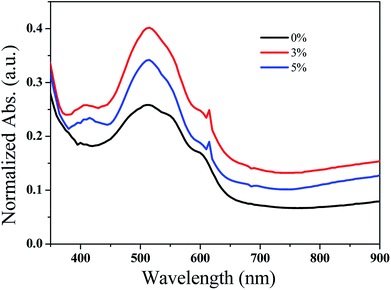
:![[thin space (1/6-em)]](https://www.rsc.org/images/entities/char_2009.gif) 1 and GeQD/NGr nanocomposite at 3 and 5 wt% were prepared in chloroform at 20 mg ml−1 concentration. NGr at 3 wt% was also used in the active layer blend for comparison. The active layer solution was stirred for 4 h at 40 °C. Devices were fabricated in the BHJ architecture of glass/ITO/PEDOT:PSS/P3HT:PCBM:NGr-Ge QDs/LiF/Al as shown in Fig. 1. Indium tin oxide (ITO) coated glass substrates, of 15 Ω/sq sheet resistance, were etched in an acid solution. This was followed by sequential ultrasonication in deionized water, acetone and isopropanol for 10 min each. The substrates were then dried in a vacuum oven at 120 °C for 30 min. Poly(3,4-ethylenedioxythiophene):poly(styrenesulfonate) (PEDOT:PSS) was spin-coated on the substrates at 4500 rpm for 60 s and then dried in the vacuum oven at 120 °C for 20 min. Thereafter, spin coating of the active layer solution was done at 1200 rpm for 30 s on the PEDOT:PSS layer. The samples were then thermally annealed in a tube furnace at 120 °C for 5 min under the flow of nitrogen gas. Eventually, LiF (0.4 nm) and Al electrode (50 nm) were thermally deposited on to the samples under a vacuum at 10−6 mbar base pressure. The current–voltage (J–V) measurements for the devices were done using a Keithley HP2400 source-meter and a solar simulator (model SS50AAA) under air-mass 1.5 global (A.M 1.5G) illumination and integrated power intensity of 100 mW cm−2. The optical absorption spectra of the active layer films were acquired from a Raleigh 1601 UV-vis-NIR spectrophotometer while the films morphology was analysed by SEM. The fabrication and characterization of the devices was carried out in an ambient environment and the effective area for the devices was 4 mm2.
1 and GeQD/NGr nanocomposite at 3 and 5 wt% were prepared in chloroform at 20 mg ml−1 concentration. NGr at 3 wt% was also used in the active layer blend for comparison. The active layer solution was stirred for 4 h at 40 °C. Devices were fabricated in the BHJ architecture of glass/ITO/PEDOT:PSS/P3HT:PCBM:NGr-Ge QDs/LiF/Al as shown in Fig. 1. Indium tin oxide (ITO) coated glass substrates, of 15 Ω/sq sheet resistance, were etched in an acid solution. This was followed by sequential ultrasonication in deionized water, acetone and isopropanol for 10 min each. The substrates were then dried in a vacuum oven at 120 °C for 30 min. Poly(3,4-ethylenedioxythiophene):poly(styrenesulfonate) (PEDOT:PSS) was spin-coated on the substrates at 4500 rpm for 60 s and then dried in the vacuum oven at 120 °C for 20 min. Thereafter, spin coating of the active layer solution was done at 1200 rpm for 30 s on the PEDOT:PSS layer. The samples were then thermally annealed in a tube furnace at 120 °C for 5 min under the flow of nitrogen gas. Eventually, LiF (0.4 nm) and Al electrode (50 nm) were thermally deposited on to the samples under a vacuum at 10−6 mbar base pressure. The current–voltage (J–V) measurements for the devices were done using a Keithley HP2400 source-meter and a solar simulator (model SS50AAA) under air-mass 1.5 global (A.M 1.5G) illumination and integrated power intensity of 100 mW cm−2. The optical absorption spectra of the active layer films were acquired from a Raleigh 1601 UV-vis-NIR spectrophotometer while the films morphology was analysed by SEM. The fabrication and characterization of the devices was carried out in an ambient environment and the effective area for the devices was 4 mm2.
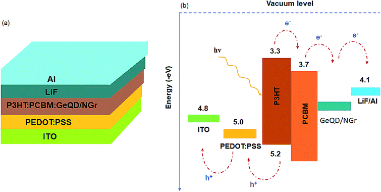 | ||
| Fig. 1 (a) Schematic of the BHJ-SCs with GeQD/NGr nanocomposite in the active layer and (b) energy level diagram of the device materials. | ||
3 Results and discussion
3.1 Germanium quantum dot/nitrogen-doped graphene nanocomposite
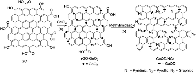
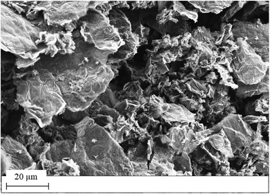
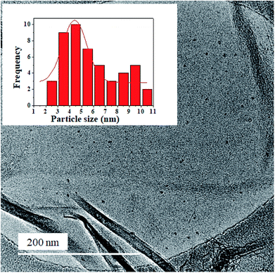
GeQD/NGr nanocomposite was prepared in two subsequent steps as illustrated schematically in Fig. 2. rGO-GeO2 nanocomposite was first synthesized via the microwave-assisted solvothermal reaction using GO as the starting material. Reduction of GO and formation of rGO-GeO2 nanocomposite was simultaneously achieved in this procedure. In the second step, rGO-GeO2 was used as the starting material to prepare GeQD/NGr nanocomposite by thermal treatment. At this stage, N-doping of graphene and formation of the GeQD/NGr nanocomposite were concurrently realized (Fig. 3).The TEM and SEM images of the obtained nanocomposite are shown in Fig. S1† and 3, respectively. Clearly observed from the TEM image are transparent sheets rich in wrinkles and folds with edges characterized by scrolls. The TEM image also shows Ge QDs of uniform distribution attached on the NGr sheets. The surface morphology of the nanocomposite, as observed from the SEM image, is characterized by exfoliated sheets of good lamellar structure; these sheets are also rich in wrinkles. The TEM image of NGr (Fig. S2†) is characterized by folds and scrolls while its SEM image (Fig. S3†) shows aggregated sheets that are rich in wrinkles. Observed from the HR-TEM image of the nanocomposite (Fig. 4), are uniformly distributed Ge QDs anchored on the NGr sheets; these sheets are multi-layered in nature. The size of the Ge QDs is in the range of 2.0–10.6 nm. Inset of Fig. 4 is a histogram that shows the nanoparticles size distribution. A mean diameter of 4.4 nm with a standard deviation of 0.3 nm for the Ge QDs was obtained by performing a Gaussian fit to the histogram. Fig. S4† shows lattice fringes with d-spacing values of 0.34 nm and 0.26 nm. The 0.34 nm d-spacing is typical of NGr while 0.26 nm corresponds to the (201) plane of the diamond phase of cubic Ge. The crystal structure of the nanocomposite as characterized by XRD is illustrated in Fig. S5.† The diffraction peaks at 26°, 47° and 56° are indexed to the (111), (220) and (311) planes of the diamond Ge cubic phase, respectively (JCPDS card no. 04-0545). The XRD pattern of NGr (Fig. S6†) is characterized by a sharp diffraction peak at 26° and a small one at 43°. Thus, in the XRD pattern of the nanocomposite, the NGr peak at 26° overlaps with that of (111) crystal plane of Ge.
Raman spectroscopy was used to evaluate the microstructure of the nanocomposite given its sensitivity to the crystalline state, defects and disorder in carbon-based samples. The Raman spectrum of the GeQD/NGr nanocomposite given in Fig. S7† manifests two peaks at 1355 and 1598 cm−1 corresponding to the D-band and G-band, respectively. The D-band is a signature of defects and disorder in the graphitic structure while the G-band is ascribed to the stretching vibrations of sp2 hybridized carbon atoms. The Raman spectrum of GO is also given in Fig. S7;† the D-band and G-band for GO occurs at 1345 and 1585 cm−1, respectively. Thus, the nanocomposite manifest upward shifts in both the D-and G-bands peak position. A shift in the G-band peak position can be effected by doping,39 defects40 and strains.41 The structural defects include boundaries, vacancies and heteroatoms in the graphitic lattice structure.42 Hence, the observed shift is indicative of charge transfer between the nanocomposite constituents i.e. NGr and Ge. Previous studies on NGr showed downshift of the G-band peak position given the electron-donating capability of N to graphene.6,43 Thus, the upward shift observed for the nanocomposite implies electron transfer from NGr to Ge. The well-documented Tuinstra–Koenig relation,44 ID/IG, which is a ratio of the integrated area of the D-to G-peaks was obtained for the nanocomposite. This ratio is a signature of the crystalline state of carbon-based samples. The nanocomposite exhibited an ID/IG value of 1.19 which is higher than that of GO ca. 0.79. This implies the creation of defects in the graphitic structure upon N and Ge doping of graphene.
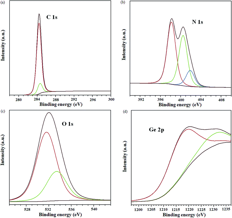
XPS analysis was carried out to evaluate the elemental composition of the nanocomposite, as well as, the respective chemical states. Fig. 5 shows the XPS spectra for the individual elements (C, N, O and Ge) in the nanocomposite. The atomic percentage of C, N, O and Ge was estimated as 95.7, 1.2, 2.6 and 0.5%, respectively. The low doping level of N is attributed to the high reaction temperature which can break some of the C–N bonds.42,45 Curve fitting of the C 1s spectrum (Fig. 5a) mainly yields two peaks at 284.4 and 284.6 eV; these are ascribed to the sp2 hybridized C, implying that the carbon atoms in the nanocomposite are predominantly packed in a honeycomb lattice structure.43,46 Deconvolution of the Ge 2p spectrum yielded two peaks at 1217.4 and 1230.6 eV (Fig. 5d) corresponding to zero-valence Ge (78.2%) and Ge–O bonds (21.8%), respectively. Similarly, two components form the O 1s spectrum (Fig. 5c) i.e. peaks at 531.6 and 533.4 eV, corresponding to the C![[double bond, length as m-dash]](https://www.rsc.org/images/entities/char_e001.gif) O and O
O and O![[double bond, length as m-dash]](https://www.rsc.org/images/entities/char_e001.gif) C–O oxygen functional groups, respectively.42 The N 1s spectrum was deconvoluted to three main peaks at 398.2, 400.5 and 401.9 eV (Fig. 5b) which are assigned to the pyridinic-, pyrrolic- and graphitic-nitrogen, respectively.47,48 Of the different N 1s species in the nanocomposite, the pyridinic-N constituted the highest percentage ca. 43.8% followed by pyrrolic N at 35.4%. The graphitic-nitrogen formed a lower percentage ca. 11.4%. The pyridinic-N results in a local deficiency in electron which implies a high electron affinity49 whereas, the graphitic-N is known to provide delocalized electrons in the graphitic structure which enhances electroconductivity.43 The overall effect of the pyridinic-, pyrrolic- and graphitic-N in the honeycomb structure of graphene is improved electrical conductivity.50 This, taken together with the high electron affinity associated with the pyridinic-N and Ge, favours the use of the nanocomposite in the active layer of OSCs as it would promote charge selectivity and transport.
C–O oxygen functional groups, respectively.42 The N 1s spectrum was deconvoluted to three main peaks at 398.2, 400.5 and 401.9 eV (Fig. 5b) which are assigned to the pyridinic-, pyrrolic- and graphitic-nitrogen, respectively.47,48 Of the different N 1s species in the nanocomposite, the pyridinic-N constituted the highest percentage ca. 43.8% followed by pyrrolic N at 35.4%. The graphitic-nitrogen formed a lower percentage ca. 11.4%. The pyridinic-N results in a local deficiency in electron which implies a high electron affinity49 whereas, the graphitic-N is known to provide delocalized electrons in the graphitic structure which enhances electroconductivity.43 The overall effect of the pyridinic-, pyrrolic- and graphitic-N in the honeycomb structure of graphene is improved electrical conductivity.50 This, taken together with the high electron affinity associated with the pyridinic-N and Ge, favours the use of the nanocomposite in the active layer of OSCs as it would promote charge selectivity and transport.
Thermogravimetric analysis (TGA) was used to determine thermal stability of the nanocomposite; this was carried out in air at a heating rate of 10 °C min−1. The obtained TGA thermogram is given in Fig. S8.† As observed from the thermogram, the nanocomposite manifests good thermal stability up to temperatures as high as 850 °C; this is advantageous for the temperature processing requirements of OSCs. The slight weight increment observed from 250 °C is attributed to the oxidation of Ge to GeO2. A similar trend has been observed for germanium-graphene nanosheets.51
The nitrogen gas absorption–desorption isotherm for the GeQD/NGr nanocomposite is given in Fig. S9.† The observed isotherm is type IV implying that the nanocomposite is a mesoporous material.52 The isotherm is accompanied by a pronounced type H2 hysteresis loop between 0.4–1.0P/Po; this hysteresis is associated with the occurrence of capillary condensation in the mesopores. The pronounced hysteresis is indicative of a high number of mesopores with evenly distributed pore size within the nanocomposite structure.53 A surface area of 67 m2 g−1 was obtained by Brunauer–Emmett–Teller (BET) analysis. This corroborates with the observed SEM image which shows well exfoliated wrinkled sheets. The pore size and volume of the nanocomposite were 15 nm and 0.12 cm3 g−1, respectively.
3.2 Device characterization
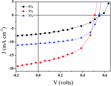 | ||
| Fig. 7 The current–voltage characteristics of the BHJ-SCs with GeQD/NGr in the active layer at different concentrations. | ||
| GeQD/NGr loading (wt%) | Voc (volts) | Jsc (mA cm−2) | FF (%) | PCE (%) | Rs (Ω) |
|---|---|---|---|---|---|
| 0 | 0.56 ± 0.006 | 7.3 ± 0.07 | 45 ± 0.7 | 1.8 ± 0.07 | 363 ± 14 |
| 3 | 0.50 ± 0.008 | 18.9 ± 0.28 | 55 ± 1.8 | 5.1 ± 0.12 | 83 ± 5.6 |
| 5 | 0.56 ± 0.01 | 11.1 ± 0.26 | 54 ± 1.3 | 3.3 ± 0.07 | 382 ± 19 |
A large potential difference between the LUMO of the donor and the acceptor materials promotes charge separation in OSCs. Considering the work function of NGr ca. −4.4 eV (ref. 6) and that of Ge ca. −4.78 eV (ref. 54) in comparison to the LUMO level of P3HT ca. −3.3 eV, a high potential difference is created in the active layer phases for effective exciton dissociation. Thus, geminate charge recombination is minimized in the devices. Moreover, because of the high electron affinity associated with the nanocomposite constituents, its incorporation in the active layer not only offers charge selectivity at the interfaces but also facilitates electrons transfer within the acceptor domains. The charge selectivity of the nanocomposite serves to ensure effective extraction of electrons hence, alleviates the recombination of holes and electrons. Another factor that affects both charge carriers separation and transportation is the nanoscale thin film morphology. Good crystallinity and miscibility of the donor and acceptor materials favours the formation of smooth morphology. Hence, the good crystalline quality of the GeQD/NGr nanocomposite is an additional advantage to its use in the active layer. Therefore, the inlay of GeQD/NGr nanocomposite in the active layer, at optimum concentration, facilitates exciton generation, dissociation and transport of the separated charge carriers to the outside circuitry for enhanced device performance.
 | (1) |
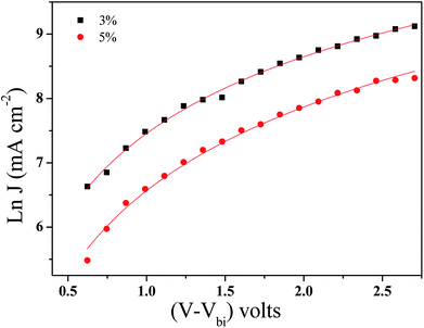 | ||
| Fig. 8 Space charge limited currents of the BHJ-SCs with GeQD/NGr at different concentrations in the active layer; the solid lines are computer fits according to eqn (1). | ||
| GeQD/NGr loading (wt%) | μ0 (cm2 V−1 S−1) | γ (cm V−1) |
|---|---|---|
| 0 | 3.96 × 10⁻⁵ | −1.9 × 10⁻⁴ |
| 3 | 4.81 × 10⁻³ | −1.8 × 10⁻⁴ |
| 5 | 1.53 × 10⁻³ | −8.0 × 10⁻⁴ |
A solar cell with NGr at 3 wt% in the active layer was fabricated and analysed to elucidate the influence of Ge QDs in the photo active layer, on the photovoltaic performance. The obtained J–V plot is shown in Fig. S10.† The device yielded a Voc, Jsc, FF, Rs and PCE of 0.56 V, 10.5 mA cm−2, 50%, 768 Ω and 2.9%, respectively. Relative to the reference device, enhanced performance is achieved with NGr in the active layer, albeit, inferior to that of the GeQD/NGr modified devices. Specifically, the device manifests lower Jsc and higher Rs relative to the nanocomposite modified device implying a relatively higher charge carrier loss. With regards to the enhanced performance relative to the reference device, NGr offers charge selectivity and creates transport pathways for electron transfer hence, suppresses geminate charge recombination; this corroborates with the observation of Jun et al.6 Improved charge transport in the device is elucidated by charge transport analysis (Fig. S11†) which yielded a carrier mobility of 8.09 × 10⁻⁴ μ0 (cm2 V−1 S−1) at a field activation factor of 2.0 × 10⁻⁵ γ (cm V−1); this is an order in magnitude higher than the reference device but lower than the nanocomposite modified devices in the same order. It is therefore evidenced that the incorporation of the Ge QDs in the active layer not only improves the charge selectivity, owing to its high electron affinity, but also adds impetus to the charge transport capability of the active layer blend.
4 Conclusion
In summary, we have demonstrated the influence of GeQD/NGr nanocomposite on the photovoltaic performance of BHJ-SCs. GeQD/NGr nanocomposite was synthesized by microwave-assisted solvothermal reaction followed by thermal treatment. TEM and HR-TEM analysis showed spherical shaped Ge QDs attached on the NGr sheets. Enhanced efficiency was achieved by the inclusion of the nanocomposite in the active layer. The improved PCE originated from enhanced Jsc and FF, giving the devices with nanocomposite in the active layer an edge over the reference device. With the nanocomposite in the active layer, a high electric field is built for effective charge separation. Also, given the high electron affinity of the nanocomposite's constituents, its inclusion in the active layer offers charge selectivity at the interface and aids in electron transfer within the acceptor domains. Charge transport analysis showed increased carrier mobilities for the modified active layer devices. The improved charge transport is attributed to the formation of interconnected pathways upon incorporation of the GeQD/NGr nanocomposite. Because of the additive conductive pathways for charge transfer, non-geminate charge recombination is suppressed in the devices. Therefore, the inclusion of GeQD/NGr nanocomposite in the active layer of BHJ-SCs improves charge carriers generation, separation and transfer to the electrodes to yield an improvement in PCE by up to 183%. The studies presented herein reveal the prospects of tuning the functionality of graphene for optimized performance in PSCs.Conflicts of interest
There are no conflicts to declare.Acknowledgements
The authors are grateful to the National Research Foundation (NRF), the University of KwaZulu-Natal and the UKZN Nanotechnology Platform for supporting this research work. The funding bodies did not participate in the research design, data collection and analysis, manuscript development or in the decision for its submission.References
- B. Kannan, K. Castelino and A. Majumdar, Nano Lett., 2003, 3, 1729–1733 CrossRef.
- M. Sim, J. Shin, C. Shim, M. Kim, S. B. Jo, J.-H. Kim and K. Cho, J. Phys. Chem. C, 2014, 118, 760–766 Search PubMed.
- X. Wan, G. Long, L. Huang and Y. Chen, Adv. Mater., 2011, 23, 5342–5358 CrossRef PubMed.
- W.-Q. Wu, D. Chen, F. Li, A. R. Pascoe, Y.-B. Cheng and R. A. Caruso, Nano Energy, 2017, 32, 187–194 CrossRef.
- N. Gasparini, M. Salvador, T. Heumueller, M. Richter, A. Classen, S. Shrestha, G. J. Matt, S. Holliday, S. Strohm and H. J. Egelhaaf, Adv. Energy Mater., 2017, 22, 1701561 CrossRef.
- G. H. Jun, S. H. Jin, B. Lee, B. H. Kim, W.-S. Chae, S. H. Hong and S. Jeon, Energy Environ. Sci., 2013, 6, 3000–3006 Search PubMed.
- L. Lu, M. A. Kelly, W. You and L. Yu, Nat. Photonics, 2015, 9, 491–500 CrossRef.
- C. Liu, X. Hu, C. Zhong, M. Huang, K. Wang, Z. Zhang, X. Gong, Y. Cao and A. J. Heeger, Nanoscale, 2014, 6, 14297–14304 RSC.
- S. O. Oseni and G. T. Mola, Sol. Energy, 2017, 150, 66–72 CrossRef.
- W.-Q. Wu, D. Chen, Y.-B. Cheng and R. A. Caruso, Sustainable Energy Fuels, 2017, 1, 1960–1967 Search PubMed.
- T. A. Amollo, G. T. Mola, M. Kirui and V. O. Nyamori, Crit. Rev. Solid State Mater. Sci., 2018, 43, 133–157 CrossRef.
- G. S. Selopal, R. Milan, L. Ortolani, V. Morandi, R. Rizzoli, G. Sberveglieri, G. P. Veronese, A. Vomiero and I. Concina, Sol. Energy Mater. Sol. Cells, 2015, 135, 99–105 CrossRef.
- J. Cao, Y. Zhu, X. Yang, Y. Chen, Y. Li, H. Xiao, W. Hou and J. Liu, Sol. Energy Mater. Sol. Cells, 2016, 157, 814–819 CrossRef.
- D. Joly, J.-W. Jung, I.-D. Kim and R. Demadrille, J. Mater. Chem. C, 2016, 4, 10173–10197 RSC.
- H. P. Kim, A. R. bin Mohd Yusoff and J. Jang, Sol. Energy Mater. Sol. Cells, 2013, 110, 87–93 CrossRef.
- R. Sharma, F. Alam, A. Sharma, V. Dutta and S. Dhawan, J. Mater. Chem. C, 2014, 2, 8142–8151 RSC.
- X. Fan, Z. Shen, A. Liu and J.-L. Kuo, Nanoscale, 2012, 4, 2157–2165 RSC.
- W.-Q. Wu, D. Chen, R. A. Caruso and Y.-B. Cheng, J. Mater. Chem. A, 2017, 5, 10092–10109 Search PubMed.
- X. Wang, G. Sun, P. Routh, D.-H. Kim, W. Huang and P. Chen, Chem. Soc. Rev., 2014, 43, 7067–7098 RSC.
- S. U. Lee, R. V. Belosludov, H. Mizuseki and Y. Kawazoe, Small, 2009, 5, 1769–1775 CrossRef PubMed.
- B. Guo, Q. Liu, E. Chen, H. Zhu, L. Fang and J. R. Gong, Nano Lett., 2010, 10, 4975–4980 CrossRef PubMed.
- M. Fan, Z.-Q. Feng, C. Zhu, X. Chen, C. Chen, J. Yang and D. Sun, J. Mater. Sci., 2016, 51, 10323–10349 CrossRef.
- A. J. Marsden, P. Brommer, J. J. Mudd, M. A. Dyson, R. Cook, M. Asensio, J. Avila, A. Levy, J. Sloan and D. Quigley, Nano Res., 2015, 8, 2620–2635 CrossRef.
- B. He, Z. Ren, C. Qi, S. Yan and Z. Wang, J. Mater. Chem. C, 2015, 3, 6172–6177 RSC.
- S. H. Park, J. Chae, M.-H. Cho, J. H. Kim, K.-H. Yoo, S. W. Cho, T. G. Kim and J. W. Kim, J. Mater. Chem. C, 2014, 2, 933–939 RSC.
- H. Wang, T. Maiyalagan and X. Wang, ACS Catal., 2012, 2, 781–794 CrossRef.
- R. Yadav and C. Dixit, Journal of Science: Advanced Materials and Devices, 2017, 2, 141–149 CrossRef.
- Y. Maeda, Phys. Rev. B, 1995, 51, 1658 CrossRef.
- V. I. Klimov, Semiconductor and metal nanocrystals: synthesis and electronic and optical properties, CRC Press, New York, 2003 Search PubMed.
- D. Carolan and H. Doyle, J. Mater. Chem. C, 2014, 2, 3562–3568 RSC.
- J. Fan and P. K. Chu, Small, 2010, 6, 2080–2098 CrossRef PubMed.
- D. D. Vaughn II and R. E. Schaak, Chem. Soc. Rev., 2013, 42, 2861–2879 RSC.
- Y. Kim, N. D. Lam, K. Kim, W.-K. Park and J. Lee, Sci. Rep., 2017, 7, 42693 CrossRef PubMed.
- V. Sorianello, L. Colace, C. Maragliano, D. Fulgoni, L. Nash and G. Assanto, Opt. Mater. Express, 2013, 3, 216–228 CrossRef.
- D. J. Xue, J. J. Wang, Y. Q. Wang, S. Xin, Y. G. Guo and L. J. Wan, Adv. Mater., 2011, 23, 3704–3707 CrossRef PubMed.
- T. A. Amollo, G. T. Mola and V. O. Nyamori, Nanotechnology, 2017, 28, 495703 CrossRef PubMed.
- W. S. Hummers Jr and R. E. Offeman, J. Am. Chem. Soc., 1958, 80, 1339 CrossRef.
- D. Li, K. H. Seng, D. Shi, Z. Chen, H. K. Liu and Z. Guo, J. Mater. Chem. A, 2013, 1, 14115–14121 Search PubMed.
- A. Das, S. Pisana, B. Chakraborty, S. Piscanec, S. Saha, U. Waghmare, K. Novoselov, H. Krishnamurthy, A. Geim and A. Ferrari, Nat. Nanotechnol., 2008, 3, 210–215 CrossRef PubMed.
- A. Das, B. Chakraborty and A. Sood, Bull. Mater. Sci., 2008, 31, 579–584 CrossRef.
- M. Huang, H. Yan, T. F. Heinz and J. Hone, Nano Lett., 2010, 10, 4074–4079 CrossRef PubMed.
- Z. Xing, Z. Ju, Y. Zhao, J. Wan, Y. Zhu, Y. Qiang and Y. Qian, Sci. Rep., 2016, 6, 26146 CrossRef PubMed.
- D. Wei, Y. Liu, Y. Wang, H. Zhang, L. Huang and G. Yu, Nano Lett., 2009, 9, 1752–1758 CrossRef PubMed.
- F. Tuinstra and J. L. Koenig, Chem. Phys., 1970, 53, 1126–1130 Search PubMed.
- A. Śliwak, B. Grzyb, N. Díez and G. Gryglewicz, Appl. Surf. Sci., 2017, 399, 265–271 CrossRef.
- C. Botas, P. Alvarez, C. Blanco, R. Santamaría, M. Granda, M. D. Gutiérrez, F. Rodríguez-Reinoso and R. Menéndez, Carbon, 2013, 52, 476–485 CrossRef.
- S. Kabir, K. Artyushkova, A. Serov, B. Kiefer and P. Atanassov, Surf. Interface Anal., 2016, 48, 293–300 CrossRef.
- J. Pels, F. Kapteijn, J. Moulijn, Q. Zhu and K. Thomas, Carbon, 1995, 33, 1641–1653 CrossRef.
- K. Share, A. P. Cohn, R. Carter, B. Rogers and C. L. Pint, ACS Nano, 2016, 10, 9738–9744 CrossRef PubMed.
- A. Śliwak, N. Díez, E. Miniach and G. Gryglewicz, J. Appl. Electrochem., 2016, 46, 667–677 CrossRef.
- C. Zhong, J.-Z. Wang, X.-W. Gao, D. Wexler and H.-K. Liu, J. Mater. Chem. A, 2013, 1, 10798–10804 Search PubMed.
- K. S. Sing, Pure Appl. Chem., 1985, 57, 603–619 CrossRef.
- Z. Fan, Y. Liu, J. Yan, G. Ning, Q. Wang, T. Wei, L. Zhi and F. Wei, Adv. Energy Mater., 2012, 2, 419–424 CrossRef.
- J. Dillon Jr and H. Farnsworth, J. Appl. Phys., 1957, 28, 174–184 CrossRef.
Footnote |
| † Electronic supplementary information (ESI) available. See DOI: 10.1039/c8ra04223c |
| This journal is © The Royal Society of Chemistry 2018 |

