 Open Access Article
Tunnable rectifying performance of in-plane metal–semiconductor junctions based on passivated zigzag phosphorene nanoribbons
ShaoLong Sua,
Jian Gong*a and
Zhi-Qiang Fan *b
*b
aSchool of Physical Science and Technology, Inner Mongolia University, Hohhot 010021, People's Republic of China. E-mail: ndgong@imu.edu.cn
bSchool of Physics and Electronic Science, Changsha University of Science and Technology, Changsha 410114, People's Republic of China. E-mail: zqfan@csust.edu.cn
First published on 5th September 2018
Abstract
Using first principles density functional theory, we perform a systematic study of the band structures of passivated zigzag phosphorene nanoribbons (ZPNRs) and the transport properties of in-plane metal–semiconductor junctions. It is found that the ZPNR passivated by H, Cl or F atoms is a semiconductor, and the ZPNR passivated by C, O or S atoms is a metal. Therefore, ZPNRs with different passivated atoms can be fabricated into an in-plane metal–semiconductor junction. The calculated current–voltage characteristics indicate that these in-plane metal–semiconductor junctions can exhibit excellent rectification behavior. More importantly, we find that the type of passivated atom plays a very important role in the rectification ratio of this in-plane metal–semiconductor junction. The findings are very useful for the further design of functional nanodevices based on ZPNRs.
1. Introduction
Two-dimensional and monolayered materials have attracted increasing attention day by day and are considered as an alternative to traditional bulk semiconductors for future generation nanodevices due to their intriguing physical properties. Graphene, as a monolayer of hexagonally arranged carbon atoms, is generally believed to be the first two-dimensional material and was deposited by mechanically exfoliating thin sheets from graphite in 2004.1 So far, experimental and theoretical research results show that graphene has extremely high mobility, high thermal conductivity, great electromechanical modulation, and excellent stiffness.2–5 However, the absence of an intrinsic band gap imposes severe challenges on its implementation in logic and memory devices.6 Fortunately, one-dimensional graphene nanoribbons (GNRs) have tunable band gaps depending on different widths, different edge geometrical shapes, and different edge passivated atoms. Consequently, a variety of novel nonlinear electronic transport properties, such as rectification,7–10 negative differential resistance (NDR),11–14 switching,15–18 and spintronic functions have been found in nanodevices based on graphene nanoribbons.19–22Recently, several new two-dimensional materials with puckered honeycomb structures have been found in experiment.23–26 The most prominent among them is phosphorene due to its excellent optical and electronic properties.27–30 Phosphorene has a direct band gap ranging from about 0.3 eV (multilayer phosphorus) to 1.5 eV (mono-layer phosphorene) which makes it have huge potential in applications of transistors.31,32 Like GNRs, one-dimensional phosphorene nanoribbons (PNRs) also have tunable band gaps depending on different widths, different edge geometrical shapes, and different edge passivated atoms. The bare armchair phosphorene nanoribbon (APNR) is a semiconductor with an indirect band gap, and the bare zigzag phosphorene nanoribbon (ZPNR) is a metal.33–35 Through edge hydrogenation, both APNRs and ZPNRs have become semiconductors with a direct band gap.36,37 Besides hydrogen atoms, other passivated atoms also have been proved to play an important role in tuning the band gap of PNRs.38,39 However, the investigations of electronic structure and transport about nanodevices based on PNRs with different passivated atoms are not studied completely yet. In this paper, we perform a detailed analysis of a monolayer contact structure based on zigzag phosphorene nanoribbon with different passivated atoms. We find that a ZPNR passivated by H, Cl or F atoms is semiconductor, and a ZPNR passivated by C, O or S atoms is metal. Therefore, one can use ZPNR with different passivated atoms to fabricate an in-plane metal–semiconductor junction and to achieve the rectify behavior. The calculated results show that the type of passivated atom plays a very important role in the rectification ratio (RR) of this ZPNR in-plane metal–semiconductor junction. Our findings are very useful for the further design of functional nanodevices based on ZPNR.
2. Methods
Band structures of passivated ZPNRs and transport properties of in-plane metal–semiconductor junctions in this work are carried out by using Atomistix ToolKit (ATK) software package, which is based on density-functional theory in combination with the non-equilibrium Green's function.40 The Perdew–Burke–Ernzerhof (PBE) exchange correlation functional and the generalized gradient approximation (GGA) were employed in the first-principle calculation. The real space grid techniques are used with the energy cutoff of 200 Ry in numerical integration. The k-point samplings for calculations of bulk's electronic structures and electronic transport properties of ZPNR in-plane metal–semiconductor junction are 1 × 1 × 21 and 1 × 1 × 100 in the X, Y, and Z directions, respectively. A vacuum buffer space of at least 12 Å is set to avoid spurious interactions. The geometries are optimized until all residual force on each atom is less than 0.01 eV Å−1. When a bias voltage is applied, the current can be calculated by the Landauer formula: .41,42 Here, Vb is the bias voltage, T(E,Vb) is the transmission coefficient, fL(E,Vb) and fR(E,Vb) are the Fermi–Dirac distribution functions of the left and right electrodes.
3. Results and discussions
Geometrical structures and electronic band structures of ZPNRs with different passivated atoms are shown in Fig. 1. The width of ZPNR is 16 in all six unit cells. Previous studies indicated the bare ZPNR is a metal. However, the calculated band structures in Fig. 1(a)–(c) show the bare ZPNRs turns to a semiconductor, when its two edges are passivated by H, F or Cl atoms separately. The conduction band minimum (CBM) and the valence band maximum (VBM) in Fig. 1(a)–(c) all locate at the Γ point, which gives the direct band gap. The direct band gap of H-passivated ZPNR is 1.62 eV which is largest in three models. The direct band gap of Cl-passivated and F-passivated ZPNRs is 1.37 eV and 1.26 eV, respectively. When two edges of the bare ZPNRs are passivated by O, S or C atoms separately, the calculated band structures in Fig. 1(d)–(f) show metallic behavior. For O-passivated ZPNR, there are two bands being past the Fermi level. For S-passivated ZPNR, there are four bands crossing the Fermi level. For C-passivated ZPNR, there are two bands being past the Fermi level directly and another two bands around the Fermi level.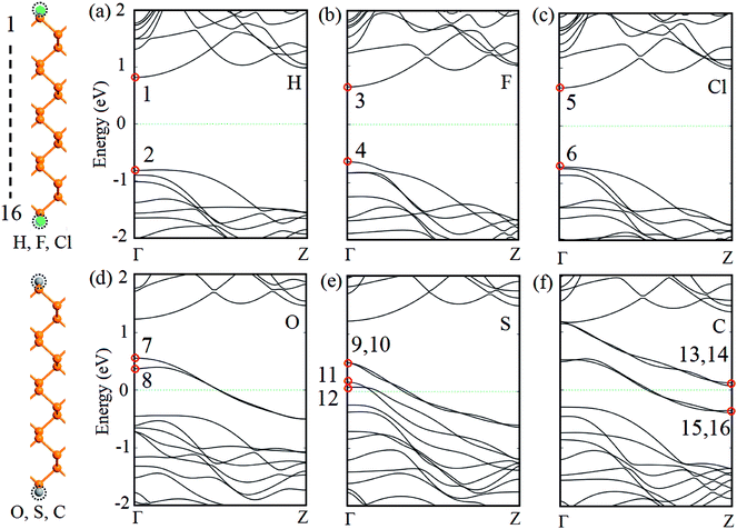 | ||
| Fig. 1 Geometrical structures and electronic band structures of ZPNRs with passivated H, F, Cl, O, S and C atoms, respectively. Fermi level is set to zero. | ||
Besides band structures, the spatial distribution of Bloch states on near-band-edge states also plays an important role in the electronic transport properties of materials. So, the near-band-edge states 1–16 of six passivated ZPNRs (labeled in Fig. 1) were explored and their spatial distributions of Bloch states are shown in Fig. 2. For H-passivated ZPNR, the contours of Bloch state indicate that both CBM (state 1) and VBM (state 2) are contributed by P atoms in the central nanoribbon.37,43 The H atom and its connected P atom are nearly bare in these two states. For F-passivated and Cl-passivated ZPNRs, the contours of Bloch state indicate that both CBM (state 3 or 5) and VBM (state 4 or 6) are contributed by non-edge P atoms and passivated atoms jointly. For O-passivated ZPNR, the contours of Bloch states 7 and 8 are contributed by O atoms and edge P atoms. P atoms in the central nanoribbon have less contribution on the Bloch states. For S-passivated ZPNR, the contours of Bloch states 9 and 10 mainly delocalized on top or down edge S atom, respectively. That means these two bands are mainly induced by S atom. One can see that Bloch states 11 and 12 are contributed by P atoms and S atoms jointly. The spatial distributions of Bloch states in the C-passivated ZPNR are similar to those of S-passivated ZPNR. The Bloch states 13 and 14 mainly delocalized on top or down edge C atom, and the Bloch states 15 and 16 are contributed by edge P atoms and C atoms jointly.
 | ||
| Fig. 2 Spatial distributions of Bloch states corresponding to near-band-edge states 1–16. The isovalues are fixed 0.2 for all Bloch states. | ||
The proposed in-plane metal–semiconductor junction based on different passivated ZPNRs are shown in Fig. 3. We divide the device into three regions: left electrode, right electrode, and central scattering region. The left electrode contains two units of O-passivated or C-passivated ZPNRs, and the right electrode contains two units of H-passivated, F-passivated or Cl-passivated ZPNRs. The central scattering region contains eight units of O-passivated or C-passivated ZPNRs, and eight units of H-passivated, F-passivated or Cl-passivated ZPNRs. For simplicity, the in-plane metal–semiconductor junction based on O-passivated and Cl-passivated ZPNRs is named O–Cl, and other five junctions are named O–H, O–F, C–Cl, C–H and C–F, respectively.
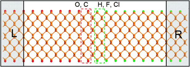 | ||
| Fig. 3 Geometry schematic illustration of the proposed metal–semiconductor junction based on different passivated ZPNRs. The left (L) and right (R) electrodes are indicated by rectangular frames. | ||
The transmission spectra of these six in-plane metal–semiconductor junctions are shown in Fig. 4. In Fig. 4(a), there are large transmission forbidden regions because of the large band gaps of Cl-passivated, H-passivated and F-passivated ZPNRs. The ranges of transmission forbidden regions of O–Cl and O–H junctions are similar to each other. However, the transmission coefficients of the O–H junction around −0.75 eV are smaller than that of the O–Cl junction. It can be explained by the different spatial distributions of Bloch states on the VBM of H-passivated and Cl-passivated ZPNRs. The range of transmission forbidden region of the O–F junction is shorter than other two junctions due to the smaller band gap of F-passivated ZPNR. Although the band gaps of Cl-passivated, H-passivated and F-passivated ZPNRs are different, the right edges of transmission forbidden regions all locate at 1.23 eV for three junctions. In addition, one can find that the ranges of transmission forbidden regions are actually larger than the corresponding band gaps of Cl-passivated, H-passivated and F-passivated ZPNRs. In Fig. 4(b), the transmission spectra are similar to that of Fig. 4(a). The range of the transmission forbidden region in the C–F junction is shorter than other two junctions. However, the right edge of transmission forbidden regions all locate at 0.97 eV for C–Cl, C–H and C–F junctions. Therefore, the ranges of the transmission forbidden regions in Fig. 4(b) are shorter than that of Fig. 4(a).
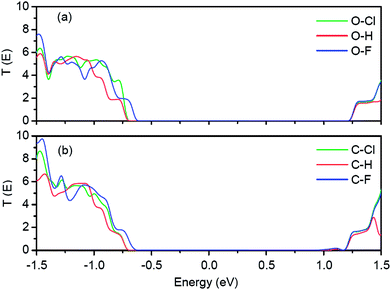 | ||
| Fig. 4 (a) Transmission spectra of O–Cl, O–H and O–F junctions. (b) Transmission spectra of C–Cl, C–H and C–F junctions. Fermi energy is set to zero in the energy scale. | ||
To explain the right edges of transmission forbidden regions all locating at the same energy in Fig. 4(a), we plot the projected density of states of the left electrode and the right electrode for O–Cl, O–H and O–F junctions in Fig. 5. Here, L–O indicates projected density of states of the left O-passivated ZPNR and R–Cl, R–H and R–F indicate projected density of states of the right Cl-passivated, H-passivated and F-passivated ZPNRs, respectively. In Fig. 5(a), one can find that a forbidden region exists in the projected density of states of the right Cl-passivated ZPNR. The range of this forbidden region is equal to the band gap of the Cl-passivated ZPNR. For the left O-passivated ZPNR, a series of peaks spread around Fermi energy. But, there still exists a forbidden region from 0.56 eV to 1.23 eV, which is in agreement with band structure of the O-passivated ZPNR in Fig. 1(d). As a result, the right edge of transmission forbidden region of the O–Cl junction locates at 1.23 eV and the range of transmission forbidden region is actually larger than the corresponding band gap of the Cl-passivated ZPNR. When the passivated atoms of right ZPNR change from Cl atom to H or F atoms, the projected density of state of the left O-passivated ZPNR in Fig. 5(b) or (c) is nearly same to that in Fig. 5(a). Consequently, the right edge of transmission forbidden region of the O–H junction or the O–F junction also locate at 1.23 eV.
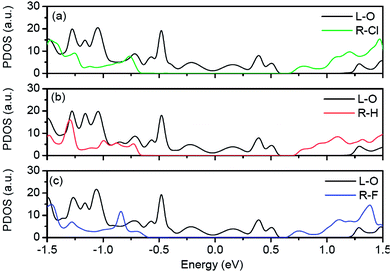 | ||
| Fig. 5 Projected density of states of left electrode and right electrode for O–Cl, O–H and O–F junctions, respectively. Fermi energy is set to zero in the energy scale. | ||
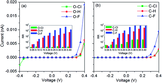
The current–voltage characteristics of six in-plane metal–semiconductor junctions are illustrated in Fig. 6. In Fig. 6(a), one can find the currents of O–H and O–F junctions are always small in the negative bias region. However, the currents of these two junctions will increase rapidly after 0.25 V. So, the current–voltage curves in the whole bias region are asymmetrical and show the rectification performances. For the O–Cl junction, the current–voltage curve is also asymmetrical. But, the rectification performance is not intensive because its currents are also big after −0.3 V. In general, the rectification performance can be evaluated by the rectification ratio which is the ratio of the positive bias current to the negative bias one, RR (V) = I (+V)/I(−V). For the O–F junction, RR will increase gradually with the bias, and the maximal RR nearly approximates 104 at 0.35 V. The average RR of the O–H junction is smaller than that of the O–F junction. The maximal RR can approximate 103 at 0.4 V. The average RR of the O–Cl junction is very small because of its large current at negative bias region. In Fig. 6(b), one can find that currents of C–Cl, C–H and C–F junctions are always very small in the negative bias region. However, currents of the C–F junction will increase rapidly after 0.25 V and the currents of C–Cl and C–H junctions will increase rapidly after 0.3 V. Consequently, current–voltage characteristics of these three junctions also show the rectification performances. The average RR of C–F junction is also largest in three junctions. In addition, the RRs of C–Cl, C–H and C–F junctions are all larger than those of O–Cl, O–H and O–F junctions, respectively. Therefore, one can conclude that the types of the passivated atoms play an important role on the rectification performances of these in-plane metal–semiconductor junctions.
To reveal the origins of the different rectification performances in Fig. 6, we plot the transmission spectra of C–Cl and C–F junctions at several representative bias voltages in Fig. 7. As we describing in the method, the current of the junctions is calculated by the Landauer formula:  . Here, Vb is the bias voltage, T(E,Vb) is the transmission coefficient. When two junctions are applied on the positive bias, the potential of left electrode is raised and the potential of right electrode is reduced. So, the band gap of right Cl-passivated or F-passivated ZPNR shifts to right relative to Fermi energy (left C-passivated ZPNR). As a result, the transmission spectra would shift to right gradually and the left edges of the transmission forbidden regions get close to Fermi energy. So, the total transmission coefficients in the bias window increase gradually leading to the increasing of the current. However, in negative bias region, the potential of left electrode is reduced and the potential of right electrode is raised. So, the transmission spectra would shift to left with increasing of negative bias. The left edges of the transmission forbidden regions get far away from Fermi energy. Changes of total transmission coefficients in the bias window are quite inconspicuous resulting in the small current. As a result, current–voltage characteristics of two junctions show the rectification performances. Because the F-passivated ZPNR has a smaller band gap than the Cl-passivated ZPNR, the left edge of the transmission forbidden region of the C–F junction is closer to Fermi energy than that of the C–Cl junction. At the same positive bias, the current of the C–F junction is larger than that of C–Cl junction. That's why we can find that the rectification performance of the C–F junction is more intensive than that of the C–Cl junction.
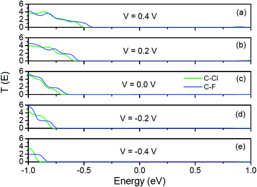 | ||
| Fig. 7 Transmission spectra of C–Cl and C–F junctions at several representative bias voltages. Fermi energy is set to zero in the energy scale. | ||
4. Conclusion
In summary, we have investigated the band structures of passivated ZPNRs and transport properties of in-plane metal–semiconductor junctions by using density-functional theory in combination with the non-equilibrium Green's function. Our study shows that the ZPNR passivated by H, Cl or F atoms is a semiconductor, and the ZPNR passivated by C, O or S atoms is a metal. Then, we use ZPNRs with different passivated atoms to fabricate an in-plane metal–semiconductor junction. The calculated current–voltage characteristics indicate that these in-plane metal–semiconductor junctions can exhibit excellent rectification behavior. More importantly, we find that the type of passivated atom plays a very important role in the rectification ratio (RR) of this in-plane metal–semiconductor junction. The maximal RR of O–F and C–F junctions nearly approximates 104. The findings are very useful for the further design of functional nanodevices based on ZPNR.Conflicts of interest
There are no conflicts to declare.Acknowledgements
This work was supported by the National Natural Science Foundation of China (Grant No. 11464032 and 11674039). One of authors Zhi-Qiang Fan also express his thanks for the Scientific Research Fund of Hunan Provincial Education Department (Grant No. 15A004).References
- K. S. Novoselov, A. K. Geim, S. V. Morozov, D. Jiang, Y. Zhang, S. V. Dubonos, I. V. Grigorieva and A. A. Firsov, Science, 2004, 306, 666 CrossRef PubMed.
- E. H. Hwang, S. Adam and S. D. Sarma, Phys. Rev. Lett., 2007, 98, 186806 CrossRef PubMed.
- S. Ghosh, I. Calizo, D. Teweldebrhan, E. P. Pokatilov, D. L. Nika, A. A. Balandin, W. Bao, F. Miao and C. N. Lau, Appl. Phys. Lett., 2008, 92, 151911 CrossRef.
- J. S. Bunch, A. M. van der Zande, S. S. Verbridge, I. W. Frank, D. M. Tanenbaum, J. M. Parpia, H. G. Craighead and P. L. McEuen, Science, 2008, 315, 490 CrossRef PubMed.
- X. J. Wu and X. C. Zeng, Nano Lett., 2009, 9, 250 CrossRef PubMed.
- F. Schwierz, Nat. Nanotechnol., 2010, 5, 487 CrossRef PubMed.
- M. G. Zeng, L. Shen, M. Yang, C. Zhang and Y. P. Feng, Appl. Phys. Lett., 2011, 98, 053101 CrossRef.
- J. Li, Z. H. Zhang, G. Kwong, W. Tian, Z. Q. Fan and X. Q. Deng, Carbon, 2013, 61, 284 CrossRef.
- H. Q. Wan, B. H. Zhou, W. H. Liao and G. H. Zhou, J. Chem. Phys., 2013, 138, 034705 CrossRef PubMed.
- D. Zhang, M. Q. Long, X. J. Zhang, J. Ouyang and H. Xu, J. Appl. Phys., 2017, 121, 093903 CrossRef.
- Z. Y. Li, H. Y. Qian, J. Wu, B. L. Gu and W. H. Duan, Phys. Rev. Lett., 2008, 100, 206802 CrossRef PubMed.
- K. M. M. Habib and R. K. Lake, Phys. Rev. B, 2012, 86, 045418 CrossRef.
- S. L. Yan, M. Q. Long, X. J. Zhang and H. Xu, Phys. Lett. A, 2014, 378, 960 CrossRef.
- J. Liu, Z. H. Zhang, X. Q. Deng, Z. Q. Fan and G. P. Tang, Org. Electron., 2015, 18, 135 CrossRef.
- X. R. Wang, X. L. Li, L. Zhang, Y. K. Yoon, P. K. Weber, H. L. Wang, J. Guo and H. J. Dai, Science, 2009, 324, 768 CrossRef PubMed.
- H. Q. Wan, B. H. Zhou, X. W. Chen, C. Q. Sun and G. H. Zhou, J. Phys. Chem. C, 2012, 116, 2570 CrossRef.
- Z. Q. Fan and K. Q. Chen, Sci. Rep., 2014, 4, 5976 CrossRef PubMed.
- Z. Q. Fan, Z. H. Zhang, F. Xie, X. Q. Deng, G. P. Tang, C. H. Yang and K. Q. Chen, Org. Electron., 2015, 18, 101 CrossRef.
- D. Wang, Z. H. Zhang, Z. Zhu and B. Liang, Sci. Rep., 2014, 4, 7587 CrossRef PubMed.
- Z. Q. Fan, F. Xie, X. W. Jiang, Z. M. Wei and S. S. Li, Carbon, 2016, 98, 179 CrossRef.
- L. L. Cui, M. Q. Long, X. J. Zhang, X. M. Li, D. Zhang and B. C. Yang, Phys. Lett. A, 2016, 380, 730 CrossRef.
- Z. Q. Fan, W. Y. Sun, Z. H. Zhang, X. Q. Deng, G. P. Tang and H. Q. Xie, Carbon, 2017, 122, 687 CrossRef.
- N. Lu, H. Y. Guo, L. Li, J. Dai, L. Wang, W. N. Mei, X. J. Wu and X. C. Zeng, Nanoscale, 2014, 6, 2879 RSC.
- B. Zhu, X. J. Zhang, B. W. Zeng, M. J. Li and M. Q. Long, Org. Electron., 2017, 49, 45 CrossRef.
- Z. Q. Fan, X. W. Jiang, J. W. Luo, L. Y. Jiao, R. Huang, S. S. Li and L. W. Wang, Phys. Rev. B, 2017, 96, 165402 CrossRef.
- Z. Q. Fan, X. W. Jiang, J. Z. Chen and J. W. Luo, ACS Appl. Mater. Interfaces, 2018, 10, 19271 CrossRef PubMed.
- L. Li, Y. Yu, G. J. Ye, Q. Ge, X. Ou, H. Wu, D. Feng, X. H. Chen and Y. Zhang, Nat. Nanotechnol., 2014, 9, 372 CrossRef PubMed.
- Q. Wei and X. Peng, Appl. Phys. Lett., 2014, 104, 251915 CrossRef.
- X. L. Li, L. Ma, D. Y. Wang, X. C. Zeng, X. J. Wu and J. L. Yang, Nanoscale, 2016, 8, 17801 RSC.
- Y. Jing, X. Zhang and Z. Zhou, Wiley Interdiscip. Rev.: Comput. Mol. Sci., 2016, 6, 5 Search PubMed.
- A. S. Rodin, A. Carvalho and A. H. C. Neto, Phys. Rev. Lett., 2014, 112, 176801 CrossRef PubMed.
- S. Das, W. Zhang, M. Demarteau, A. Hoffmann, M. Dubey and A. K. Roelofs, Nano Lett., 2014, 14, 5733 CrossRef PubMed.
- H. Y. Guo, N. Lu, J. Dai, X. J. Wu and X. C. Zeng, J. Phys. Chem. C, 2014, 118, 14051 CrossRef.
- W. F. Li, G. Zhang and Y. W. Zhang, J. Phys. Chem. C, 2014, 118, 22368 CrossRef.
- A. Carvalho, A. S. Rodin and A. H. Castro Neto, Europhys. Lett., 2014, 108, 47005 CrossRef.
- V. Tran and L. Yang, Phys. Rev. B, 2014, 89, 245407 CrossRef.
- Q. Y. Wu, L. Shen, M. Yang, Y. Q. Cai, Z. G. Huang and Y. P. Feng, Phys. Rev. B, 2015, 92, 035436 CrossRef.
- X. H. Peng, A. Copple and Q. Wei, J. Appl. Phys., 2014, 116, 144301 CrossRef.
- N. Chen, Y. P. Wang, Y. W. Mu, Y. F. Fan and S. D. Li, Phys. Chem. Chem. Phys., 2017, 19, 25441 RSC.
- M. Brandbyge, J. L. Mozos, P. Ordejón, J. Taylor and K. Stokbro, Phys. Rev. B, 2002, 65, 165401 CrossRef.
- M. Büttiker, Y. Imry, R. Landauer and S. Pinhas, Phys. Rev. B, 1985, 31, 6207 CrossRef.
- Z. Q. Fan, K. Q. Chen, Q. Wan, B. S. Zhou, W. H. Duan and Z. Shuai, Appl. Phys. Lett., 2008, 92, 263304 CrossRef.
- Z. Q. Fan, W. Y. Sun, X. W. Jiang, J. W. Luo and S. S. Li, Org. Electron., 2017, 44, 20 CrossRef.
| This journal is © The Royal Society of Chemistry 2018 |

