 Open Access Article
Two-dimensional topological insulators of Pb/Sb honeycombs on a Ge(111) semiconductor surface
Xingkai Hu ,
Zhaoxia Pang,
Xinlian Chen,
Miaojuan Ren and
Ping Li*
School of Physics and Technology, University of Jinan, Jinan, Shandong, China 250022. E-mail: ss_lip@ujn.edu.cn
First published on 12th October 2018
Abstract
Based on first-principles hybrid functional calculations, we demonstrate the formation of two-dimensional (2D) topological insulators (TIs) of Pb/Sb honeycombs on Ge(111) semiconductor surface. We show that 1/3 Cl-covered Ge(111) surface offers an ideal template for metal deposition. When Pb and Sb atoms are deposited on Cl–Ge(111) surface, they spontaneously form a hexagonal lattice (Pb/Sb@Cl–Ge(111)). The Pb/Sb@Cl–Ge(111) exhibits a 2D TI state with large bulk gap of 0.27 eV for Pb@Cl–Ge(111) and 0.81 eV for Sb@Cl–Ge(111). The mechanism of 2D TI state is the substrate orbital-filtering effect that effectively removes the pz bands of Pb(Sb) away from the Fermi level, leaving behind only the px and py orbitals at the Fermi level. Our findings pave another way for future design of 2D topological insulators on conventional semiconductor surface, which promotes the application of 2D TIs in spintronics and quantum computing devices at room-temperature.
I Introduction
In the last decade, two-dimensional (2D) topological insulators (TIs), known as quantum spin hall insulators (QSHs), have attracted considerable attention.1–3 2D TIs exhibit novel electronic properties with topologically protected helical metallic surface or spin-polarized gapless edge states while maintaining an insulating bulk gap, and offer an exciting new realm of electronic/spintronic applications and quantum computing devices4,5 in the future. Recently, some studies have largely enriched the family of 2D TIs, beyond graphene.6,7 The predicted 2D TIs include Bi/Sb films,8,9 Sn films,10 silicene/germanene,11,12 SiTe films,13 transition metal dichalcogenides14 and 2D organometallic frameworks.15,16 Usually, these 2D TIs are considered in a free-standing form to support their exotic electronic properties. However, the free-standing 2D TIs often need to be transferred to a substrate for measurement or for making a device. When these freestanding films are placed on a foreign substrate, the interaction between the films and the substrates can change the electronic structures and topological properties of the films. Some experimental studies have grown bismuth17 on various substrates, and pointed out that the freestanding films' properties are expected to be influenced by the underlying substrate in real applications.18 So, the interaction between films and substrates need more study on theoretically. In addition to, 2D TIs grown on a substrate or formed as an interface are so far limited to quantum well systems19,20 with small bands gap, and do not exhibit quantum spin Hall (QSH) state at room temperature. These considerations make it clear that there is great need to search for new 2D TI systems, which not only host large band gaps, but also maintain their topological properties on suitable semiconducting substrates at room temperature.Recently, it has been theoretically proposed that 2D TIs can effectively form on a semiconductor substrate,21,22 where 2D overlayers are atomically bonded to the underlying substrate and have QSH state at room temperature. Studies show that it is the substrate that stabilizes the overlayer, and makes the overlayer to generate the QSH state by acting as an orbital filter to critically select the orbital composition around the Fermi level.
2D TIs maintaining their topological properties at room temperature must have large band gap. One approach increasing the band gaps of TIs is to use heavy elements with the strong spin orbit coupling (SOC) effects. At present, group IV (Si, Ge, Sn, Pb) and group V (As, Sb, Bi) with chemical functionalization have been demonstrated to possess topological properties.23–27 However, these 2D TIs are in a free-standing form. There are few studies on the effects of Pb and Sb on substrates. Specifically, in 2017, bismuthene with 0.8 eV band gap has been successfully prepared on the SiC(0001) surface by J. Schäfer in experiment using molecular beam epitaxy.22 This study motivate us to think that the preparation of Pb and Sb on Ge(111) surface may be possible and Pb and Sb at Ge(111) surface may be topological insulators.
In this study, we devise the model of Pb(Sb) honeycombs on a 1/3 Cl-covered Ge(111) surface, and employed first-principles calculations to study the interaction between Pb(Sb) overlayers and Ge(111) substrates. Our studies show that a 1/3 Cl-covered Ge(111) surface offers an ideal template for metal deposition, which spontaneously forms a hexagonal lattice with high thermodynamic stability, and Pb(Sb) on Ge(111) surface exhibit a 2D TI state with a large band gap of 0.27 eV for Pb on Ge(111) and 0.81 eV for Sb on Ge(111). In order to verify topological properties of the structures, we investigate the electronic structures of Pb(Sb) on a Ge(111) surface. Research results show that Ge(111) substrate act as an orbital filter to critically select the orbital composition around the Fermi level, leading to Pb and Sb overlayers become topological insulators. Our results point out another route, by choosing appropriate overlayer and substrate, to generate and protect the topological phase of heavy elements.
II Methods
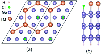
The six layers of √3 × √3 phase semiconductor Ge(111) surface was structured. The dangling bonds of the bottom structure are passivated by H to avoid surface reconstruction. The top surface of the structure is firstly covered by 1/3 Cl forming into patterned Ge(111) surface. When 2/3 TM (Sb and Pb) deposite on a Cl–Ge(111) surface, they will self-assemble into a hexagonal lattice, as shown in Fig. 1.We have performed the first-principles density functional theory (DFT) to calculate the band structures of 2D hexagonal lattices of Sb and Pb atoms grown on a patterned Cl-saturated Ge(111) surface (metal@Cl–Ge). In order to compare with the band structures by standard DFT, we perform a hybrid function, Heyd-Scuseria-Ernzerhof (HSE),28 as implemented in the Vienna Ab-initio Simulation Package(VASP),29 to investigate the electronic structures of metal@Cl–Ge. The kinetic cutoff energy is set at 400 eV. Brillouin-zone integration is carried out at a 9 × 9 × 1 K-grid. The symmetry unrestricted optimizations for geometry are performed using the conjugate gradient scheme until the maximum force is smaller than 0.02 eV Å−1. The self-consistency criteria for electronic structure calculations, with or without spin–orbit coupling (SOC), are sat at 10−6 eV. The vacuum of at least 20 Å is included in the Z direction to avoid the interaction between layers.
III Results and discussion
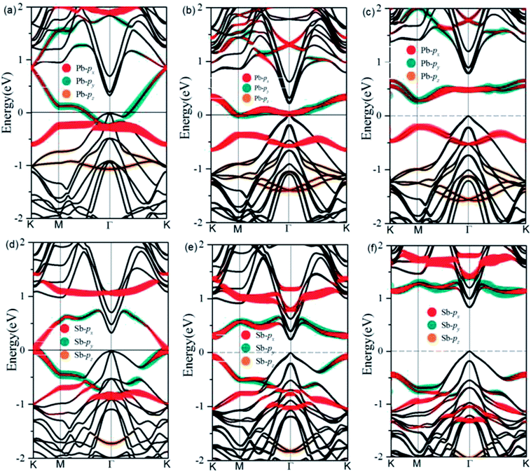
After optimization, we find a very strong binding between the deposited metal atoms and the exposed Ge atoms in the Cl–Ge(111) surface, as evidenced by the calculated adsorption length of 2.79 Å and 2.62 Å for Pb@Cl–Ge(111) and Sb@Cl–Ge(111), respectively. The high structural stability is verified by the formation energy defined as Ead = [EM@Cl–Ge(111) − 2EM − ECl–Ge(111)]/2, where EM@Cl–Ge(111) denotes the energy of metal @ Ge(111) surfaces, EM denotes the energy of a single metal atom, and ECl–Ge(111) denotes the energy of a Cl–Ge(111) surface without metal. The adsorption energies are found to be 2.94 eV, 2.57 eV for Pb, Sb, respectively, indicating the high thermodynamic stability of the systems.To examine the band topology of metal@Cl–Ge(111) surface, the band structures are discussed without SOC and with SOC by the standard DFT method, and with SOC by HSE, as shown in Fig. 2. For Pb@Cl–Ge(111) surface, in the absence of SOC (Fig. 2(a)), we can see there are two Dirac bands residing inside the bulk gap of Ge with a Dirac point at point K, which locates ∼0.85 eV above the Fermi level. Analysis of band composition further show that the two Dirac bands consist of px and py orbitals of Pb atoms, and the upper Dirac band overlaps with the conduction bands of Ge. When the effect of SOC is taken into consideration (Fig. 2(b)), we find that two Dirac bands are split apart by SOC, and the upper branch of Dirac bands moving completely into the Ge conduction bands with one energy gap of ∼0.41 eV at K point. The energy of the lower branch of Dirac bands at K point is higher than the energy of Ge conduction bands minimum at Γ point. The Fermi level is through the lower branch of Dirac bands, so the Pb@Cl–Ge(111) is clearly a metal. Because the standard DFT is known to underestimate band gap, we used a hybrid functional (HSE) to calculate the band structure of metal @Cl–Ge(111) again, shown in Fig. 2(c) and (f). Comparing the band structures using the standard DFT method (shown in Fig. 2(b)), one sees that the bulk band gap of Ge is larger, which is about 0.81 eV at Γ point, being in a very good agreement with the experimental value 0.8 eV. The lower branch of Dirac bands of Pb is still inside the bulk gap of Ge, 0.27 eV lower than Ge conduction bands minimum at Г point.
For Sb@Cl–Ge(111) surface, the band structures without SOC and with SOC are shown in Fig. 2(d)–(f). There are two Dirac bands residing inside the bulk gap of Ge and a Dirac point at K point, which locates nearby the Fermi level without SOC. Over against the band structures without SOC, SOC induces two Dirac bands to split apart. The energy gap is about 0.32 eV at point K, and the global gap is 0.23 eV at Г point. When we calculate the band structures by HSE, the energy gap is about 1.56 eV at point K, and the global gap is 0.81 eV at Г point.
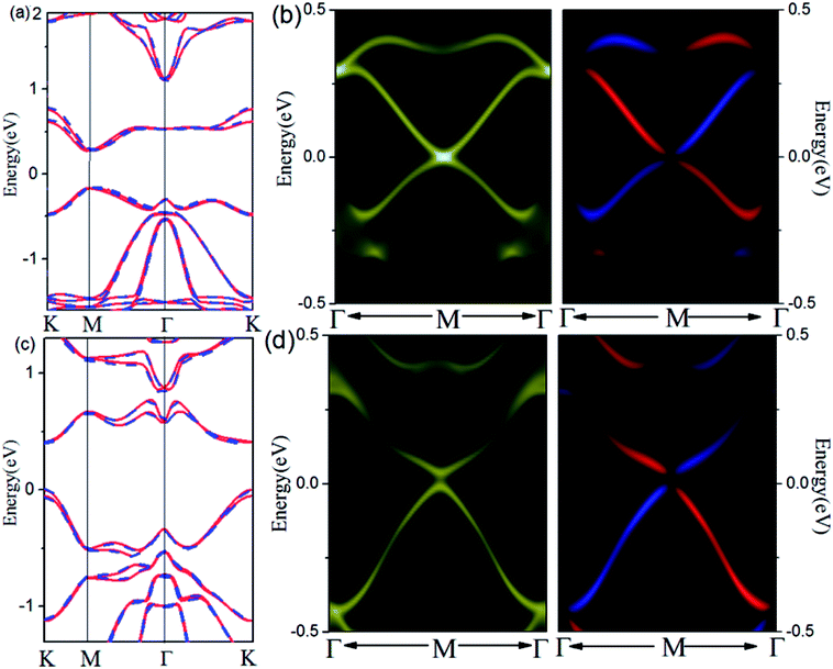
The SOC-induced gap opening at Dirac point indicates that Pb and Sb @Cl–Ge(111) may be a promising 2D TI material for practical applications in electronics and spintronics. To check this, we calculate the topological edge state by the Wannier90 package,30 as shown in Fig. 3. Using DFT bands as input, we construct Hamiltonian with these functions. Fig. 3(a) (for Pb) and Fig. 3(c) (for Sb) show the fitting of tight-binding band structures around the Fermi level using the Wannier90 package to the HSE band structures for Pb@Cl–Ge(111) and the standard DFT band structures for Sb@Cl–Ge(111), which is in a very good agreement. Then the edge Green's functions31,32 of a semi-infinite Pb (Sb) @Cl–Ge(111) are constructed, as shown in Fig. 3(b) and (d). From Fig. 3(b) and (d), we can see the gapless edge states that connect the upper and lower band edge of the bulk gap, forming a 1D Dirac cone at point M. Besides, the counter-propagating edge states exhibit opposite spin polarizations, in accordance with the spin-momentum locking of 1D helical electron. These indicate that the Pb (Sb) @Cl–Ge(111) is 2D TIs with a band gap of 0.27 eV for Pb @Cl–Ge(111) and 0.81 eV for Sb @Cl–Ge(111).
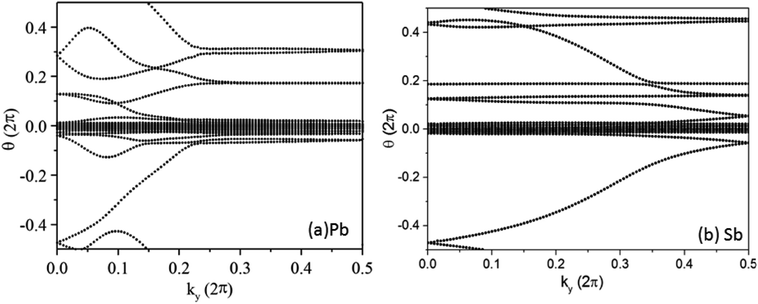
In the Pb/Sb@Cl–Ge(111), as the spatial inversion symmetry is absent, we can calculate topological Z2 invariant by Wilson loop methods base on the U(2N) non-Abelian Berry connection by Yu et al.33 to prove the system is a promising 2D TI. In this method, each state of nth occupied band is indexed by |n,kx,ky〉, and a square matrix F(kx,ky) containing the overlap integrals [F(kx,ky)]mn = 〈|m,kx,i,ky|kx,i+1,ky〉 is defined. The complex unitary square matrix is calculated by  Complex eigenvalues λ(ky) have phase angle θ. Here
  is the discrete spacing of Nx points along kx direction. The Z2 invariant can be obtained by counting the even or odd number of crossings of any arbitrary horizontal reference line. The calculated Wannier function centers evolution of Pb/Sb@Cl–Ge(111) is shown in Fig. 4. It can be seen that the Wannier function centers evolution curves cross any arbitrary reference lines odd times, thus indicating Z2 = 1.
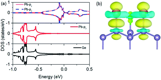
To understand the physical mechanism of 2D TI states, we analyzed the partial density of states (DOS) around the Fermi level and the charge density redistribution induced by Pb atom surface adsorption for Pb@Cl–Ge(111) system, as shown in Fig. 5. From Fig. 5(a), we can see that the Dirac bands mainly consist of px and py orbitals of Pb, with little contribution from the pz orbital of Pb and Ge orbitals. The pz orbital of Pb hybridizes strongly with the sp3 dangling bond of the exposed surface Ge atom overlapping in the same energy range. From the charge density redistribution (shown in Fig. 5(b)), it clearly shows charge redistribution induced by Ge surface mainly happens to the pz orbital of Pb. This is substrate orbital-filtering mechanism proposed by Zhou21 that the Ge substrate effectively removes the pz bands of Pb, leaving behind only the px and py orbitals at the Fermi level. This mechanism is the key to producing 2D TI states according to a four-band model of topological phase in a hexagonal lattice.34
IV Conclusion
Based on hybrid function HSE calculations, we predict substrate supported two quantum spin Hall insulators with extraordinarily large bulk gap of 0.27 eV for Pb@Cl–Ge(111) and 0.81 eV for Sb@Cl–Ge(111). The intrinsic QSH states in Pb(Sb)@Cl–Ge(111) are determined by Z2 invariant and the presence of helical edge states. The substrate orbital-filtering mechanism could be used to understand the mechanism of topological properties of Pb(Sb)@Cl–Ge(111). Our results point out a new materials platforms (TM @Cl–Ge(111)) to protect the topological phase of heavy elements at room-temperature in spintronic applications.Conflicts of interest
There are no conflicts to declare.Acknowledgements
This work was supported by the National Natural Science Foundation of China (Grant No. 11304121), the Natural Science Foundation of Shandong Province (Grant No. ZR2018QA006, ZR2017MA047), Research Fund for the Doctoral Program of University of Jinan (Grant No. XBS1703).References
- M. Z. Hasan and C. L. Kane, Rev. Mod. Phys., 2010, 82, 3045–3067 CrossRef CAS.
- X. L. Qi and S. C. Zhang, Rev. Mod. Phys., 2010, 83, 175–179 Search PubMed.
- L. Kou, Y. Ma, Z. Sun, T. Heine and C. Chen, J. Phys. Chem. Lett., 2017, 8, 1905–1919 CrossRef CAS PubMed.
- C. Xu and J. E. Moore, Phys. Rev. B: Condens. Matter Mater. Phys., 2006, 73, 045322 CrossRef.
- B. A. Bernevig, T. L. Hughes and S. c. Zhang, science, 2006, 314, 1757 CrossRef CAS PubMed.
- C. L. Kane and E. J. Mele, Phys. Rev. Lett., 2005, 95, 226801 CrossRef CAS PubMed.
- C. L. Kane and E. J. Mele, Phys. Rev. Lett., 2005, 95, 146802 CrossRef CAS PubMed.
- M. Wada, S. Murakami, F. Freimuth and G. Bihlmayer, Phys. Rev. B: Condens. Matter Mater. Phys., 2010, 83, 812–819 Search PubMed.
- P. F. Zhang, Z. Liu, W. Duan, F. Liu and J. Wu, Phys. Rev. B: Condens. Matter Mater. Phys., 2012, 85, 151–152 Search PubMed.
- Y. Xu, B. Yan and H.-J. Zhang, et al., Phys. Rev. Lett., 2013, 111, 136804 CrossRef PubMed.
- C.-C. Liu, W. Feng and Y. Yao, Phys. Rev. Lett., 2011, 107, 076802 CrossRef PubMed.
- L. Kou, Y. Ma, B. Yan, X. Tan, C. Chen and S. C. Smith, ACS Appl. Mater. Interfaces, 2015, 7, 19226 CrossRef CAS PubMed.
- Y. Ma, L. Kou, Y. Dai and T. Heine, Phys. Rev. B, 2016, 94, 201104 CrossRef.
- Y. Ma, L. Kou, X. Li, Y. Dai and T. Heine, Phys. Rev. B: Condens. Matter Mater. Phys., 2015, 93, 235451 CrossRef.
- Z. F. Wang, Z. Liu and F. Liu, Nat. Commun., 2015, 4, 1471 CrossRef PubMed.
- L. Zheng, Z. F. Wang, J. W. Mei, Y. S. Wu and L. Feng, Phys. Rev. Lett., 2012, 110, 793–799 Search PubMed.
- C. Sabater, D. Gosálbezmartínez, J. Fernándezrossier, J. G. Rodrigo, C. Untiedt and J. J. Palacios, Phys. Rev. Lett., 2013, 110, 1–10 CrossRef PubMed.
- T. Hirahara, N. Fukui and T. Shirasawa, et al., Phys. Rev. Lett., 2012, 109, 227401 CrossRef CAS PubMed.
- A. Roth, C. Brüne, H. Buhmann, L. W. Molenkamp, J. Maciejko, X. L. Qi and S. C. Zhang, Science, 2009, 325, 294–297 CrossRef CAS PubMed.
- I. Knez, R. R. Du and G. Sullivan, Phys. Rev. Lett., 2011, 107, 136603 CrossRef PubMed.
- M. Zhou, W. Ming, Z. Liu, Z. Wang, P. Li and F. Liu, Proc. Natl. Acad. Sci. U. S. A., 2014, 111, 14378–14381 CrossRef CAS PubMed.
- F. Reis, G. Li, L. Dudy, M. Bauernfeind, S. Glass, W. Hanke, R. Thomale, J. Schäfer and R. Claessen, Science, 2017, 357, 287–290 CrossRef CAS PubMed.
- Z. Song, C. C. Liu, J. Yang, J. Han, M. Ye, B. Fu, Y. Yang, Q. Niu, J. Lu and Y. Yao, NPG Asia Mater., 2014, 6, e147 CrossRef CAS.
- W. Ji, C. Zhang, M. Ding, B. Zhang, P. Li, F. Li, M. Ren, P. Wang, R. Zhang and S. Hu, New J. Phys., 2016, 18, 083002 CrossRef.
- X. Hu, J. Lyu, C. W. Zhang, P. Wang, W. Ji and P. Li, Phys. Chem. Chem. Phys., 2018, 20, 13632–13636 RSC.
- Y. Ma, Y. Dai, L. Kou, T. Frauenheim and T. Heine, Nano Lett., 2015, 15, 1083–1089 CrossRef CAS PubMed.
- H. Zhao, C. W. Zhang, W. X. Ji, R. W. Zhang, S. S. Li, S. S. Yan, B. M. Zhang, P. Li and P. J. Wang, Sci. Rep., 2016, 6, 20152 CrossRef CAS PubMed.
- J. Heyd, G. E. Scuseria and M. Ernzerhof, J. Chem. Phys., 2003, 118, 8207 CrossRef CAS.
- G. Kresse and J. Hafner, Phys. Rev. B: Condens. Matter Mater. Phys., 1993, 48, 558–561 CrossRef.
- A. A. Mostofi, J. R. Yates, Y. S. Lee, I. Souza, D. Vanderbilt and N. Marzari, Comput. Phys. Commun., 2014, 178, 685–699 CrossRef.
- I. Drozdov, Appl. Phys. Lett., 2014, 10, 664–669 CAS.
- M. P. Lopez Sancho, J. M. Lopez Sancho, J. M. L. Sancho and J. Rubio, J. Phys. F: Met. Phys., 1985, 15, 851 CrossRef.
- R. Yu, X. L. Qi, A. Bernevig, Z. Fang and X. Dai, Phys. Rev. B: Condens. Matter Mater. Phys., 2011, 84, 2250–2262 Search PubMed.
- C. W. S. D. Sarma, Phys. Rev. B: Condens. Matter Mater. Phys., 2012, 77, 235107 Search PubMed.
| This journal is © The Royal Society of Chemistry 2018 |

