DOI:
10.1039/C8RA07389A
(Paper)
RSC Adv., 2018,
8, 37146-37150
CuInS2–In2Se3 quantum dots – a novel material via a green synthesis approach†
Received
4th September 2018
, Accepted 29th October 2018
First published on 5th November 2018
Abstract
Novel CuInS2–In2Se3 QDs were prepared by a two stage organometallic colloidal synthesis procedure. A layer of indium selenide was grown over the CuInS2 QD core, under high temperature in the presence of oleylamine. The optical properties of the nanostructures grown were studied using UV-Vis absorption spectroscopy and the band gap obtained was in line with the cyclic voltammetry (CV) results. The elemental composition was analysed using energy dispersive X-ray spectroscopy (EDAX), inductive coupled plasma-atomic emission spectroscopy (ICP-AES) and X-ray photoelectron spectroscopy (XPS). The structural properties were investigated using X-ray diffraction (XRD) and high resolution transmission electron microscopy (HRTEM). The TEM images showed spherical nanostructures of size about 4.8 nm with well-defined lattice planes which were also evident from selected area electron diffraction (SAED) patterns. The XRD pattern indicated a tetragonal chalcopyrite crystal structure for the nanostructures.
Introduction
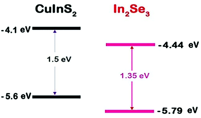
Engineering the physical and chemical properties of semiconductor nanostructures or quantum dots (QDs) has been a frontier research area for the past three decades.1–5 The efficaciousness of QDs lies in controlling their properties by tuning the size, shape and composition.6–9 In addition, the choice of an organic surfactant layer protecting the nanostructure expands the possibility of surface engineering.10,11 Though cadmium and lead based nanoparticles are verified with high applicability,12,13 their inherent toxicity calls forth environment friendly and commercially viable ‘green’ nanostructures,13–15 particularly when biomedical applications are concerned.16,17 Green QDs include I–III–VI2 compounds such as CuInS2 (CIS), CuInSe2 (CISe), and CuInSeS (CISeS) along with many other binary quantum dots which are free from heavy metals.18,19 Among these, CIS and CISe are direct band gap semiconductors with band gap onset in the NIR region.20,21 Besides, the high absorption coefficient makes them efficient in light harvesting applications.22 But, compared to the binary II–VI QDs, the slow hole scavenging and the presence of surface trap states limits the use of these I–III–VI2 nanostructures in different applications. This is due to the non-stoichiometric compositions and complex crystal structures of these nanostructures.23,24 A possible solution to overcome these issues is to passivate the surface states by an epitaxial growth of a semiconductor layer which further modifies the electronic properties of the nanostructures synthesized.24–27 Recently, Kim et al. observed that a ZnS shell over CISe core reduced non-radiative recombination and interfacial electron recombination in them.15 Similarly, Donega and coworkers reported an appreciable improvement in photoluminescence quantum yield of CIS QDs by over coating with ZnS or CdS.28,29 The same observation was also reported by Klimov and coworkers while evaluating light emission mechanisms in a CIS/ZnS core–shell system.30 Most of the reported works on CIS and CISe QDs are based on growing a ZnS passivating layer over the core to form a core/shell type-I structure.17,31–33 In some earlier attempts, In2S3 was used in conjunction with CIS thin films for improving the performance of thin film based photovoltaic systems.34,35 Also, In2Se3 has been employed as a buffer layer in devising CIS QD sensitized solar cells.36 In the present study, the effort is to grow an indium selenide (In2Se3) passivating layer over the CIS core, which not only acts as a surface passivating layer, but also results in a type-II band offset, which can confine the holes in the core and the electrons in the outer layer37 (Scheme 1). The resulting charge separation makes the material ideal for photovoltaic applications. Besides, since the lattice mismatch is less, In2Se3 is a suitable choice as a passivating layer for CIS.38 To the best of our knowledge, CIS QDs with In2Se3 as a passivating layer is not yet reported. Also, in the present study, we are adopting a phosphine free, ‘green route’ for the synthesis.18,39,40 The advantage of the colloidal method lies in its control of particle size and shape distribution with less number of defect states.33,37,41,42 Developing green chemistry alternatives in nanomaterials synthesis is a major concern of the research community.43 In our synthesis, to avoid the toxicity caused by the organophosphines, we dissolved the elemental selenium in the capping agent-coordinating solvent (oleylamine–octadecene) mixture. To grow a layer of In2Se3, the selenium coordinated to oleylamine was injected to the CIS QD dispersion. A similar type of shell growth strategy was reported from Zhong group, except that the exchange was of cations.22
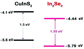 |
| | Scheme 1 Schematic representation of the energy level diagrams of CIS and In2Se3. | |
Experimental section
Materials
Copper(I) iodide (CuI, Puratronic, 99.998%), indium(III) acetate (In(OAc)3, 99.99%) were purchased from Alfa Aesar. Sulfur powder (S, 99.99%), selenium powder (Se, 200 mesh, 99.99%), oleylamine (OAm, 97%) and 1-octadecene (ODE, 90%) were purchased from Sigma-Aldrich. The chemicals were used as procured without further purification.
Characterisation
The FTIR spectrum was recorded using Perkin Elmer spectrum 400 spectrometer. The absorption spectra were recorded using a Shimadzu-3600 UV-VIS-NIR spectrophotometer. The high resolution transmission electron microscopic images of the QDs were recorded using JEOL 200 kV JEM-2100 microscope, after depositing them on carbon coated copper grids. The elemental composition was analysed with X-ray photoelectron spectroscopy (PHI 5000 Versa Probe II X-ray photoelectron spectrometer using Mg Kα radiation), inductive coupled plasma-atomic emission spectroscopy (Perkin Elmer Optima 5300 DV) and energy dispersive X-ray spectroscopy (JED-2300 analysis station). The crystal structure was studied using selected area electron diffraction pattern and X-ray diffraction analysis (Rigaku miniplex X-ray diffractometer using Cu Kα radiation). The electrochemical bandgap of the material was determined from cyclic voltammograms recorded using an Autolab 204N electrochemical workstation (Metrohm Autolab) employing a three electrode configuration with a scan rate of 50 mV s−1. In the instrument, glassy carbon was used as the working electrode, platinum wire as the auxiliary electrode and silver/silver chloride electrode as the reference electrode. Also, tetrabutyl ammonium hexafluorophosphate (0.1 M) was used as the supporting electrolyte.
Synthesis of CuInS2 QDs
Oleylamine capped CIS QDs were prepared by following a reported procedure.22 In brief, a mixture of CuI (0.038 g, 0.2 mmol), In(OAc)3 (0.058 g, 0.2 mmol), OAm (6 ml, 0.018 mmol) and 1-ODE (12 ml) were heated to 180 °C, in a three necked round bottom flask under argon atmosphere with continuous stirring until a clear pale yellow solution was obtained. At this temperature, an injection mixture containing sulphur (0.0192 g, 0.6 mmol) in OAm (0.6 ml, 0.0018 mmol) was injected into the reaction mixture and kept for 20 minutes. The OAm capped CIS QDs obtained were purified by precipitation with acetone and dispersed in chloroform.
Synthesis of CuInS2–In2Se3 QDs
To grow a thin layer of In2Se3 over the CIS QDs prepared, the dots were loaded in a round bottom flask along with 6 ml OAm and 12 ml ODE and heated to 40 °C under vacuum for 20 minutes. The vacuum was then replaced with argon and the reaction mixture was further heated to 170 °C, under constant stirring. At this temperature, 0.3 ml Se solution (0.078 g Se powder dissolved in a mixture of 1 ml OAm and 2 ml ODE) was injected into it and kept for 30 min for the growth of the In2Se3 layer over the CIS QDs. The CIS–In2Se3 QDs obtained were purified by precipitation with methanol twice and then with acetone. The nanostructures obtained were dispersed in chloroform for further studies.
Results and discussion
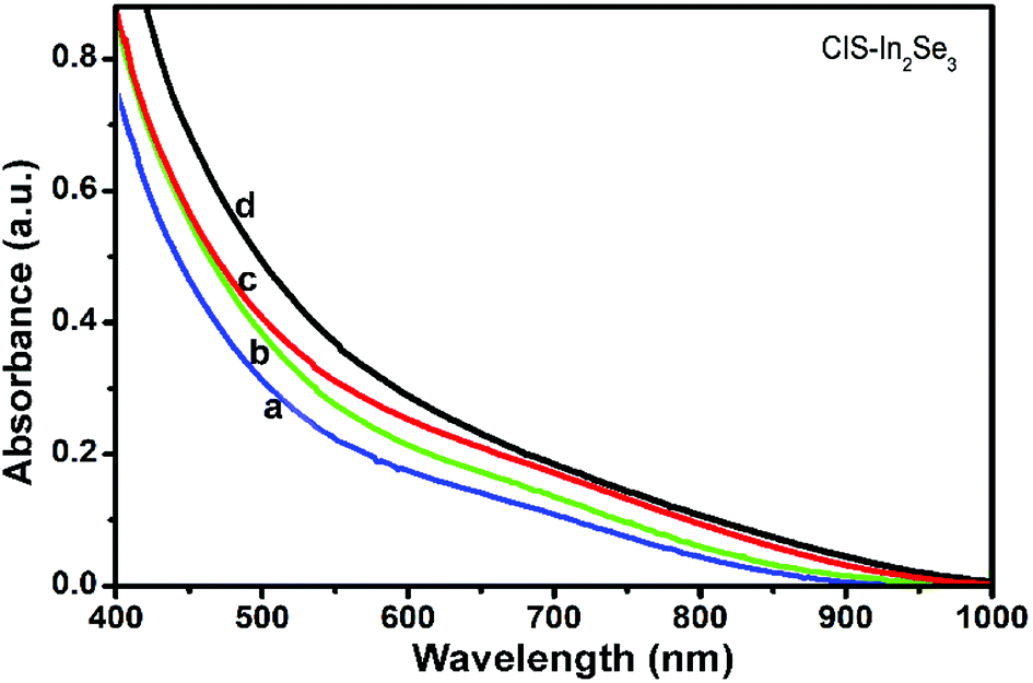
CIS–In2Se3 QDs obtained were stable and the OAm capping agent rendered them were easily dispersible is non polar organic solvents. The presence of OAm attached to the QD surface was evaluated by FTIR studies (Fig. S1†). The absorption spectra obtained for CIS–In2Se3 of different CIS QD core sizes is shown in Fig. 1. The figure shows that the over coating of CIS with In2Se3 results in a red shift in the absorption spectra, compared to that of the CIS core (Fig. S2†). The further extension of the absorption onset to the NIR region makes the material more suitable as a light harvester in photovoltaic applications. The band gap energy (Eg) of CIS and CIS–In2Se3 QDs were determined as 1.91 and 1.81 eV respectively, by Tauc plot (Fig. S3†), using the relation α = β/(hν)(hν − Eg)n, where α is the linear absorption coefficient and β is the band gap tailoring parameter constant.44–46
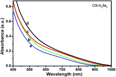 |
| | Fig. 1 Absorption spectra of CIS–In2Se3 QDs in chloroform (a → d), with increasing CIS core sizes. | |
The luminescence observed in CIS (Fig. S4†) has disappeared in CIS–In2Se3 due to the charge separation, a characteristic of a type-II system.47
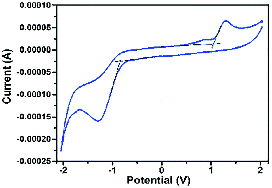
The HOMO and LUMO levels and the bandgap energy of the materials synthesized were estimated using cyclic voltammetry measurements. The HOMO and LUMO levels were calculated from the onset of oxidation peak (EOx) and reduction peak (ERed) using the following equations.39
From Fig. 2, using the oxidation and reduction peak onsets (1.05 and −0.82 eV), the HOMO and LUMO levels of the CIS–In2Se3 QDs were estimated as −5.75 and −3.88 eV respectively. This gives the band gap as 1.87 eV, which is in close agreement with the value obtained from the absorption data. Also, the band gap for CIS was estimated as 1.95 eV (Fig. S5†), which is also in agreement with optical spectral data.
 |
| | Fig. 2 Cyclic voltammograms of CIS–In2Se3 QDs. | |
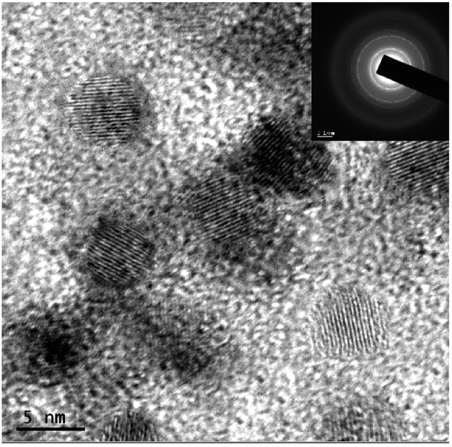
The high resolution transmission electron microscopic (HRTEM) images (Fig. 3) indicated a spherical geometry and a uniform size distribution for the CIS–In2Se3 QDs. The average grain size was estimated to be around 4.8 nm with lattice spacing (d value) 0.33 nm. The d spacing obtained corresponds to the spacing of (112) lattice planes of the tetragonal chalcopyrite structure (ICDD 36-1311). The d value was also measured from the SAED pattern (inset of Fig. 3), which also confirmed the good crystallinity of the QDs.
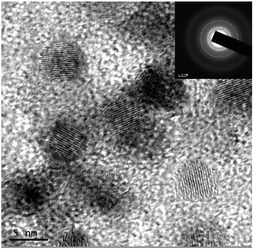 |
| | Fig. 3 High resolution TEM image of CIS–In2Se3 QDs. | |
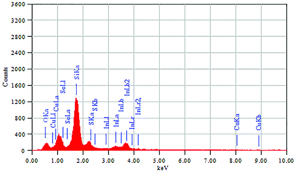
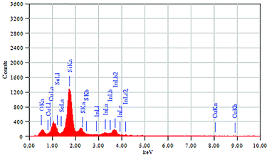
The elemental composition of the CIS–In2Se3 QDs was analysed using energy dispersive X-ray analysis (Fig. 4), with the composition ratio Cu![[thin space (1/6-em)]](https://www.rsc.org/images/entities/char_2009.gif) :In:S:Se as 1:1.1:0.7:0.34. The spectrum confirmed the presence of selenium, in addition to copper, indium and sulphur seen for the CIS QDs (Fig. S6†). Presence of selenium in the CIS–In2Se3 nanostructure was also confirmed by ICP-AES studies (data not shown).
:In:S:Se as 1:1.1:0.7:0.34. The spectrum confirmed the presence of selenium, in addition to copper, indium and sulphur seen for the CIS QDs (Fig. S6†). Presence of selenium in the CIS–In2Se3 nanostructure was also confirmed by ICP-AES studies (data not shown).
 |
| | Fig. 4 EDAX spectrum of CIS–In2Se3 QDs. | |
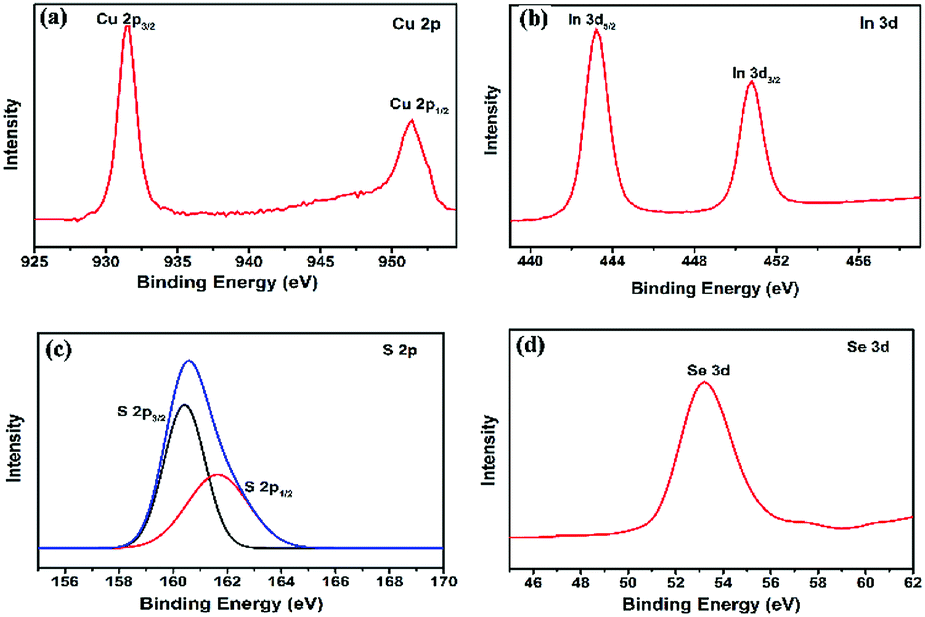
The elemental composition as well as the valence states of CIS–In2Se3 QDs were analysed by XPS. The resolved spectra, calibrated with C1s as the reference (284.60 eV) is shown in Fig. 5 (combined spectrum is shown in ESI Fig. S7†). The Cu 2p core splits into Cu 2p3/2 (931.46 eV) and Cu 2p1/2 (951.38 eV) with a peak separation 19.92 eV which is in close agreement with the standard data.48 Also, the absence of peak at 942 eV corresponding to the cuprous state, confirms the +2 oxidation state of copper.49 Peaks at 443.26 eV and 450.81 eV, separated by 7.55 eV in Fig. 5(b) is ascribed to binding energies of In 3d5/2 and In 3d3/2 which assigns a +3 oxidation state to indium.36,50 Peaks at 160.4 and 161.6 eV, separated by 1.2 eV (Fig. 5(c)), corresponds to sulphur 2p3/2 and 2p1/2, arising by spin–orbit coupling. This is an also an indication of sulphur bonded with both indium and copper.51 The peak at 53.4 eV in Fig. 5(d) is attributed to the binding energy of selenium 3d. Indium and selenium 3d spectral features are in consistence with γ-In2Se3 structural characteristics.36,50,52
 |
| | Fig. 5 High resolution XPS spectra of (a) Cu 2p (b) In 3d (c) S 2p and (d) Se 3d. | |
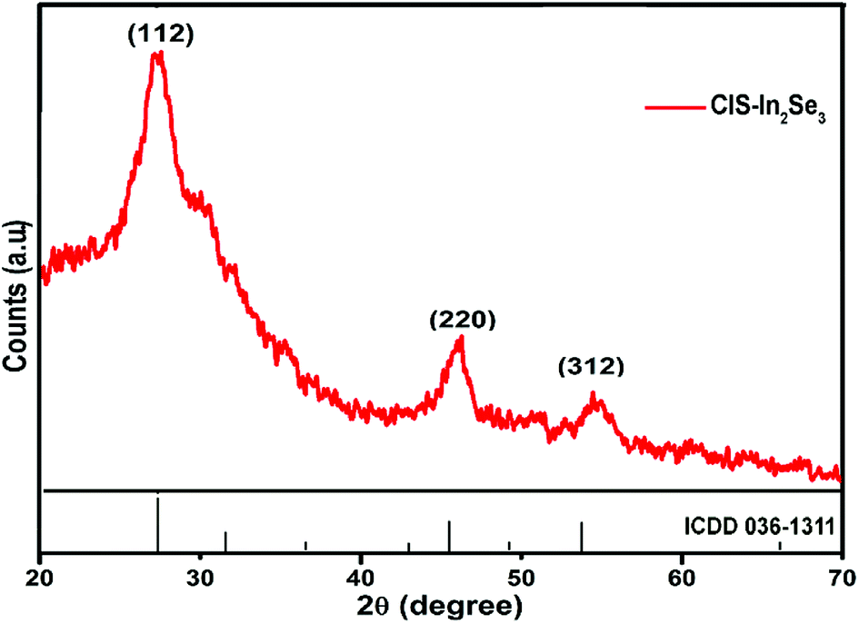
Crystalline nature of CIS–In2Se3 QDs was analysed using the X-ray diffraction pattern shown in Fig. 6 (XRD data of CIS QDs are provided in Fig. S8†). Three major broad peaks at 26.94°, 46.20° and 54.93° correspond to the (112), (220) and (312) planes with lattice constants a = b = 5.552 Å and c = 12.273 Å. The data matches well with a tetragonal chalcopyrite crystal structure (ICDD 36-1311). The size of the QDs were estimated as 4.78 nm from the XRD peaks based Debye's Scherrer formula and was found to be in good agreement with the value obtained from the TEM images.
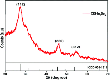 |
| | Fig. 6 X-ray diffraction (XRD) pattern of CIS–In2Se3 QDs along with standard ICDD reference. | |
Conclusions
In summary, a novel material, CuInS2–In2Se3 QDs was prepared following a two stage organometallic synthesis route. Low toxic and less expensive oleylamine was used as the ligand to make the synthesis procedure a phosphine free ‘green method’. The CIS QD core was prepared first and selenium was then introduced to grow a thin layer of indium selenide over it. The optical absorption properties were found to be superior, covering the entire visible region, extending to the NIR region, making them suitable for photovoltaic applications. The band gap values obtained from absorption data was further confirmed by CV measurements. The nanostructures were found to be spherical with well-defined lattice planes as evident from the TEM images. The chemical composition was analysed using EDAX, ICP-AES and XPS studies. XRD analysis indicated a tetragonal chalcopyrite structure for the CIS–In2Se3 QDs. The potential of this material as a light harvester is under further investigations.
Conflicts of interest
There are no conflicts to declare.
Acknowledgements
The corresponding author V. V. Ison thank SERB, DST, Govt. of India, for a fast track project (Order No. SR/FTP/PS-108/2010).
References
- M. Ye, X. Gao, X. Hong, Q. Liu, C. He, X. Liu and C. Lin, Sustainable Energy Fuels, 2017, 6, 1217–1231 RSC.
- J. Duan, H. Zhang, Q. Tang, B. He and L. Yu, J. Mater. Chem. A, 2015, 17497–17510 RSC.
- A. M. Smith and S. Nie, Acc. Chem. Res., 2010, 43, 190–200 CrossRef CAS PubMed.
- G. I. Maikov, R. Vaxenburg, A. Sashchiuk and E. Lifshitz, ACS Nano, 2010, 4, 6547–6556 CrossRef CAS PubMed.
- S. Mourdikoudis and L. M. Liz-Marzán, Chem. Mater., 2013, 25, 1465–1476 CrossRef CAS.
- J. Wang, Y. Wang, F. Cao, Y. Guo and L. Wan, J. Am. Chem. Soc., 2010, 132, 12218–12221 CrossRef CAS PubMed.
- P. M. Allen and M. G. Bawendi, J. Am. Chem. Soc., 2008, 130, 9240–9241 CrossRef CAS PubMed.
- S. Rawalekar, S. Kaniyankandy, S. Verma and H. N. Ghosh, J. Phys. Chem. C, 2011, 115, 12335–12342 CrossRef CAS.
- C. M. Donega, Chem. Soc. Rev., 2011, 40, 1512–1546 RSC.
- L. Liu, X. Guo, Y. Li and X. Zhong, Inorg. Chem., 2010, 49, 3768–3775 CrossRef CAS PubMed.
- B. Bai, D. Kou, W. Zhou, Z. Zhou, Q. Tian, Y. Meng and S. Wu, J. Power Sources, 2016, 318, 35–40 CrossRef CAS.
- H. Khattak, Journal of Undergraduate Studies at Trent (JUST), 2016, IV, 34–42 Search PubMed.
- H. K. Jun, M. A. Careem and A. K. Arof, Renewable Sustainable Energy Rev., 2013, 22, 148–167 CrossRef CAS.
- J. Du, Z. Du, J. S. Hu, Z. Pan, Q. Shen, J. Sun, D. Long, H. Dong, L. Sun, X. Zhong and L. J. Wan, J. Am. Chem. Soc., 2016, 138, 4201–4209 CrossRef CAS PubMed.
- J. Kim, J. Yang, J. H. Yu, W. Baek, C. Lee, H. J. Son and K. I. M. E. T. Al, ACS Nano, 2015, 11286–11295 CrossRef CAS PubMed.
- S. Nishimura, A. T. N. Dao, D. Mott, K. Ebitani and S. Maenosono, J. Phys. Chem. C, 2012, 116, 4511–4516 CrossRef CAS.
- L. Li, T. J. Daou, I. Texier, T. Thi, K. Chi, N. Q. Liem and P. Reiss, Chem. Mater., 2009, 21, 2422–2429 CrossRef CAS.
- C. A. M. Bonilla and V. V. Kouznetsov, ed. M. L. Larramendy and S. Soloneski, Green Nanotechnology, Overview and Further Prospects, InTech Open limited, London, 2016, pp. 182–201 Search PubMed.
- D. Sharma, R. Jha and S. Kumar, Sol. Energy Mater. Sol. Cells, 2016, 155, 294–322 CrossRef CAS.
- S. Kim, M. Kang, S. Kim, J. H. Heo, J. H. Noh, S. H. Im, S. II Seok and S. W. Kim, ACS Nano, 2013, 7, 4756–4763 CrossRef CAS PubMed.
- L. Li, A. Pandey, D. J. Werder, B. P. Khanal, J. M. Pietryga and V. I. Klimov, J. Am. Chem. Soc., 2011, 133, 1176–1179 CrossRef CAS PubMed.
- Z. Pan, I. Mora-sero, Q. Shen, H. Zhang, K. Zhao, J. Wang, X. Zhong and J. Bisquert, J. Am. Chem. Soc., 2014, 136, 9203–9210 CrossRef CAS PubMed.
- D. Aldakov, A. Lefrançois and P. Reiss, J. Mater. Chem. C, 2013, 24, 3756–3776 RSC.
- K. Zhao, Z. Pan and X. Zhong, J. Phys. Chem. Lett., 2016, 7, 406–417 CrossRef CAS PubMed.
- D. Vasudevan, R. R. Gaddam, A. Trinchi and I. Cole, J. Alloys Compd., 2015, 636, 395–404 CrossRef CAS.
- L. Li, P. Reiss and M. Protie, Small, 2009, 5, 154–168 CrossRef PubMed.
- E. A. Dias, S. L. Sewall and P. Kambhampati, J. Phys. Chem. C, 2007, 111, 708–713 CrossRef CAS.
- A. C. Berends, F. T. Rabouw, F. C. Spoor, E. Bladt, F. C. Grozema, A. J. Houtepen and C. M. Donega, J. Phys. Chem. Lett., 2016, 7, 3503–3509 CrossRef CAS PubMed.
- C. Xia, D. M. Johannes, C. G. Hans and C. M. Donega, Chem. Mater., 2017, 29, 4940–4951 CrossRef CAS PubMed.
- A. S. Fuhr, H. J. Yun, N. S. Makarov, H. Li, H. McDaniel and V. I. Klimov, ACS Photonics, 2017, 4, 2425–2435 CrossRef CAS.
- W. Li, Z. Pan and X. Zhong, J. Mater. Chem. A, 2015, 3, 1649–1655 RSC.
- J. Ma, M. Liu, Z. Li and L. Li, Opt. Mater., 2015, 47, 56–61 CrossRef CAS.
- C. Xia, J. D. Meeldijk, H. C. Gerritsen and C. M. Donega, Chem. Mater., 2017, 29, 4940–4951 CrossRef CAS PubMed.
- A. S. Cherian, T. Abe, Y. Kashiwaba, C. S. Kartha and K. P. Vijayakumar, Energy Procedia, 2012, 15, 283–290 CrossRef CAS.
- B. Asenjo, A. M. Chaparro, M. T. Gutierrez, J. Herrero and J. Klaer, Sol. Energy Mater. Sol. Cells, 2005, 87, 647–656 CrossRef CAS.
- J. Y. Chang, J. M. Lin, L. F. Su and C. F. Chang, ACS Appl. Mater. Interfaces, 2013, 5, 8740–8752 CrossRef CAS PubMed.
- S. Kim, B. Fisher, H. J. Eisler and M. Bawendi, J. Am. Chem. Soc., 2003, 125, 11466–11467 CrossRef CAS PubMed.
- Y. Q. Wang, Y. C. Rui, Q. H. Zhang, Y. G. Li and H. Z. Wang, ACS Appl. Mater. Interfaces, 2013, 5, 11858–11864 CrossRef CAS PubMed.
- S. Cao, W. Ji, J. Zhao, W. Yang, C. Li and J. Zheng, J. Mater. Chem. C, 2016, 4, 581–588 RSC.
- C. Pu, J. Zhou, R. Lai, Y. Niu, W. Nan and X. Peng, Nano Res., 2013, 6, 652–653 CrossRef CAS.
- E. H. Sargent, Adv. Mater., 2005, 17, 515–522 CrossRef CAS.
- S. B. Brichkin and V. F. Razumov, Russ. Chem. Rev., 2016, 85, 1297 CrossRef CAS.
- Y. Pu, F. Cai, D. Wang, J. X. Wang and J. F. Chen, Ind. Eng. Chem. Res., 2018, 57, 1790–1802 CrossRef CAS.
- P. Taylor, E. A. Davis and N. F. Mott, Philos. Mag., 2006, 22(179), 0903–0922 Search PubMed.
- J. Tauc, Amorphous and Liquid Semiconductor, Plenum Press, New York, 1974 Search PubMed.
- J. Tauc, Mater. Res. Bull., 1968, 3, 37–46 CrossRef CAS.
- J. E. Halpert, V. J. Porter, J. P. Zimmer and M. G. Bawendi, J. Am. Chem. Soc., 2006, 128, 12590–12591 CrossRef CAS PubMed.
- F. Yuan, B. Chiu, T. Kao, C. Lai and H. Tuan, Energy Environ. Sci., 2011, 4, 4929–4932 RSC.
- H. Zhong, Y. Li, M. Ye, Z. Zhu, Y. Zhou, C. Yang and Y. Li, Nanotechnology, 2007, 18, 2–8 Search PubMed.
- S. Rengaraj, S. Venkataraj, C. W. Tai, Y. Kim, E. Repo and M. Sillanpää, Langmuir, 2011, 27, 5534–5541 CrossRef CAS PubMed.
- M. Chiang, S. Chang, C. Chen, F. Yuan and H. Tuan, J. Phys. Chem. C, 2011, 5, 1592–1599 CrossRef.
- S. Yang, C. Y. Xu, L. Yang, S. P. Hu and L. Zhen, RSC Adv., 2016, 6, 106671–106675 RSC.
Footnote |
| † Electronic supplementary information (ESI) available. See DOI: 10.1039/c8ra07389a |
|
| This journal is © The Royal Society of Chemistry 2018 |
Click here to see how this site uses Cookies. View our privacy policy here. 
 Open Access Article
 This Open Access Article is licensed under a Creative Commons Attribution-Non Commercial 3.0 Unported Licence
 a,
Libin Kuriakose
a,
Libin Kuriakose