
Linking structural properties with functionality in solar cell materials – the effective mass and effective density of states†
Thomas
Kirchartz
 *ab and
Uwe
Rau
a
*ab and
Uwe
Rau
a
aIEK5-Photovoltaics, Forschungszentrum Jülich, 52425 Jülich, Germany. E-mail: t.kirchartz@fz-juelich.de
bFaculty of Engineering and CENIDE, University of Duisburg-Essen, Carl-Benz-Str. 199, 47057 Duisburg, Germany
First published on 8th May 2018
Abstract
Understanding crucial material properties making a certain material suitable for a specific application requires a clear methodology linking microscopic parameters with macroscopic functionality. This paper provides such a methodology for the relevant example of the effective mass or effective density of states in semiconductors used as photovoltaic absorber materials. This example is inspired by the recent suggestion that low effective masses are a crucial ingredient explaining the high efficiency and in particular the high open-circuit voltages in metal-halide perovskite solar cells. We critically examine this claim and discuss the conditions that affect the relation between basic properties of a band structure with photovoltaic or more generally optoelectronic functionality. While low effective masses may indeed have a beneficial effect on the open-circuit voltage in the non-radiative limit, using low effective masses as a generic criterion for high optoelectronic functionality would be an oversimplification. Instead the effective mass should always be considered in combination with other material or device specific properties such as the type of band gap (direct or indirect), the doping level and the dominant carrier scattering mechanism.
1. Introduction
During recent years, metal-halide perovskites have written an unprecedented success story as materials for solar cells1–6 and light-emitting diodes.2,7–12 Achieving solar cell efficiencies above 20% (ref. 13–16) within less than 5 years of development naturally puts the question on the agenda whether very specific properties17,18 give metal-halide perovskites an advantage over other materials that have been studied for decades with only a few material technologies achieving the same efficiency level as the perovskites.19Furthermore, important lessons learned from the metal-halide perovskites may help to develop general design principles for a successful systematic search for new photovoltaic absorber materials. Nowadays, computational materials research enables us to systematically scan entire material classes by first principle calculations for promising candidates optimally suited for various applications, e.g. as photovoltaic absorber materials.20–22 However, the success of such a computational approach critically relies on the correct definition23 of target properties allowing distinction of hopeful candidates from the hopeless ones.24,25
Recently, the low effective mass26 and consequently the low density of electronic states in the valence band and conduction band found experimentally27,28 and theoretically29–31 for lead halide perovskites has been named as a possible ingredient to the success of metal-halide perovskites.32 In addition, the band structure may involve direct and indirect transitions in a very close energy range which has also been claimed to be beneficial for photovoltaic efficiency.33–36 Given that the effective mass or effective density of states are features of the band structure that are always calculated in the context of computational material screening efforts, it is of huge relevance for the community investigating novel materials for photovoltaics, whether these basic features of semiconductor band structures would be beneficial for photovoltaics at least on the level of theory where parabolic approximations to the energy vs. momentum relations of the bands are sensible. A detailed look at the key properties of solar cell absorber material, i.e. absorption, charge transport and recombination reveals that the effective mass or effective density of states enters a large number of equations that potentially affect device performance. Thus, the purpose of this manuscript is to start a systematic discussion of the effect of the key features of simple parabolic bands on photovoltaic materials. A closer look at the influence of band structure on absorption and non-radiative recombination quickly reveals that performance depends on whether the semiconductor is direct or indirect as well as whether the material is doped or intrinsic. Thus, in order to achieve a systematic discussion of the effects, we distinguish between these four combinations of a direct/indirect and doped/intrinsic semiconductor for all our simulations. The key results of our study are that in three out of four cases, low effective masses would indeed lead to slightly higher efficiencies at infinite mobilities. However, these higher efficiencies would be reached at substantially higher optimum thicknesses and depending on the exact scattering mechanism dominating mobility, higher effective masses might be often be more beneficial in realistic situations of finite mobilities and ideally low absorber thicknesses.
2. Definitions of effective mass and effective DOS
The purpose of this paper is to study the relation between structural properties and device functionality on a level of abstraction that allows us to draw conclusions as a function of a limited number of parameters. The methodology that we establish will then also be transferrable to situations with a reduced level of abstraction. Thus, we will assume that we can treat our semiconducting photovoltaic absorber material of interest by approximating the energy vs. momentum relation of its conduction and valence band with a parabola. In the following, we will briefly repeat the relevant equations that can also be found in various textbooks (see e.g.ref. 37). Near the conduction band edge the relationship between the energy E and momentum k of an electron in the conduction band can be approximated by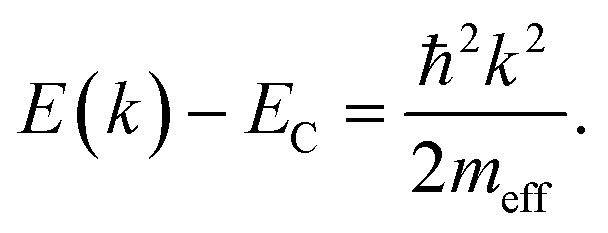 | (1) |
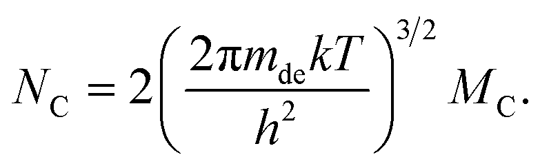 | (2) |
Analogous equations can of course be written down for the valence band effective hole mass and effective density of states. For the purpose of this paper, we will restrict ourselves to the simplest case, where the effective mass is the same in all directions of k-space and the same for the conduction and valence band. In this simplified situation, we can just talk of effective mass and effective density of states without distinguishing the direction of k-space or the band. We also note that while many semiconductors have dispersion relations that become non-parabolic away from the conduction band minimum or valence band maximum, most of the parameters we discuss here are most strongly related to the region of the band very close to the band edges. For instance, the effective density of states is related to the energy dependent density of states close (within a few kT) to the band edges. The absorption coefficient for a material suitable for high efficiency photovoltaics should increase within a few kT above the band gap to values that lead to complete absorption. Thus, even if the parabolic approximation is unsuitable over a range of hundreds of meV, it would not or not strongly affect the discussion using parabolic bands. Anisotropy in effective masses would affect the results but it would still be relatively straightforward to adapt the methodology to more complicated dispersion relations, while it would be outside the scope of the present work to discuss all possible variations of effective mass anisotropy or variations between conduction and valence band effective masses.
3. Classical arguments in favor of low effective masses
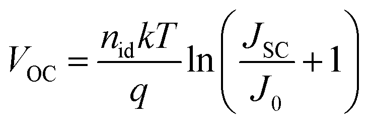
There are two classical arguments in favour of low effective masses and densities of states. The first argument is based on the relation between the effective density of states and the open-circuit voltage VOC. For the case of a position independent splitting between the quasi-Fermi energies EFn and EFp for electrons and holes it is fair to write32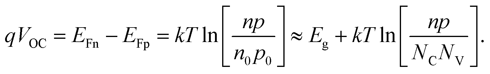 | (3) |
In eqn (3), q is the elementary charge, n, p are the concentrations and n0, p0 the equilibrium concentrations of electrons and holes. The product n0p0 is connected to the intrinsic carrier concentration ni and to the effective densities NC and NV of states in the conduction and valence band via
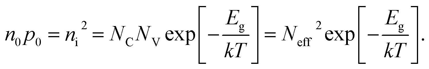 | (4) |
A cursory look at eqn (3) and (4) might suggest that a lower effective density of states implies a higher VOC by tacitly assuming a constant np product for the comparison.32
This is fair if everything else was kept constant including in particular the absorption coefficient. However, also the absorption coefficient is a function of the available density of states for the optical transitions. Because the product np is a result of the photogeneration and recombination of free charge carriers this will affect VOC and also other photovoltaic properties (like the short-circuit current).
The second frequently made comment about the beneficial influence of the effective mass is based on the idea that larger effective masses reduce the mobility. This is indeed typically the case but depends on the scattering mechanism dominating the mobility in a particular material in the temperature range of interest. However, higher absorption coefficients for higher effective masses would require lower thicknesses for complete absorption and lower thicknesses in turn would require lower mobilities for complete charge carrier collection. Thus, it is not a priori clear whether low effective mass materials are generally better than high effective mass materials but instead a more detailed and quantitative analysis is required.
4. Parameters affected by the effective mass or density of states
In the following, we will briefly discuss how the effective mass affects the key properties of any photovoltaic absorber material, namely the absorption coefficient α, the lifetime τ or recombination rate R and the mobility μ. Table 1 provides the key relationships that hold on the level of theory, discussed here, where parabolic bands are still appropriate. Table 1 uses proportionality signs to highlight the effect of effective mass or density of states and to reduce the level of complexity. Table S1 in the ESI† provides the same information but now without proportionality signs, also discussing the prefactors as far as this is possible.| Quantity | Dependence on effective mass meff or effective DOS Neff (m denotes the free electron mass) |
|---|---|
| Absorption coefficient αdir (direct semiconductor) |
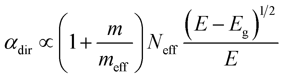 (ref. 38 and 73) (ref. 38 and 73) |
| Absorption coefficient αind (indirect semiconductor) |
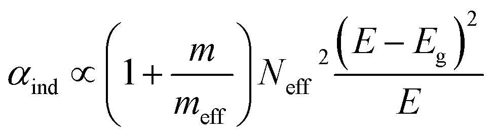 (ref. 38 and 74) (ref. 38 and 74) |
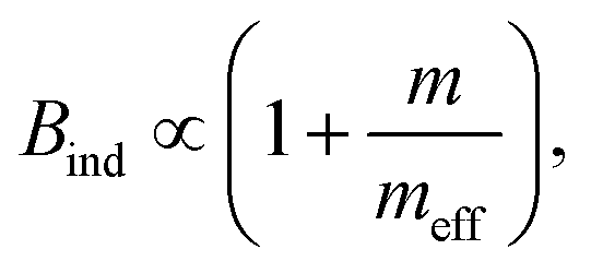
| Radiative recombination coefficient Bdir (direct semiconductor) |

|
| Radiative recombination coefficient Bind (indirect semiconductor) |
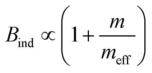
|
| SRH recombination rate RSRH (low level injection) |
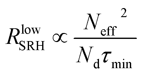
|
| SRH recombination rate RSRH (high level injection) |
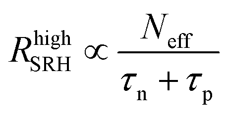
|
| Capture cross section (for multiphonon transitions) |
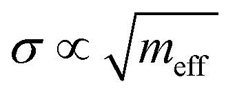 (ref. 43,75 and 76) (ref. 43,75 and 76) |
| Thermal velocity |
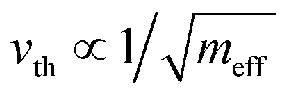
|
| SRH lifetime (for multiphonon transitions) | τ = (σvthNt)−1 = const. |
| Mobility μ |
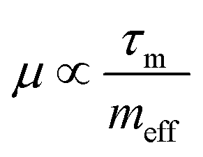 (ref. 57) (ref. 57) |
| Momentum relaxation time for lattice scattering |
 (ref. 57) (ref. 57) |
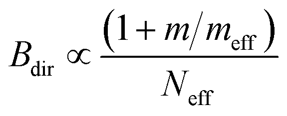
The absorption coefficient α depends on the density of available states – linearly for a direct semiconductor (αdir ∝ Neff) and on the product of the densities of states of valence and conduction band for an indirect semiconductor (αind ∝ Neff2). The influence of the effective density of states is stronger for indirect than for direct semiconductors because the k-selection rule is relaxed for indirect transitions due to the influence of phonons. In addition, the absorption coefficient is proportional to the squared momentum matrix element pCV2 that is given for simple parabolic bands by pCV2 = mEg/2 × (1 + m/meff),38 where m is the free electron mass. These two effects combined yield the proportionalities given in Table 1.
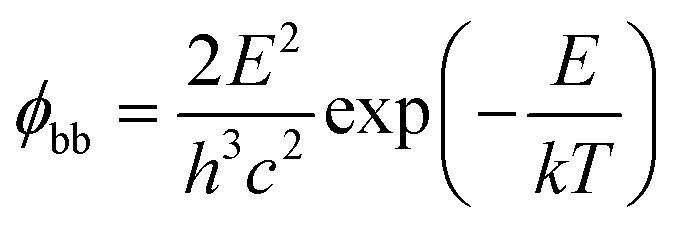
Radiative recombination is linked to absorption by the principle of detailed balance. The radiative recombination rate is typically written as Rrad = B(np − n0p0) where B denotes the radiative recombination coefficient. The thermal equilibrium value Bn0p0 of the radiative recombination rate is linked to the absorption coefficient α via the van Roosbroeck–Shockley relation39
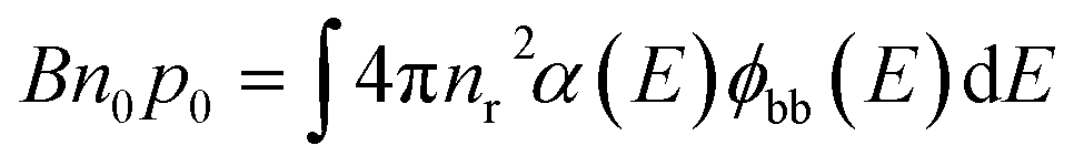 | (5) |
 | (6) |
 | (7) |
 | (8) |
In the next step, we consider non-radiative recombination via Shockley–Read–Hall (SRH) recombination40,41 with the recombination rate
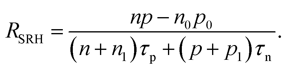 | (9) |
For recombination via deep mid-gap states the reference concentrations n1 and p1 (ref. 42) are small compared to the free carrier concentrations. For low-level injection conditions we have n ≫ n1,n0 and p = p0 = Nd ≫ p1, n, i.e., the hole concentration (assumed to be the majority carrier concentration without loss of generality) equals the doping concentration Nd. The dependence of the SRH recombination rate on the split of the quasi-Fermi levels EFn − EFp is then given by
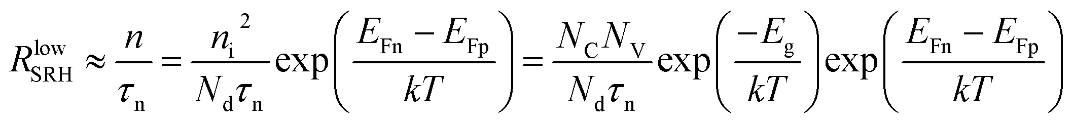 | (10) |
For high injection conditions we have n ≫ n1,n0, p ≫ p1,p0, and n ≈ p (charge neutrality). With these assumptions we get
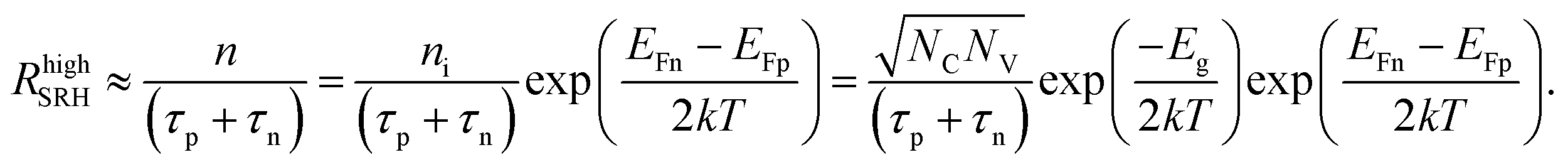 | (11) |
Having summed up the dependence of the basic photovoltaic actions, i.e. light absorption as well as radiative and non-radiative recombination, on the density of states at the edges of the conduction and valence band we are now able to calculate the influence of these densities of states on the efficiency potential of the solar cell using a basic detailed balance model.24
5. Efficiency calculations
5.1 Radiative efficiencies
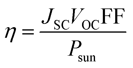
To calculate the efficiency potential from the given material parameters we follow the method outlined in ref. 24. In a first step, we will calculate the radiative efficiency for high mobilities and in section (b), we will look at the efficiency in the presence of SRH recombination but still for high mobilities. Incomplete charge collection due to low mobilities is then discussed in Section 7.The conversion efficiency η is given by44
 | (12) |
 | (13) |
 | (14) |
 | (15) |
Note that for the calculation of the absorptance spectrum A(E) from a given absorption coefficient α(E) we need to make an assumption of the specific light trapping structure.24 In the present work we refer to a Lambertian light trapping scheme for all calculations with the equations given in ref. 48 which has proven in the past to be a useful standard to compare the photovoltaic potential of different photovoltaic absorber materials.24 We assume for the moment that the carrier mobilities are high enough to warrant perfect carrier collection implying the electron and hole Fermi-levels are flat throughout the absorber for any bias condition. Furthermore, we consider the situation where the optical absorption and emission is strictly limited to energies above the band gap energy Eg.
5.2 Efficiencies in the presence of non-radiative recombination
While efficiency and JSC are calculated using the same equations as for the radiative limit, we have to use a different saturation current density. In the following, we will restrict ourselves to the simple case, where the lifetimes for electrons and holes are the same, i.e. τn = τp = τ. The recombination current in the limit of high mobilities is given by J = qRd, where the recombination rate R = n/τ in low level injection (eqn (10)) and d is the thickness. The saturation current density is given as the voltage independent prefactor and can thus be written in low level injection (doped semiconductor) as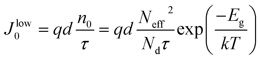 | (16) |
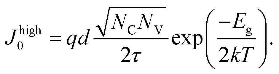 | (17) |
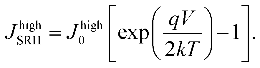 | (18) |
Note that we assume in this paper that bulk recombination is dominating the saturation current density and we neglect surface recombination for simplicity. Note, however, that surface recombination would change the way J0 depends on thickness in a rather complicated way.49,50
6. Results for infinite mobilities
In the following, we use the equations introduced in chapter 5 to calculate the efficiencies in the radiative limit and in the presence of non-radiative recombination for the four cases we distinguished above: direct and indirect band gap semiconductors both either for low or high level injection (i.e. high or low doping density). Initially, we assume the mobilities to be sufficiently high so that charge collection is always perfect. The parameter for the optical properties are given in Table S2 in the ESI† (columns generic direct and generic indirect) and the SRH lifetime is τn = τp = 1 μs. Even in this idealized high-mobility situation, efficiencies will depend on the thickness of the absorber layers. For low thicknesses, light is not efficiently absorbed and the short-circuit current is reduced. In the radiative limit, this reduction at low thicknesses is the only relevant effect and efficiency therefore just saturates if thicknesses are sufficiently high for the absorptance to resemble the ideal step-function. If non-radiative bulk recombination is dominant, the dark saturation currents increase linearly with thicknesses (cf.eqn (16) and (17)) and therefore, the efficiency will start decreasing once the short-circuit current is in saturation. Therefore, in the presence of non-radiative recombination, we expect to observe a finite optimum thickness even for infinite mobilities.Fig. 1 shows the efficiency for the four cases discussed as a function of thickness for five different values of the effective density of states (Neff = 1018, 1018.5, 1019, 1019.5, 1020 cm−3). The dashed lines always correspond to the radiative limit. Here, we observe that the saturation value η = 30.5% at high thicknesses is independent of effective DOS and identical to the Shockley–Queisser limit51 at a band gap Eg = 1.6 eV. This observation is consistent with the Shockley–Queisser limit being independent of internal properties such as effective DOS or effective mass. At lower thicknesses, however, we observe differences that are due to the different absorption coefficients. The higher the effective DOS, the higher the absorption coefficient will be. Therefore lower thickness will be sufficient to absorb the same amount of light and, thus, the efficiency remains high for lower thicknesses as opposed to the cases with lower effective DOS. This is true for all four situations (a)–(d).
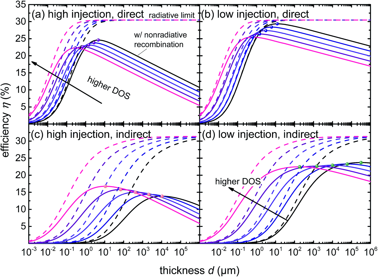 | ||
| Fig. 1 Simulated photovoltaic efficiency as a function of thickness and with the effective density of states as parameter (Neff = 1018, 1018.5, 1019, 1019.5, 1020 cm−3) for four different cases: the cases are all combinations of high and low level injection (intrinsic and doped semiconductor) and direct and indirect band gap semiconductors. The parameters for the absorption coefficient are described in Table S2† and the SRH lifetime is τn = τp = 1 μs. The dashed lines represent the radiative limit and saturates at high thicknesses towards the SQ-limit at a band gap of 1.6 eV (ηSQ = 30.5%). The solid lines also consider non-radiative recombination leading to lower VOCs at high thicknesses (cf. Fig. S2†) and therefore the efficiency reaches a maximum at a finite optimum thickness (closed symbols, also see Fig. 2). Note the corresponding range of effective masses is 0.11m up to 2.53m, where m is the free electron mass. | ||
In the presence of non-radiative recombination, we observe a decrease of the efficiency relative to the radiative limit which increases towards higher thicknesses.52 This increase does not occur in the radiative limit because the increased generation of photons in an increasing absorber volume is compensated by absorption of these photons by the absorber itself (photon recycling).53 In the radiative limit, peak efficiencies are always the same (the Shockley–Queisser limit) and efficiencies at lower thicknesses will always be highest whenever the effective DOS is highest (and therefore the absorption coefficient). In contrast, in the presence of non-radiative recombination the trend with effective DOS depends on the mode of comparison. If for instance we focus on Fig. 1a, the case of a direct semiconductor in high level injection (undoped semiconductor), we see that for low thicknesses higher DOS are beneficial. For high thicknesses, however, lower effective DOS are more beneficial because now the effect of DOS on absorption coefficient has become irrelevant while the positive effect of effective DOS on recombination is still relevant. In order to summarize the data in Fig. 1 in a way that is independent of the arbitrary choice of a constant thickness, we always determine the optimum efficiency as a function of thickness (marked with symbols in Fig. 1).
Fig. 2 presents (a) the efficiencies and (b) the optimum thicknesses calculated for a higher number of effective DOS values. From Fig. 2a we see that in three out of four cases, the lower effective DOS values indeed lead to the higher efficiencies. However, these are reached at higher optimum thicknesses as shown in Fig. 2b. If we compare the four presented cases, we observe that in case of an indirect band gap the higher effective DOS are generally favored as opposed to the direct band gap case. This is due to the stronger dependence of αind ∝ (1 + m/meff)Neff2 on Neff relative to αdir ∝ (1 + m/meff)Neff. In addition, the low injection case (doped) is in most situations (except for indirect band gaps and Neff > 1020 cm−3) better than the high injection case (intrinsic). This is due to the low injection case reaching higher fill factors and often also higher open circuit voltages by avoiding the nid = 2 recombination process, present in the high injection case.54
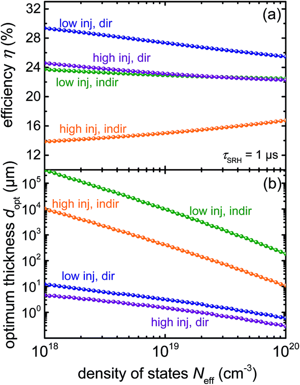 | ||
| Fig. 2 (a) Optimum efficiency and (b) the corresponding optimum thickness as a function of effective density of states for the four cases discussed in Fig. 1. The data includes non-radiative recombination and is consistent with the symbols in Fig. 1 but more data points are used for the calculation. | ||
The product αdopt of optimum thickness and absorption coefficient is approximately constant as a function of the effective density of states Neff: an increase in absorption coefficient by a factor of 10 would lead to a factor 10 lower optimum thickness. Note that αdopt is only independent of Neff but not of other parameters in the model (like direct. vs. indirect band gap). This leads to, e.g., the short-circuit current density Jsc and the light outcoupling efficiency pe being roughly constant with Neff if we always look at the optimum thickness (see Fig. S3 in the ESI†). If we are sufficiently far away from the radiative limit that we can neglect photon recycling, the external light emitting diode quantum efficiency Qlume is related to the internal quantum efficiency Qlumi, the ratio between the radiative and the total recombination rate, via53,55
 | (19) |
In addition, the open-circuit voltage VOC depends on the open-circuit voltage VradOC in the radiative limit via46,55,56
qVOC = qVradOC + kT![[thin space (1/6-em)]](https://www.rsc.org/images/entities/char_2009.gif) ln{Qlume} ≈ qVradOC + kTln{peQlumi}. ln{Qlume} ≈ qVradOC + kTln{peQlumi}. | (20) |
The outcoupling efficiency pe is a function of thickness as shown in ref. 53 and can be calculated using eqn (25) in ref. 55. Thus, we can understand the behavior of VOC(dopt) as shown in Fig. 3a by looking at the trend in Qlumi with dopt. For the case Qlumi ≪ 1 we have
 | (21) |
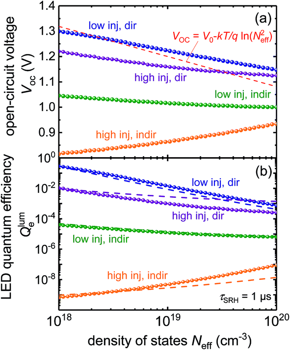 | ||
| Fig. 3 (a) Open-circuit voltage and (b) external LED quantum efficiency at the point of optimum photovoltaic efficiency as a function of effective density of states for the same four cases as discussed in Fig. 1 and 2. The symbols indicate the data from the simulations and the dashed lines in (a) represent the simplistic approximation in eqn (3) (with np = const) that does not reproduce the data while the dashed lines in panel (b) represent the analytical predictions for the internal LED quantum efficiency given in Table 2 that do reproduce the different trends rather well. By comparison between Fig. 2a and 3 it becomes clear that the trend of efficiency vs. effective DOS is mostly controlled by the trend in VOC at the optimum thickness while JSC varies from case to case but remains mostly constant with Neff within one scenario (see Fig. S3†). | ||
| High level injection | Low level injection | |
|---|---|---|
| Direct gap | Q lumi ∝ (1 + m/meff) |
|
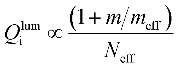
| Indirect gap | Q lumi ∝ (1 + m/meff)Neff | Q lumi ∝ (1 + m/meff) |
Fig. 3b shows the calculated Qlume (solid lines) and the analytical approximation for ∝Qlumi from Table 2 (dashed lines) for the four cases from Fig. 1 and 2. The dashed and solid lines approximately agree with each other but the agreement lacks precision in some cases because pe may change slightly with Neff as shown in Fig. S3.† This is in particular true for the high injection, indirect band gap case (orange). As expected from eqn (20), there is an obvious agreement between the trends in Qlume and Qlumi (Fig. 3b) and the trends in VOC(dopt) shown in Fig. 3a. Thus, trends in efficiencies (Fig. 2a) and open circuit voltages (Fig. 3a) are reasonably well explained by the relations presented in Table 2, rather than by the naive picture given by eqn (3).
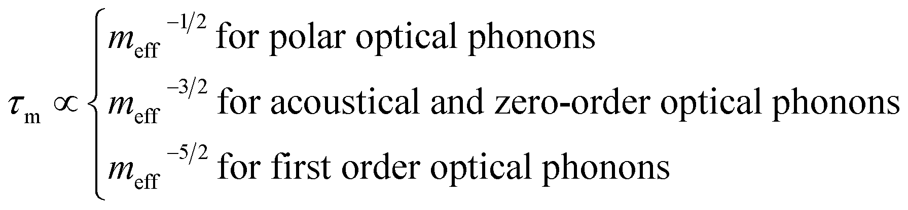
7. Effect of effective mass on charge collection
One of the key arguments in favor of low effective mass materials is based on the advantageous effect of low effective masses on charge-carrier mobilities. The mobility μ is proportional to the ratio between the momentum relaxation time τm and the effective mass (i.e. μ ∝ τm/meff).57 The momentum matrix element depends on the dominant scattering process and there are a range of different dependencies of τm on meff as shown in Table 1.57 If we focus on lattice scattering, we observe the cases τm ∝ meff−1/2 for polar optical phonons, τm ∝ meff−3/2 for acoustical phonons and zero order optical phonons and τm ∝ meff−5/2 for first order optical phonons.57 However, charge collection not only depends on mobility but also on the lifetime (which in case of non-radiative recombination via phonons is independent of effective mass) and more importantly the thickness of the absorber layer. In case of charge collection within the neutral base of a doped semiconductor, charge collection would depend mostly on the ratio between the diffusion length and the thickness d of the absorber layer.44,58,59 In contrast, if charge collection was dominated by drift rather than diffusion, it would depend on the ratio between the drift length Ldrift = μτF and the absorber thickness.60–62 Here, F is the electric field, which in the absence of strong band bending would be given by F = (Vbi − V)/d, where Vbi is the built-in voltage and V is the applied voltage. Thus, if we only consider the mobility μ and the optimum thickness dopt as the two parameters that depend on effective mass, we obtain
 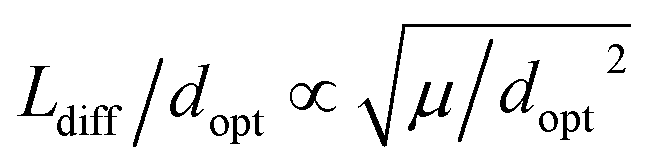 and Ldrift/dopt ∝ μ/dopt2. Collection is therefore in first approximation a non-linear function63,64 of the ratio μ/dopt2 independent of what mechanism (drift or diffusion) exactly controls recombination and transport. Thus, we compare in the following how a figure of merit (FOM) for charge collection given by this ratio (FOM = μ/dopt2) depends on effective mass or effective DOS.
Fig. 4 shows the FOM = μ/dopt2 as a function of the effective DOS for different relations between the mobility and the effective mass: (a) μ ∝ meff−3/2, (b) μ ∝ meff−5/2, and (c) μ ∝ meff−7/2. The value for the FOM = μ/dopt2 is always normalized to one for Neff = 1018 cm−3. Depending on the ratio between μ and meff, and depending on whether we are dealing with a direct or an indirect band gap, FOM = μ/dopt2 may be increasing or decreasing with Neff. The type of band gap has a strong influence on the relation between absorption coefficient and therefore optimum thickness and Neff. Thus, in case of the indirect band gap semiconductors, higher Neff are always better, because the lower optimum thickness compensates the decrease in mobility. For the direct band gap cases, the situation is less clear. Here it depends on the relation between μ and meff. For μ ∝ meff−3/2, high Neff is still more favourable, while for the two other cases (μ ∝ meff−5/2 and μ ∝ meff−7/2) high Neff leads to lower FOM = μ/dopt2.
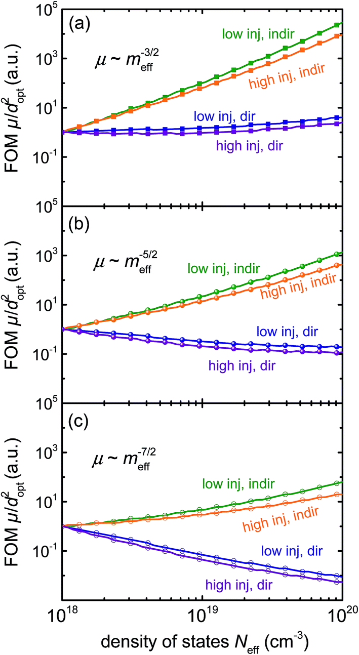 | ||
| Fig. 4 Dependence of the figure of merit μ/dopt2 for charge collection on the effective density of states for three different functional dependencies of the mobility on the effective mass: (a) μ ∝ meff−3/2, (b) μ ∝ meff−5/2, and (c) μ ∝ meff−7/2. While lower meff means higher mobility, it also means higher optimum thickness and therefore, the ratio may increase or decrease with Neff or meff depending on the dominant scattering model and the type of band gap. Low injection vs. high injection is however not a strong factor. | ||
To illustrate the meaning of the FOM = μ/dopt2 with respect to solar cell efficiencies, we used drift-diffusion simulations using the software ASA65,66 for two representative cases. Fig. 5a shows the efficiency as a function of thickness for μ ∝ meff−3/2 for two values of the effective DOS (Neff = 1018 and 1020 cm−3) and the high injection, direct band gap scenario. In addition, we varied the mobility μ0 at meff = m to show how sensitive the situations are with respect to lowering the mobility. Fig. 5b shows the equivalent simulation for the case μ ∝ meff−7/2. For both Fig. 5a and b, the high mobility cases are approximately identical to Fig. 1a (black and pink line). In case of (a) μ ∝ meff−3/2, Fig. 4 indicates that the FOM = μ/dopt2 hardly changes with Neff. Thus, the effect of lowering μ0 is comparable but the whole set of curves is shifted horizontally. In case of (b) μ ∝ meff−7/2, the FOM = μ/dopt2 decreases strongly with higher Neff (purple line in Fig. 4c). Thus, in Fig. 5b, the region of high efficiency on the thickness axis is much larger for a given μ0 if the effective DOS is low. The numerical simulations also show that the differences in absolute efficiency at the peaks of the curves are relatively small as compared to the differences in efficiency, if the device is slightly too thick or too thin, i.e. out of the optimum region that is defined by the absorption coefficient on the low thickness side and μτ/d2 on the high thickness side.
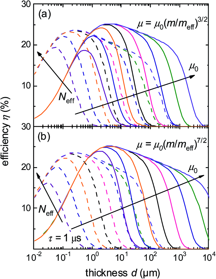 | ||
| Fig. 5 Numerical drift-diffusion simulations as a function of thickness for the case of a direct semiconductor in high level injection for two different effective densities of states (Neff = 1018 and 1020 cm−3), two different scattering models ((a) μ ∝ meff−3/2, (b) μ ∝ meff−7/2) and 5 different mobility prefactors (μ0 = 10−3, 10−2, …103, 104 cm2 V−1 s−1). The data for high mobilities corresponds approximately to Fig. 1a (black and pink line) which deals with the infinite mobility case in an analytical approximation. In the case of (a), the FOM in Fig. 4a is nearly identical for both Neff values. Thus the effect of lowering μ0 is similar but shifted in thickness. In the case of (b) the FOM in Fig. 4c is much higher (better) in case of the low Neff, thus we notice a broader shoulder for the low Neff (solid lines) and a shallower one for the high Neff (dashed lines). | ||
Fig. 6 shows the equivalent data to Fig. 5 but for the case of low level injection (Ndop = 1017 cm−3) and an indirect bandgap, i.e. a situation as encountered in crystalline Si solar cells. Now the absorption coefficient is much lower and the optimum thicknesses correspondingly higher. We chose unlike in the rest of the paper a lifetime of τ = 100 μs (1 μs everywhere else) to keep the necessary mobilities in a more realistic range. Again, we always show two values of the effective density of states (Neff = 1018 and 1020 cm−3) in each panel, while panel (a) deals with a moderate dependence of mobility on effective mass (μ ∝ meff−3/2), and panel (b) deals with a rather strong dependence of mobility on effective mass (μ ∝ meff−7/2). The mobility prefactors used are here (μ0 = 10−1, 100, 101, 102 cm2 V−1 s−1). Note that the FOMs that correspond to the situation shown in Fig. 6 are given by the green lines in Fig. 4a and c. Consistent with the trend in the FOMs in Fig. 4, in panel (a), the high effective DOS is substantially more beneficial than the lower DOS, while in panel (b) the high DOS is still better but only by a small margin.
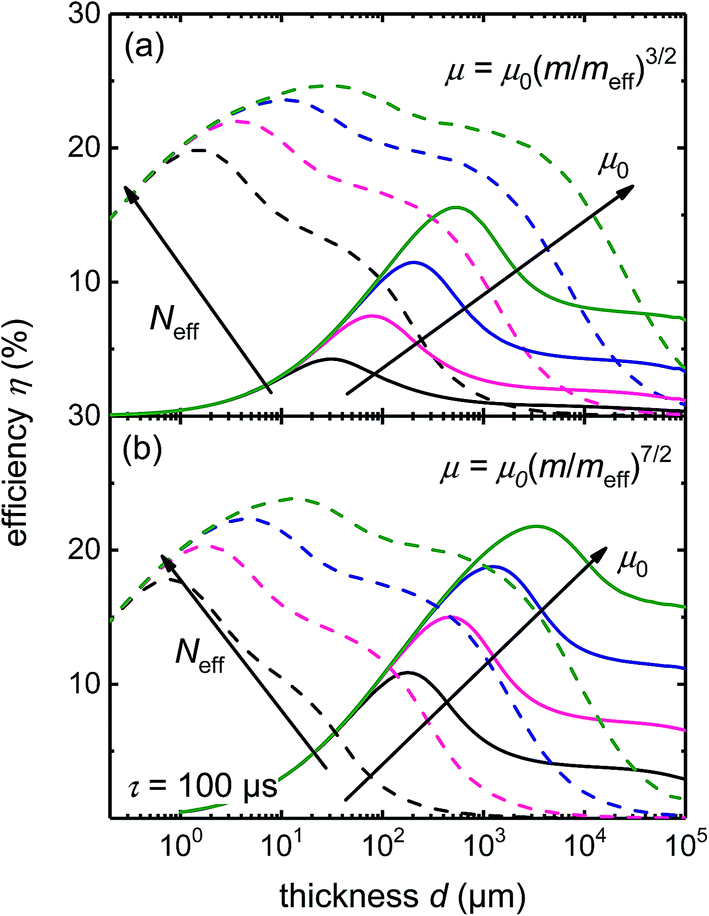 | ||
| Fig. 6 Numerical drift-diffusion simulations as a function of thickness for the case of an indirect doped semiconductor (Ndop = 1017 cm−3) for two different effective densities of states (Neff = 1018 and 1020 cm−3), two different scattering models ((a) μ ∝ meff−3/2, (b) μ ∝ meff−7/2) and 4 different mobility prefactors (μ0 = 10−1, 100, 101, 102 cm2 V−1 s−1). The lifetime was set to 100 μs to keep the mobilities necessary for efficient collection at the relatively higher thicknesses in a realistic range. The corresponding FOMs are given by the green lines in Fig. 4a and c. The FOMs explain why in the case displayed in panel (a), the high effective DOS is substantially more beneficial than the lower DOS. In panel (b) the high DOS is still better but only by a small margin. | ||
8. Summary and conclusions
The first result of the present paper is that there is no simple answer to the question whether high or low densities of states in the conduction or valence band of a photovoltaic absorber material are preferred. The primary photovoltaic interaction, light absorption by the generation of electron hole pairs, is enhanced by a high density of states. In the radiative limit, this advantage is counterbalanced by the fact that radiative recombination is strengthened by high densities of states in the same way as the light absorption.39 Thus, materials with a low density of states have the same radiative efficiency limit as materials with high densities of states. However, the former attain high efficiencies only at thicknesses that are accordingly larger than those required for the latter materials.Non-radiative recombination is also promoted by a high density of states. Here we have to consider more details about the type of semiconductor (direct or indirect) and the level of excitation relative to the doping density (high level vs. low level injection). For the most important combinations (direct semiconductors under high injection conditions and indirect semiconductors under low injection conditions) the combined effects, enhanced absorptance vs. enhanced recombination by high density of states, again almost cancel out. However, the proportionality of the internal luminescence efficiency Qlumi ∝ (1 + m/meff) for these two cases slightly favors low effective masses (density of states). Thus, the attainable open circuit voltages are slightly higher for materials with a low density of states.
Finally, charge-carrier mobilities decrease for all considered scattering mechanisms with increasing effective densities of states or mass. However, this effect is counterbalanced by the lower required thickness for materials with higher densities of states. In this paper we considered lattice scattering via optical and acoustic phonons which provides a range of proportionalities between mobility and effective mass from μ ∝ meff−3/2 to μ ∝ meff−7/2. Obviously, the cases with μ ∝ meff−7/2 are much more likely to favor low effective masses. In contrast, we also observe substantial differences whether we consider direct or indirect band gaps. For indirect band gaps, the relation between absorption coefficient and therefore also optimum thickness is much stronger than for direct band gaps. Therefore, even for scattering mechanisms leading to μ ∝ meff−7/2 photovoltaic materials with indirect band gaps are more likely to be useful if they have higher effective masses.
From the above findings we conclude that neither high nor low densities of states in the bands of the free carriers are in any way a silver bullet like indicator for the suitability of a semiconductor material as a photovoltaic absorber. Thus, other indicators have to be named and these indicators are reflected in the parameters for the non-radiative recombination processes. Clearly, the density of states of the free carriers is not the magic switch, but the density of defects clearly is. Thus, materials that have a high formation enthalpy for deep, recombination active defects are preferred over materials which form a lot of those defects.22,67,68 The other possible switch is the capture cross section of such defects. In particular for direct semiconductors the interaction between electrons and phonons via multiphonon recombination events is of huge importance. Material properties, such as phonon energies,69,70 the Huang Rhys factor,71,72 or the deformation potential should be clearly related to the photovoltaic performance. The second result of the current paper is that it provides the methodological framework and the necessary set of scenarios that allow correlating such microscopic parameters with the photovoltaic potential of specific materials.
Conflicts of interest
There are no conflicts of interest to declare.Acknowledgements
T. K. and U. R. acknowledge support from the DFG (Grant No. KI-1571/2-1 and RA 473/7-1). The authors would like to thank Urs Aeberhard (Jülich), David Egger (Regensburg) and Davide Moia (London) for helpful discussions.References
- M. A. Green, A. Ho-Baillie and H. J. Snaith, Nat. Photonics, 2014, 8, 506 CrossRef.
- S. D. Stranks and H. J. Snaith, Nat. Nanotechnol., 2015, 10, 391 CrossRef PubMed.
- D. P. McMeekin, G. Sadoughi, W. Rehman, G. E. Eperon, M. Saliba, M. T. Hörantner, A. Haghighirad, N. Sakai, L. Korte, B. Rech, M. B. Johnston, L. M. Herz and H. J. Snaith, Science, 2016, 351, 151 CrossRef PubMed.
- W. Zhang, G. E. Eperon and H. J. Snaith, Nat. Energy, 2016, 1, 16048 CrossRef.
- N. J. Jeon, J. H. Noh, W. S. Yang, Y. C. Kim, S. Ryu, J. Seo and S. I. Seok, Nature, 2015, 517, 476 CrossRef PubMed.
- W. S. Yang, J. H. Noh, N. J. Jeon, Y. C. Kim, S. Ryu, J. Seo and S. I. Seok, Science, 2015, 348, 1234 CrossRef PubMed.
- F. Deschler, M. Price, S. Pathak, L. E. Klintberg, D. D. Jarausch, R. Higler, S. Huttner, T. Leijtens, S. D. Stranks, H. J. Snaith, M. Atature, R. T. Phillips and R. H. Friend, J. Phys. Chem. Lett., 2014, 5, 1421 CrossRef PubMed.
- Z. K. Tan, R. S. Moghaddam, M. L. Lai, P. Docampo, R. Higler, F. Deschler, M. Price, A. Sadhanala, L. M. Pazos, D. Credgington, F. Hanusch, T. Bein, H. J. Snaith and R. H. Friend, Nat. Nanotechnol., 2014, 9, 687 CrossRef PubMed.
- H. Cho, S. H. Jeong, M. H. Park, Y. H. Kim, C. Wolf, C. L. Lee, J. H. Heo, A. Sadhanala, N. Myoung, S. Yoo, S. H. Im, R. H. Friend and T. W. Lee, Science, 2015, 350, 1222 CrossRef PubMed.
- B. R. Sutherland and E. H. Sargent, Nat. Photonics, 2016, 10, 295 CrossRef.
- G. Lanzani, A. Petrozza and M. Caironi, Nat. Photonics, 2017, 11, 20 CrossRef.
- S. Colella, M. Mazzeo, A. Rizzo, G. Gigli and A. Listorti, J. Phys. Chem. Lett., 2016, 7, 4322 CrossRef PubMed.
- M. Saliba, T. Matsui, K. Domanski, J. Y. Seo, A. Ummadisingu, S. M. Zakeeruddin, J. P. Correa-Baena, W. R. Tress, A. Abate, A. Hagfeldt and M. Grätzel, Science, 2016, 354, 206 CrossRef PubMed.
- M. Saliba, T. Matsui, J. Y. Seo, K. Domanski, J. P. Correa-Baena, M. K. Nazeeruddin, S. M. Zakeeruddin, W. Tress, A. Abate, A. Hagfeldt and M. Gratzel, Energy Environ. Sci., 2016, 9, 1989 Search PubMed.
- M. Saliba, S. Orlandi, T. Matsui, S. Aghazada, M. Cavazzini, J. P. Correa-Baena, P. Gao, R. Scopelliti, E. Mosconi and K. H. Dahmen, Nat. Energy, 2016, 15017 CrossRef.
- K. T. Cho, S. Paek, G. Grancini, C. Roldan-Carmona, P. Gao, Y. Lee and M. K. Nazeeruddin, Energy Environ. Sci., 2017, 10, 621 Search PubMed.
- W. J. Yin, T. T. Shi and Y. F. Yan, Appl. Phys. Lett., 2014, 104, 063903 CrossRef.
- D. A. Egger, A. Bera, D. Cahen, G. Hodes, T. Kirchartz, L. Kronik, R. Lovrincic, A. M. Rappe, D. R. Reichman and O. Yaffe, Adv. Mater., 2018, 1800691 CrossRef PubMed.
- M. A. Green, K. Emery, Y. Hishikawa, W. Warta, and E. D. Dunlop, Progress in Photovoltaics: Research and Applications, 2016, vol. 24, p. 3 Search PubMed.
- L. P. Yu, S. Lany, R. Kykyneshi, V. Jieratum, R. Ravichandran, B. Pelatt, E. Altschul, H. A. S. Platt, J. F. Wager, D. A. Keszler and A. Zunger, Adv. Energy Mater., 2011, 1, 748 CrossRef.
- L. Yu and A. Zunger, Phys. Rev. Lett., 2012, 108, 068701 CrossRef PubMed.
- R. E. Brandt, V. Stevanoviç, D. S. Ginley and T. Buonassisi, MRS Commun., 2015, 5, 265 CrossRef.
- L. M. Ghiringhelli, J. Vybiral, S. V. Levchenko, C. Draxl and M. Scheffler, Phys. Rev. Lett., 2015, 114, 105503 CrossRef PubMed.
- B. Blank, T. Kirchartz, S. Lany and U. Rau, Phys. Rev. Appl., 2017, 8, 024032 CrossRef.
- T. Kirchartz and U. Rau, Adv. Energy Mater., 2018, 1703385 CrossRef.
- F. Giustino and H. J. Snaith, ACS Energy Lett., 2016, 1, 1233 CrossRef.
- A. Miyata, A. Mitioglu, P. Plochocka, O. Portugall, J. T.-W. Wang, S. D. Stranks, H. J. Snaith and R. J. Nicholas, Nat. Phys., 2015, 11, 582 CrossRef.
- F. Staub, H. Hempel, J. C. Hebig, J. Mock, U. W. Paetzold, U. Rau, T. Unold and T. Kirchartz, Phys. Rev. Appl., 2016, 6, 044017 CrossRef.
- G. Giorgi, J. I. Fujisawa, H. Segawa and K. Yamashita, J. Phys. Chem. Lett., 2013, 4, 4213 CrossRef PubMed.
- F. Brivio, K. T. Butler, A. Walsh and M. van Schilfgaarde, Phys. Rev. B, 2014, 89, 155204 CrossRef.
- N. Ashari-Astani, S. Meloni, A. H. Salavati, G. Palermo, M. Grätzel and U. Rothlisberger, J. Phys. Chem. C, 2017, 121, 23886 Search PubMed.
- Y. Zhou and G. Long, J. Phys. Chem. C, 2017, 121, 1455 Search PubMed.
- E. M. Hutter, M. C. Gelvez-Rueda, A. Osherov, V. Bulovic, F. C. Grozema, S. D. Stranks and T. J. Savenije, Nat. Mater., 2017, 16, 115 CrossRef PubMed.
- J. E. Moser, Nat. Mater., 2017, 16, 4 CrossRef PubMed.
- T. Wang, B. Daiber, J. M. Frost, S. A. Mann, E. C. Garnett, A. Walsh and B. Ehrler, Energy Environ. Sci., 2017, 10, 509 Search PubMed.
- T. Kirchartz and U. Rau, J. Phys. Chem. Lett., 2017, 8, 1265 CrossRef PubMed.
- S. M. Sze, in Physics of Semiconductor Devices, John Wiley & Sons, New York, 2nd edn, 1981, p. 17 Search PubMed.
- B. K. Ridley, in Quantum Processes in Semiconductors, Oxford University Press, Oxford, 2013, p. 173 Search PubMed.
- W. van Roosbroeck and W. Shockley, Phys. Rev., 1954, 94, 1558 CrossRef.
- W. Shockley and W. T. Read, Phys. Rev., 1952, 87, 835 CrossRef.
- R. N. Hall, Phys. Rev., 1952, 87, 387 CrossRef.
- S. M. Sze, in Physics of Semiconductor Devices, John Wiley & Sons, New York, 2nd edn, 1981, p. 35 Search PubMed.
- T. Markvart, in Recombination in Semiconductors, ed. P. T. Landsberg, Cambridge University Press, Cambridge, 2003, p. 474 Search PubMed.
- M. A. Green, in Solar cells, operating principles, technology and system applications, University of New South Wales, 1986, p. 79 Search PubMed.
- American Society for Testing and Materials, Reference Solar Spectral Irradiance: Air Mass 1.5, 2017, NREL, Golden Colorado Search PubMed.
- U. Rau, Phys. Rev. B: Condens. Matter Mater. Phys., 2007, 76, 085303 CrossRef.
- P. Würfel, J. Phys. C: Solid State Phys., 1982, 15, 3967 CrossRef.
- M. A. Green, Prog. Photovoltaics, 2002, 10, 235 Search PubMed.
- O. J. Sandberg, A. Sundqvist, M. Nyman and R. Österbacka, Phys. Rev. Appl., 2016, 5, 044005 CrossRef.
- I. Zonno, B. Krogmeier, V. Katte, D. Lübke, A. Martinez-Otero and T. Kirchartz, Appl. Phys. Lett., 2016, 109, 183301 CrossRef.
- W. Shockley and H. J. Queisser, J. Appl. Phys., 1961, 32, 510 CrossRef.
- R. Brendel and H. J. Queisser, Sol. Energy Mater. Sol. Cells, 1993, 29, 397 CrossRef.
- T. Kirchartz, F. Staub and U. Rau, ACS Energy Lett., 2016, 1, 731 CrossRef.
- T. Kirchartz, J. Bisquert, I. Mora-Sero and G. Garcia-Belmonte, Phys. Chem. Chem. Phys., 2015, 17, 4007 RSC.
- U. Rau, U. W. Paetzold and T. Kirchartz, Phys. Rev. B: Condens. Matter Mater. Phys., 2014, 90, 035211 CrossRef.
- U. Rau and T. Kirchartz, Nat. Mater., 2014, 13, 103 CrossRef PubMed.
- B. K. Ridley, in Quantum Processes in Semiconductors, Oxford University Press, Oxford, 2013, p. 109 Search PubMed.
- N. D. Arora, S. G. Chamberlain and D. J. Roulston, Appl. Phys. Lett., 1980, 37, 325 CrossRef.
- T. Kirchartz, A. Helbig and U. Rau, Sol. Energy Mater. Sol. Cells, 2008, 92, 1621 CrossRef.
- R. S. Crandall, J. Appl. Phys., 1982, 53, 3350 CrossRef.
- R. S. Crandall, J. Appl. Phys., 1983, 54, 7176 CrossRef.
- R. A. Street, M. Schoendorf, A. Roy and J. H. Lee, Phys. Rev. B: Condens. Matter Mater. Phys., 2010, 81, 205307 CrossRef.
- P. Kaienburg, U. Rau and T. Kirchartz, Phys. Rev. Appl., 2016, 6, 024001 CrossRef.
- D. Bartesaghi, I. D. C. Perez, J. Kniepert, S. Roland, M. Turbiez, D. Neher and L. J. A. Koster, Nat. Commun., 2015, 6, 7083 CrossRef PubMed.
- B. E. Pieters, J. Krc and M. Zeman, Advanced numerical simulation tool for solar cells – ASA5, Conference Record of the 2006 IEEE 4th World Conference on Photovoltaic Energy Conversion, 2006 Search PubMed.
- B. E. Pieters, K. Decock, M. Burgelman, R. Stangl and T. Kirchartz, in Advanced Characterization Techniques for Thin Film Solar Cells, ed. D. Abou-Ras, T. Kirchartz and U. Rau, Wiley-VCH Verlag GmbH & Co. KGaA, 2011, pp. 501–527 Search PubMed.
- S. B. Zhang, S. H. Wei, A. Zunger and H. Katayama-Yoshida, Phys. Rev. B, 1998, 57, 9642 CrossRef.
- W. J. Yin, T. Shi and Y. Yan, Appl. Phys. Lett., 2014, 104, 063903 CrossRef.
- M. Sendner, P. K. Nayak, D. A. Egger, S. Beck, C. Muller, B. Epding, W. Kowalsky, L. Kronik, H. J. Snaith, A. Pucci and R. Lovrincic, Mater. Horiz., 2016, 3, 613 RSC.
- T. Kirchartz, T. Markvart, U. Rau and D. A. Egger, J. Phys. Chem. Lett., 2018, 9, 939 CrossRef PubMed.
- K. Huang and A. Rhys, Proc. R. Soc. London, Ser. A, 1950, 204, 406 CrossRef.
- B. K. Ridley, in Quantum Processes in Semiconductors, Oxford University Press, Oxford, 2013, p. 224 Search PubMed.
- B. K. Ridley, in Quantum Processes in Semiconductors, Oxford University Press, Oxford, 2013, p. 168 Search PubMed.
- B. K. Ridley, in Quantum Processes in Semiconductors, Oxford University Press, Oxford, 2013, p. 186 Search PubMed.
- T. Markvart, J. Phys. C: Solid State Phys., 1981, 14, L895 CrossRef.
- T. Markvart, in Recombination in Semiconductors, ed. P. T. Landsberg, Cambridge University Press, Cambridge, 2003, pp. 467–468 Search PubMed.
Footnote |
| † Electronic supplementary information (ESI) available. See DOI: 10.1039/c7se00622e |
| This journal is © The Royal Society of Chemistry 2018 |