
 Open Access Article
 This Open Access Article is licensed under a Creative Commons Attribution-Non Commercial 3.0 Unported Licence
Diameter distribution by deconvolution (DdD): absorption spectra as a practical tool for semiconductor nanoparticle PSD determination†
Diego
Onna
 ab,
Ignacio
Perez Ipiña
c,
Agustina
Fernández Casafuz
c,
Álvaro
Mayoral
de,
M. Ricardo
Ibarra García
f,
Sara A.
Bilmes
b and
María Luz
Martínez Ricci
*b
ab,
Ignacio
Perez Ipiña
c,
Agustina
Fernández Casafuz
c,
Álvaro
Mayoral
de,
M. Ricardo
Ibarra García
f,
Sara A.
Bilmes
b and
María Luz
Martínez Ricci
*b
aInstituto de Nanosistemas, Universidad Nacional de San Martin, Av. 25 de Mayo 1021, San Martín, Buenos Aires, Argentina
bInstituto de Química, Física de los Materiales, Medioambiente y Energía (INQUIMAE-CONICET), DQIAQF, Facultad de Ciencias Exactas y Naturales, Universidad de Buenos Aires, Pabellón II, Ciudad Universitaria, C1428EHA-Buenos Aires, Argentina. E-mail: mricci@qi.fcen.uba.ar; Tel: +5411-52858579
cDepartamento de Física, Facultad de Ciencias Exactas y Naturales, Universidad de Buenos Aires, Pabellón I, Ciudad Universitaria, C1428EHA-Buenos Aires, Argentina
dCenter for High-resolution Electron Microscopy (CħEM), School of Physical Science and Technology, ShanghaiTech University, 393 Middle Huaxia Road, Pudong, Shanghai 201210, China
eLaboratorio de Microscopías Avanzadas (LMA), Aragon Institute of Nanoscience (INA), University of Zaragoza, Mariano Esquillor, Edificio I+D, 50018, Zaragoza, Spain
fAragon Nanoscience Institute (INA), University of Zaragoza, Pedro Cerbuna 12, 50009 Zaragoza, Spain
First published on 11th July 2019
Abstract
Semiconductor nanoparticles (SNPs) are excellent candidates for various applications in fields like solar cells, light emitting diodes or sensors. Their size strongly determines their properties, thus characterizing their size is crucial for applications. In most cases, they are included in complex matrices which make it difficult to determine their average diameter and statistical distribution. In this work, we present a non-destructive, cheap and in situ procedure to calculate particle size distributions (PSDs) of SNPs in different media based on deconvolution of the absorbance spectrum with a database of the absorbance spectra of SNPs with different sizes. The method was validated against the SNP sizes obtained from transmission microscopy images, showing excellent agreement between both distributions. In particular, CdS SNPs embedded in mesoporous thin films were analyzed in detail. Additional composite systems were studied in order to extend the method to SNPs in polymers or bacteria, proving that it applies to several SNPs in diverse matrices. The PSDs obtained from the proposed method do not show any statistical difference with the one derived from TEM images. Finally, a web app that implements the methodology of this work has been developed.
1 Introduction
Semiconductor nanoparticles (SNPs) with a radius less than the exciton Bohr radius (rexc) behave as “artificial atoms” or quantum dots (Q-dots), exhibiting unique and size tunable optical properties. These SNPs with confined electrons and holes are of wide interest for building devices1 such as solar cells,2,3 light emitting diodes4 or sensors.5 A variety of SNPs in solution have been synthesized, whose absorbance spectra cover diverse ranges of UV-Vis spectra, from UV (e.g. ZnS),6 going through the visible range (e.g. CdSe or CdS)7,8 or up to the NIR (e.g. PbS).9 The possibility to confine SNPs into a solid matrix10 widens the application fields. The matrix gives the composed nanostructure interesting properties such as mechanical support, chemical protection (isolating hazardous SNPs) or ability to act as an exo-template to get a SNP solid matrix.11The characterization and interpretation of NP optical properties is an essential issue for tailored designs of nanostructured composite materials. Inverse methods allow structural information to be obtained by analyzing their spectra. Moreover, optical measurements of the extinction spectra result in a non-invasive, easy and low-cost technique that contains information about the constituents of nanostructured composite materials. In this sense, spectroscopic optical extinction inverse methods based on plasmon resonance have been developed to determine structural information (NP size or its filling factor). This technique has been used in the case of the bare core,12,13 core–shell14 spherical metal colloidal solutions or metallic NPs inside inorganic frameworks.15
Several theories such as EMA (Effective Mass Approximation)16 or TBM (Tight Binding Method)17 have been used as inverse methods for SNP size determination. These methods consider the first exciton absorption peak, centered at the wavelength λe, as a fundamental reference directly associated with the SNP particle size.18 However, for more complex systems such as polydisperse solutions or SNPs embedded in diverse matrices, these theories are not directly applicable mainly due to the absence of a single-exciton peak. The resulting spectrum in these systems generally leads to a flat curve without defined features which makes the quantification of the particle size distribution (PSD) difficult. Typically, the degree of monodispersity is directly associated with the slope of the absorption edge; the sharper the edge is, the more monodisperse the sample is. In this direction, Pesika et al.19 demonstrated via EMA that the shape of the absorbance spectrum near the onset is dominated by the PSD. Micic et al.20 used a reference sample measured by TEM to generate a prediction of the absorbance spectrum using an EMA function. Segets21–23et al. employed TBM simulations to correct the PSD obtained from bulk spectra. Thessing et al.24 used the complete extinction spectrum of a representative series of monodisperse initial spectra to find the PSD of polydisperse CdS nanocrystal solutions by Monte Carlo simulations.
The determination of PSD for SNPs in polydisperse solutions or embedded in matrices has not been much studied. Due to the number of potential applications of these nanocomposites, there is a need of simple inverse methods to extract SNP's structural information which nowadays is limited to costly and non-routine characterization techniques, such as transmission microscopy. UV-Vis spectroscopy is a non-destructive, non-invasive characterization technique that is appropriate for rapid screening or for the in situ determination of the extinction spectra in a NP formation process. These characteristics make it suitable for high-throughput measurements since sample preparation is not needed. Extracting the structural information contained in the UV-Vis spectra would introduce a real benefit in the PSD determination for nanocomposites, being especially appropriate as a routine technique for samples sensitive to electron beams, high temperatures or vacuum conditions.
In this work, we present the Diameter distribution by Deconvolution (DdD) method that uses the information contained in the absorption spectra of SNPs embedded in solid or complex media. CdS SNPs grown by precipitation inside the pores of a SiO2 mesoporous thin film (MTF) have been analyzed using an absorption database for different CdS particle sizes. This system was originally conceived to build luminescent films where the SNPs are isolated from the outside environment to prevent contamination by the release of SNPs or the dissolution of highly toxic cations. As the MTF is composed of pores connected by necks of different sizes, the first stages of nucleation and growth give rise to a distribution of SNP's diameters. DdD was developed as a simple and robust method for determining the size distribution of SNPs in pores. The results obtained by the DdD method are compared to spherical aberration corrected (Cs-corrected) High Resolution Scanning/Transmission Electron Microscopy (HRSTEM) images as a validation process. The characteristics of the method such as the database features or the effective mean size information obtained from the method are discussed in detail. To extend the study, we applied the method to different nanocomposites found in the literature, ranging from SNPs in solutions to SNPs embedded in polymers or living cells. A statistical analysis comparing the mean sizes obtained by the DdD method and by TEM techniques is done. Finally, the DdD method is implemented in a free web app where it is possible to obtain the PSD of a SNP nanostructure.
2 General approach
Fig. 1 summarizes the DdD inverse method presented in this work where the absorbance spectrum (AbsSNP(λ)) of a sample is deconvoluted using an absorbance database AbsDB(λ,λe) of monodisperse SNPs of the same type as the studied ones to obtain the SNP particle size distribution (PSD). | ||
| Fig. 1 Scheme of the DdD method. | ||
To apply the DdD method, the inputs, AbsSNP(λ) and AbsDB(λ,λe), should satisfy some considerations. On one side, SNPs should have a radius r < rexc (regardless of whether they are monodisperse or polydisperse) to exhibit quantum confinement effects. Negligible light scattering is also required to correctly carry out the method, so the nanostructured composite features should be much smaller than the incident wavelength λ. The absorbance spectrum AbsSNP(λ) is obtained by subtracting the extinction signal of the blank from the sample extinction spectrum; either it corresponds to the solvent where SNPs are immersed or to an organic or inorganic framework. Although there could be some minor nonlinear differences between the sample spectra and its constituents (SNPs and blank), this step allows isolation of the SNP absorbance spectra, AbsSNP(λ), from the blank. On the other side, the database AbsDB(λ,λe) can be a set of measured or bibliographic SNP absorbance spectra of the SNP under study which should exhibit the different exciton positions (λe) due to the difference in sizes. Diverse considerations over the database number of curves, their monodispersity degree and the effect of a capping shell are discussed in S2-ESI.† In brief, for executing the DdD method, curves in the database should preferably come from monodisperse samples, and if there is a capping shell, it should be taken into account. As band edges could shift up to 0.75 eV depending on the capping (a thorough discussion is given elsewhere25), this shift could produce an offset on the calibration curve of size vs. exciton position with respect to non-capping databases.7,24 An easy solution for this problem is to calculate this offset relying on some HRTEM images from the sample. It is worth noticing that it is usual to find normalized spectra for the database set. As the absorbance depends on particle size, to properly deconvolute the measured spectrum, each normalized curve in the AbsDB(λ,λe) should be scaled with the corresponding molar absorption ε(λe) to accurately consider the contribution of the different SNP sizes in the absorbance spectrum.26
To find a solution to the proposed deconvolution problem, the following equation (eqn (1)) has to be solved:
 | (1) |
 | (2) |
Eqn (1) is solved using a non-negative least squares method whose output is the vector  which corresponds to the relative weight coefficients we are searching for. C(Dn) represents the coefficient for the n-diameter SNP; however the spectrum database is defined, following the λen position. To obtain the correct relative weight for the C(Dn) elements, it is necessary to apply the transformation Jacobian
  which links each SNP diameter with its corresponding λe position through the relation
 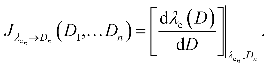 27
27
3 Results and discussion
To illustrate and validate the proposed method, mesoporous SiO2 thin film embedded with CdS SNPs grown inside pores has been chosen as a model example. Mesoporous thin films (MTFs) synthesized via the sol–gel route have been selected due to their excellent optical properties, high degree of reproducibility and, especially, on account of their pore distribution which assures the r < rexc condition,‡ constraining the growth of the SNP to the MTF pore size and spatially fixing them. After analyzing the validity of the approach and its characteristics for this system, the DdD method is extended to other nanocomposites reported in the literature, obtaining the PSD of other SNPs in arbitrary media. Finally, a statistical analysis comparing the spectroscopic and microscopic methods for all studied cases is performed.3.1 Model case: CdS@SiO2 MTF
CdS SNPs were grown inside SiO2 MTF by precipitation, following the SILAR route whose procedure is shown in S1-ESI.† In this synthesis pathway, precursor concentrations, infiltration times or/and number of cycles performed are the variables that rule the CdS SNP growth. Pores of the MTF may host SNPs of different sizes and it is even possible that more than one SNP grows within each pore. Fig. 2 shows UV-Vis absorbance spectra of MTFs resulting from CdjSk@SiO2 SILAR cycles (j,k = 1,…,4). It is interesting to observe that due to the polydispersity of the sample, the resulting spectrum for each cycle does not exhibit a defined exciton peak.24 CdS SNPs inside the MTF pores behave as a dilute system of non-correlated particles; thus the signal is the superposition of the spectra of different size SNPs in the nanocomposite. | ||
| Fig. 2 Absorbance spectra of CdS@SiO2 – AbsCdS(λ) – with different CdS loadings produced by a diverse number of SILAR cycles. | ||
To obtain the PSD of the CdS@SiO2 samples applying the DdD method, the measured extinction spectrum was pre-processed by subtracting the extinction from the substrate and the mesoporous thin film, hence obtaining only the absorbance from the nanoparticles embedded in the pores AbsCdS(λ). Afterwards, to build the matrix system described in eqn (1) and (2), a discretization of the inputs AbsCdS(λ) and AbsDB(λ,λe) had to be fulfilled. A detailed discussion of this process is included in S2.2-ESI.† In particular, for the CdS case under study, the database of ref. 24 was selected to fulfill the Δλe ≈ 0 criteria which ensures an appropriate resolution in the PSD histogram. CdS molar absorption and the empirical function D(λe) data were considered as shown in S2.3-ESI.†
Fig. 3 shows the normalized PSD obtained by the DdD method (blue histograms) in comparison with the PSD obtained by Cs-corrected HRSTEM analysis (red histograms) for different SILAR loadings of CdS NPs (j,k = 1, 2 and 4). It is possible to observe a very good agreement between both methods, exhibiting a more localized distribution for cycle Cd1S1 that spreads out to higher particle sizes when incrementing the SILAR cycles. This behavior with SILAR cycles is expected for the growth of CdS particles inside the (8.0 ± 0.5) nm pores. It can be observed that the DdD method did not only recover the main diameter value, but it was also able to determine a low weight population associated with larger diameters, also observed in HRSTEM images. It is worth noting that the agreement between the two methods is largely due to the consideration of the molar absorption ε(λe) that properly weights the different sizes in the deconvolution process. There is a discrepancy between DdD and Cs-corrected HRSTEM for particles of D < 2.5 nm since the coefficient C (2 nm) derived from the DdD analysis includes all contributions for sizes below this threshold as the database included values from D = 2 nm. Consequently, it is recommended to disregard the coefficient associated with the lowest diameter (see filter option in the Web app section).
 | ||
| Fig. 3 HRSTEM images, their respective histograms (red), and the PSDs determined by DdD (blue) for Cd1S1, Cd2S2 and Cd4S4. Histograms have been computed counting over 100–300 SNPs. | ||
Characteristic Cs-corrected HRSTEM images included in Fig. 3 clearly show the particle size increment in the PSDs. In these images, 2D projections of spherical SNPs were considered. However, in these micrographs, it is not possible to define a unique dimension determination for particle size characterization since they exhibit an oblate feature. During heat treatment of the MTF, where template removal and the network condensation take place simultaneously, a uniaxial contraction of 35% approximately occurs in the axis perpendicular to the substrate.28 This shrinkage generates connected oblate air spheroid pores where the minor axis pore dimension for SiO2 F127 molded thin films is near 3 nm where the major axis pore dimension is around 8 nm. Details on SiO2 MTF structural characterization can be found in S1-ESI.†
Thus, in Fig. 4(a) and (b) oblate particles with minor and major axes, dm and dM respectively were considered for the Cd2S1 SILAR cycle. The axis average values obtained from PSD are different: dm = (3.0 ± 0.5) nm and dM = (3.8 ± 0.8) nm. This indicates a NP growth limited by the pore size that adapts to the pore shape with the characteristic uniaxial contraction when the MTF is calcined.28Fig. 4(c) shows the PSD for  which exhibits a histogram nearly similar to that obtained by DdD (Fig. 4(e)). The average values derived from Fig. 4(c) and (e) are DHRSTEM = (3.0 ± 0.6) nm and DDdD = (3.0 ± 0.4) nm respectively. Thus, this method is able to obtain from the UV-Vis spectra an effective particle size insensitive to the SNP geometrical shape.
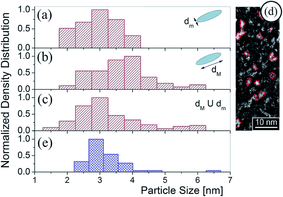 | ||
Fig. 4 Histograms from the fitting ellipses for the HRSTEM corresponding to the (a) dm, minor diameter, (b) dM, major diameter, (c) diameter  and (d) an example of the HRTEM micrograph for the Cd2S1 cycle. (e) The PSD obtained with the DdD method. and (d) an example of the HRTEM micrograph for the Cd2S1 cycle. (e) The PSD obtained with the DdD method. | ||
It is also interesting to note from Cs-corrected HRSTEM images in Fig. 3 and 4 that as SILAR cycles proceed, CdS NPs start to connect between pores reaching very high SNP connectivity for CdjSk cycles with j,k ≥ 4. Despite this connection, DdD has been able to recover reliable average diameters.
Fig. 5 compiles the mean particle size for the DdD method and from the Cs-corrected HRSTEM images in a quantitative way demonstrating the agreement between results obtained with both spectroscopic and microscopic experiments. Mean particle sizes were obtained using the mean value μ of the LogNormal distribution given in S3-ESI.† In Fig. 5 two extra SILAR cycle steps, Cd3S2 and Cd3S3 have been analyzed by the DdD method (absorbance spectra included in Fig. 2, no microscope associated images available).
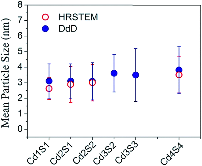 | ||
| Fig. 5 Mean Particle Size comparison for different SILAR cycles obtained by a LogNormal fit of Cs-corrected HRSTEM (empty red dots) and by the DdD method done over the absorbance spectra of Fig. 2 (solid blue dots). | ||
3.2 Method validation for SNPs embedded in arbitrary matrices
In order to prove the versatility of the DdD method, it was applied to other systems taken from literature data: CdS and other SNPs, such as CdSe, included in diverse media (liquid, soft or solid). Fig. 6 shows the comparison between the DdD results and the transmission microscopy images for four systems using the LogNormal distribution fitting already employed in Fig. 5.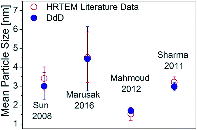 | ||
| Fig. 6 Mean Particle Size of LogNormal distribution fitting of the PSD obtained with TEM or HRTEM images (empty red dots) and the corresponding DdD analysis (solid blue dots) from some literature examples. | ||
Marusak et al.30 synthesized intra and extra-cellular CdS SNPs produced by Escherichia coli through metabolic cysteine. In this bio-synthesized CdS SNP system, the DdD method again shows a good agreement between the obtained mean size values and the corresponding values obtained from microscopy, even without subtracting the light scattering contribution by bacteria and macromolecules. The larger standard deviation resulting from the DdD method is probably a consequence of this baseline from light scattering.
CdSe synthesized by Mahmoud et al.31 in aqueous solution at 65 °C using 2-mercaptoethanol as a capping agent exhibits nearly monodisperse 3 nm CdSe SNPs, as determined both by DdD and TEM (Fig. 6). CdSe SNPs grown on ITO substrates using a wet chemical synthesis by Sharma et al.10 also show a very good agreement between TEM and the DdD method, giving a mean diameter of 1.7 nm and also a very monodisperse population. It is worth mentioning that although the two CdSe samples showed significantly different mean diameters, each one matched TEM and DdD data with the same database. Thus, with a database built considering an appropriate sampling distance and a wide range of sizes (S.2.2-ESI†) the average particle size and PSD can easily be obtained with the DdD method even for particles in different environments.
3.3 Statistical analysis
In Sections 3.1 and 3.2, SNPs embedded in diverse media were studied comparing transmission microscopy images (TEM, HRTEM or HRSTEM) and DdD methods. To analyze the confidence in the comparisons, a paired t-test was performed to compare if differences were significant. Table 1 shows the mean values for cycle Cd2S1 of Fig. 5 and for all cases of Fig. 6 as examples of different systems. To compare the mean values obtained by DdD methods, the tcalc parameter was calculated as indicated in eqn (3) | (3) |
 is the absolute value of the mean difference.
 ![[x with combining macron]](https://www.rsc.org/images/entities/i_char_0078_0304.gif) DdD = ln(xDdDc) and TEM = ln(xTEMc) are the mean values of the normal distribution associated with the LogNormal distribution of centers xDdDc and xTEMc for DdD and transmission microscopy methods respectively (see Section S.3† for more details). In eqn (3), s corresponds to the standard deviation of the differences and n the number of degrees of freedom.
DdD = ln(xDdDc) and TEM = ln(xTEMc) are the mean values of the normal distribution associated with the LogNormal distribution of centers xDdDc and xTEMc for DdD and transmission microscopy methods respectively (see Section S.3† for more details). In eqn (3), s corresponds to the standard deviation of the differences and n the number of degrees of freedom.
| Sample | x DdDc (nm) | x TEMc (nm) |
DdD − TEM (nm) |
|---|---|---|---|
| SILAR Cd2S1 | 3.00 | 2.96 | 0.13 |
| Sharma 2011 | 1.70 | 1.49 | −0.15 |
| Mahmoud 2012 | 2.97 | 3.20 | 0.13 |
| Sun 2008 | 2.91 | 3.35 | −0.07 |
| Marusak 2016 | 4.15 | 4.34 | −0.05 |
| Absolute mean difference (d) | 0.02 | ||
| Standard deviation (s) | 0.11 | ||
From the information obtained in Table 1, tcalc = 1.04 was obtained, which is smaller than ttable = 2.776 for 95% confidence and 4 degrees of freedom (n = 4, α = 0.05). The obtained value for tcalc indicates that the confidence could be restricted up to 70% which ensures that the results obtained by DdD and the analysis performed over the transmission microscopy images are statistically equal, proving robustness of the proposed method.
4 Web app
To ease the implementation of the DdD method, a free web app32 was developed for the community to analyze their own systems. This web application was coded using Python and the library Plotly.33 Fig. S6† shows the app interface before using and after applying DdD an absorbance spectrum. The app requires the absorbance sample spectrum, the database absorbance spectra and the Jacobian. Files can be loaded as CSV or XLS. When the data is loaded to the app, the DdD method can be applied deconvoluting the absorbance sample spectrum and showing the PSD. A filter option is also available; this feature applies a threshold value to disregard all contributions for sizes below the defined threshold. This option is useful to avoid accumulative errors in the lowest coefficient. In addition, the distribution is fitted with a LogNormal function that returns the mean and standard deviation parameters.5 Conclusions
In summary, we have demonstrated that the numerical deconvolution of a measured absorbance spectrum using an absorption spectrum database gives the PSD of SNPs dispersed in arbitrary media. In particular, absorption spectra of CdS NPs embedded in mesoporous silica thin films have been analyzed by DdD method. The obtained PSD reproduces with a deviation of less than 5% that obtained with Cs-corrected HRSTEM images, even considering the deviation from sphericity of real SNPs. The validation of the DdD method extended to other SNPs and matrices allowed us to conclude that DdD is a successful resource to analyze SNP sizes and obtain their PSD regardless of the media where they are included. For widespread application of the DdD method, we have developed a web app for the community to obtain the PSD of their own SNPs.In comparison with previously reported methods, the DdD approach only uses UV-Vis spectra, which is a ubiquitous, non-invasive technique that makes it possible to use DdD as an automated routine. It also takes into consideration the complete spectral information which is identified by the exciton position λe, which in conjunction with the application of a Jacobian λe → D transformation, returns a well-weighted and defined PSD. We have proved that it is applicable for a wide range of cases ranging from solid to soft media, including colloids and even inside cells and covering diverse SNPs. Thus, with an appropriate database, the method is applicable to other materials as other chalcogenides, InP, GaAs or perovskites. The possibility to use a simple and practical technique to get the SNP PSD in complex systems, eases the development of composed nanostructures, being able to monitor online processes, such as the growth of SNPs during a high temperature reaction or the formation inside solar cells which turns DdD into a high-throughput strategy.
Conflicts of interest
There are no conflicts to declare.Acknowledgements
This work was supported by Universidad de Buenos Aires (UBACyT 20020170200298B) and RECOLA (ELAC2015/T02-0830). D. O., S. A. B. and M. L. M. R are members of CONICET. The Spanish Ministry of Economy and Competitiveness (Grant No. MAT2017-82970-C2, including FEDER) and the Aragon regional government (E26), Spain. The microscopy studies were conducted in the LMA at INA, Universidad de Zaragoza. AM acknowledges the National Natural Science Foundation of China for the projects NFSC-21850410448 and NSFC-21835002.References
- M. V. Kovalenko, L. Manna, A. Cabot, Z. Hens, D. V. Talapin, C. R. Kagan, V. I. Klimov, A. L. Rogach, P. Reiss and D. J. Milliron, ACS Nano, 2015, 9(2), 1012–1057 CrossRef CAS PubMed.
- E. H. Sargent, Nat. Photonics, 2012, 6, 133 CrossRef CAS.
- F. Purcell-Milton and Y. K. Gun'ko, J. Mater. Chem., 2012, 22, 16687–16697 RSC.
- N. Matsumura, H. Endo and J. Saraie, Phys. Status Solidi B, 2002, 229, 1039–1042 CrossRef CAS.
- M. Frasco and N. Chaniotakis, Sensors, 2009, 9, 7266–7286 CrossRef CAS.
- D. W. Bahnemann, C. Kormann and M. R. Hoffmann, J. Phys. Chem., 1987, 91, 3789–3798 CrossRef CAS.
- C. Murray, D. J. Norris and M. G. Bawendi, J. Am. Chem. Soc., 1993, 115, 8706–8715 CrossRef CAS.
- C. A. Leatherdale, W.-K. Woo, F. V. Mikulec and M. G. Bawendi, J. Phys. Chem. B, 2002, 106, 7619–7622 CrossRef CAS.
- I. Moreels, K. Lambert, D. Smeets, D. De Muynck, T. Nollet, J. C. Martins, F. Vanhaecke, A. Vantomme, C. Delerue and G. Allan, ACS Nano, 2009, 3, 3023–3030 CrossRef CAS PubMed.
- M. Sharma, A. Sharma, N. Mishra and R. Pandey, Mater. Res. Bull., 2011, 46, 453–459 CrossRef CAS.
- A. Fischereder, M. L. Martinez-Ricci, A. Wolosiuk, W. Haas, F. Hofer, G. Trimmel and G. J. Soler-Illia, Chem. Mater., 2012, 24, 1837–1845 CrossRef CAS.
- L. B. Scaffardi, N. Pellegri, O. De Sanctis and J. O. Tocho, Nanotechnology, 2004, 16, 158 CrossRef.
- W. Haiss, N. T. Thanh, J. Aveyard and D. G. Fernig, Anal. Chem., 2007, 79, 4215–4221 CrossRef CAS PubMed.
- J. Santillán, L. Scaffardi and D. Schinca, J. Phys. D: Appl. Phys., 2011, 44, 105104 CrossRef.
- V. M. Sánchez, E. D. Martínez, M. L. Martínez Ricci, H. Troiani and G. Soler-Illia, J. Phys. Chem. C, 2013, 117, 7246–7259 CrossRef.
- L. E. Brus, J. Chem. Phys., 1984, 80, 4403–4409 CrossRef CAS.
- S. Lee, L. Jönsson, J. W. Wilkins, G. W. Bryant and G. Klimeck, Phys. Rev. B, 2001, 63, 195318 CrossRef.
- Y. Wang and N. Herron, J. Phys. Chem., 1991, 95, 525–532 CrossRef CAS.
- N. S. Pesika, K. J. Stebe and P. C. Searson, J. Phys. Chem. B, 2003, 107, 10412–10415 CrossRef CAS.
- O. I. Micic, C. J. Curtis, K. M. Jones, J. R. Sprague and A. J. Nozik, J. Phys. Chem., 1994, 98, 4966–4969 CrossRef CAS.
- D. Segets, KONA Powder Part. J., 2016, 2016012 Search PubMed.
- D. Segets, J. Gradl, R. K. Taylor, V. Vassilev and W. Peukert, ACS Nano, 2009, 3, 1703–1710 CrossRef CAS PubMed.
- D. Segets, J. M. Lucas, R. N. Klupp Taylor, M. Scheele, H. Zheng, A. P. Alivisatos and W. Peukert, ACS Nano, 2012, 6, 9021–9032 CrossRef CAS.
- J. Thessing, J. Qian, H. Chen, N. Pradhan and X. Peng, J. Am. Chem. Soc., 2007, 129, 2736–2737 CrossRef CAS PubMed.
- R. D. Harris, S. Bettis Homan, M. Kodaimati, C. He, A. B. Nepomnyashchii, N. K. Swenson, S. Lian, R. Calzada and E. A. Weiss, Chem. Rev., 2016, 116, 12865–12919 CrossRef CAS PubMed.
- W. W. Yu, L. Qu, W. Guo and X. Peng, Chem. Mater., 2003, 15, 2854–2860 CrossRef CAS.
- J. Mooney and P. Kambhampati, J. Phys. Chem. Lett., 2013, 4(19), 3316–3318 CrossRef CAS.
- G. Soler-Illia, P. Angelomé, M. Fuertes, A. Calvo, A. Wolosiuk, A. Zelcer, M. Bellino and E. Martínez, J. Sol-Gel Sci. Technol., 2011, 57, 299–312 CrossRef CAS.
- Z.-B. Sun, X.-Z. Dong, W.-Q. Chen, S. Shoji, X.-M. Duan and S. Kawata, Nanotechnology, 2007, 19, 035611 CrossRef PubMed.
- K. Marusak, Y. Feng, C. Eben, S. Payne, Y. Cao, L. You and S. Zauscher, RSC Adv., 2016, 6, 76158–76166 RSC.
- W. E. Mahmoud, A. M. Al-Amri and S. Yaghmour, Opt. Mater., 2012, 34, 1082–1086 CrossRef CAS.
- https://determinenpssizes.herokuapp.com/ .
- Plotly Technologies Inc., Collaborative data science, Montréal, QC, 2015. https://plot.ly, accessed February 2019 Search PubMed.
Footnotes |
| † Electronic supplementary information (ESI) available. See DOI: 10.1039/c9na00344d |
| ‡ Where rexc = εrrme/μ, μ is the exciton effective mass, me is the electron mass, εr is the material dielectric constant and rB is the Bohr radius (e.g. rCdSeexc = 5.4 nm; rCdSexc = 5.8 nm). |
| This journal is © The Royal Society of Chemistry 2019 |